

TriQuint Semiconductor Inc TQ3131 Datasheet
WIRELESS COMMUNICATIONS DIVISION
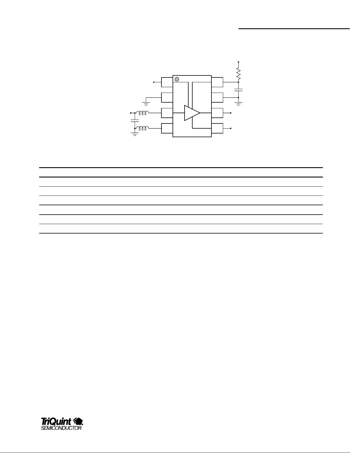
Control
Logic
C2
C2
L1
VDD
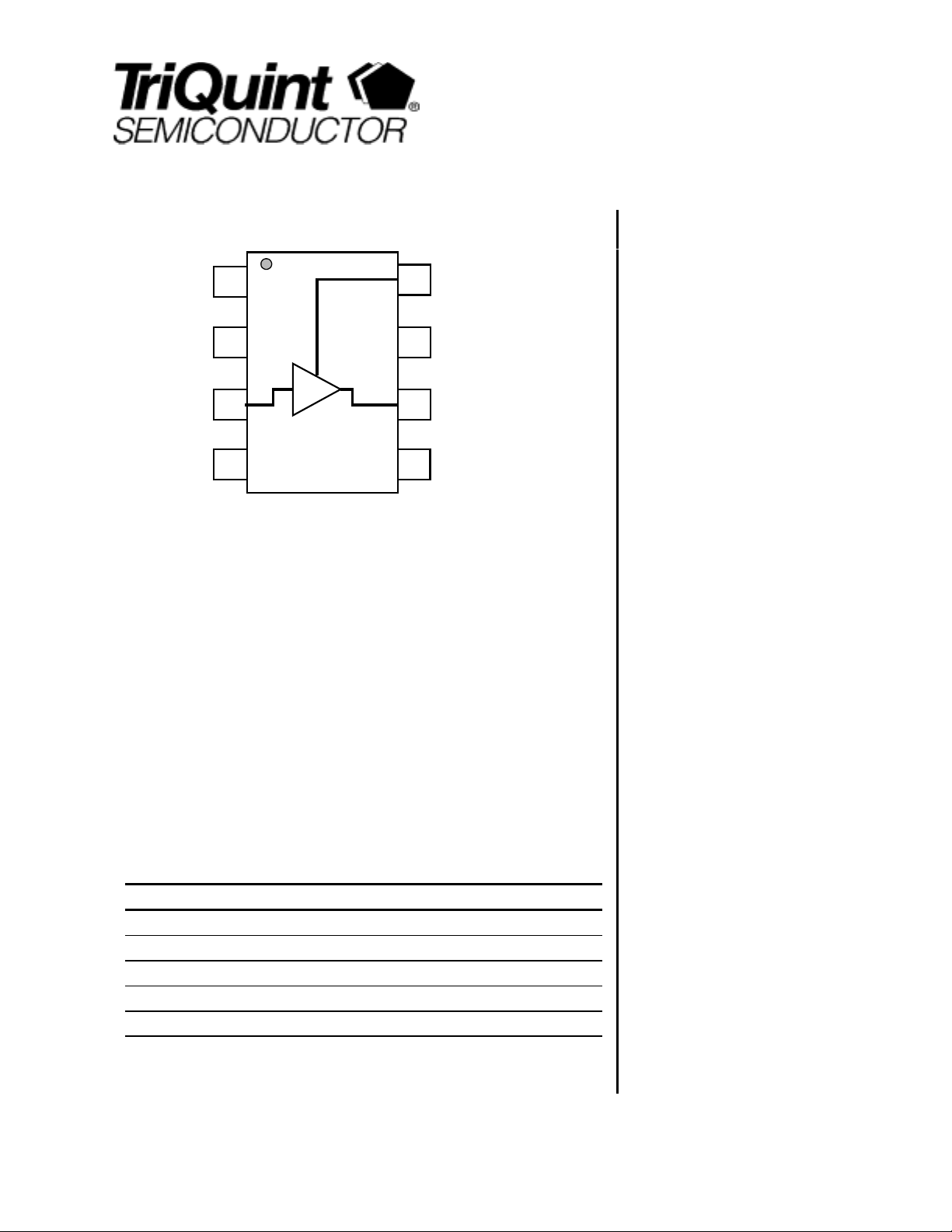
TQ3131
DATA SHEET
GND
RF
IN
GND
GND
RF
OUT
C3
50 ohm
RF Out
Control
Logic
Product Description
The TQ3131 is a 3V, RF LNA IC designed specifically for Cellular band CDMA/AMPS
applications. It’s RF performance meets the requirements of products designed to
the IS-95 and AMPS standards. The TQ3131 is designed to be used with the
TQ5131 (CDMA/AMPS mixer) which provides a complete CDMA receiver for
800MHz dual-mode phones.
The LNA incorporates on-chip switches which determine CDMA, AMPS, and bypass
mode select. When used with the TQ5131 (CDMA RFA/mixer), four gain states are
available. The RF output port is internally matched to 50
design and keeping the number of external components to a minimum. The TQ3131
achieves good RF performance with low current consumption, supporting long
standby times in portable applications. Coupled with the very small SOT23-8
package, the part is ideally suited for Cellular band mobile phones.
Electrical Specifications
Parameter Min Typ Max Units
Frequency 832 894 MHz
Gain 13.0 dB
Noise Figure 1.4 dB
Input 3rd Order Intercept 10.0 dBm
DC supply Current 10.5 mA
Note 1: Test Conditions: Vdd=2.8V , Tc=25C, RF fr equency=88 1MHz, CDMA High Gain state.
1
Ω
, greatly simplifying the
3V Cellular Band
CDMA/AMPS LNA IC
Features
Small size: SOT23-8
Single 3V operation
Low-current operation
Gain Select
Mode Select
High IP3 performance
Few external components
Applications
IS-95 CDMA Mobile Phones
AMPS Mobile Phones
Dual Mode CDMA Cellular applications
832-870MHz CDMA applications
For additional information and latest specifications, see our website: www.triquint.com 1
TQ3131
Data Sheet
Electrical Characteristics
Parameter Conditions Min. Typ/Nom Max. Units
RF Frequency 832 881 894 MHz
CDMA Mode-High Gain
Gain 11.5 13.0 dB
Noise Figure 1.4 2.0 dB
Input IP3 8.0 10.0 dBm
LNA IN Return Loss (with external matching) 10 dB
LNA OUT Return Loss 10 dB
Supply Current 10.5 13.5 mA
Bypass Mode
Gain -3.0 -2.0 dB
Noise Figure 2.0 3.0 dB
Input IP3 18.0 30.0 dBm
LNA IN Return Loss (with external matching) 10 dB
LNA OUT Return Loss 10 dB
Supply Current 1.2 2.5 mA
AMPS Mode
Gain 8.5 11.0 dB
Noise Figure 1.6 2.2 dB
Input IP3 2.0 3.0 dBm
LNA IN Return Loss (with external matching) 10 dB
LNA OUT Return Loss 10 dB
Supply Current 4.0 5.5 mA
Supply Voltage 2.7 2.8 3.3 V
Note 1: Test Conditi ons: Vdd=2.8V, RF=881MHz, TC = 25° C, unless ot herwise specified.
Note 2: Min/Max limits are at +25
°
C case temperature, unless otherwise specified.
Absolute Maximum Ratings
Parameter Value Units
DC Power Supply 5.0 V
Power Dissipation 500 mW
Operating Temperature -40 to 85 C
Storage Temperature -60 to 150 C
Signal level on inputs/outputs +20 dBm
Voltage to any non supply pin +0.3 V
2 For additional information and latest specifications, see our website: www.triquint.com
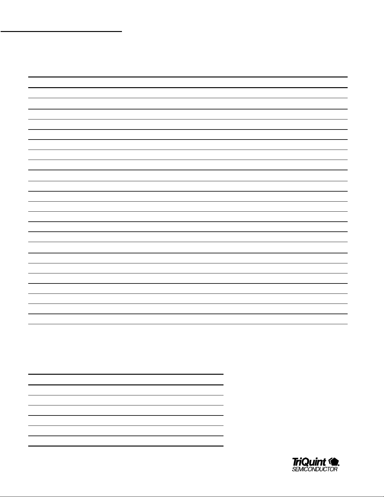
Typical Performance
Test Conditions, unless Otherwise Spec ified: Vdd=2.8V, Tc=+25C, RF=881MHz
CDMA High Gain Mode
Gain v Freq v Temp
15.0
14.5
14.0
13.5
13.0
12.5
12.0
Gain (dB)
11.5
11.0
10.5
10.0
850 860 870 880 890 900 910
Frequency (MHz)
-30C
+25C
+85C
TQ3131
Data Sheet
CDMA High Gain Mode
Idd v Vdd v Temp
13.50
13.00
12.50
12.00
11.50
11.00
Idd (mA)
10.50
10.00
9.50
9.00
2.5 2.7 2.9 3.1 3.3
Vdd (V)
-30C
+25C
+85C
CDMA High Gain Mode
IIP3 v Freq v Temp
13.5
13.0
12.5
12.0
IIP3 (dBm)
11.5
11.0
850 860 870 880 890 900 910
Frequency (MHz)
CDMA High Gain Mode
Noise Figure v Freq v Temp
1.90
1.70
1.50
1.30
1.10
Noise Figure (dB)
0.90
0.70
0.50
850 860 870 880 890 900 910
Frequency (MHz)
-30C
+25C
+85C
-30C
+25C
+85C
AMPS Mode
Gain v Freq v Temp
13.0
12.5
12.0
11.5
11.0
Gain (dB)
10.5
10.0
9.5
-30C
+25C
+85C
9.0
850 860 870 880 890 900 910
Frequency (MHz)
AMPS Mode
IIP3 v Freq v Temp
7.0
6.5
6.0
5.5
5.0
IIP3 (dBm)
4.5
4.0
3.5
3.0
850 860 870 880 890 900 910
Frequency (MHz)
-30C
+25C
+85C
For additional information and latest specifications, see our website: www.triquint.com 3
TQ3131
Data Sheet
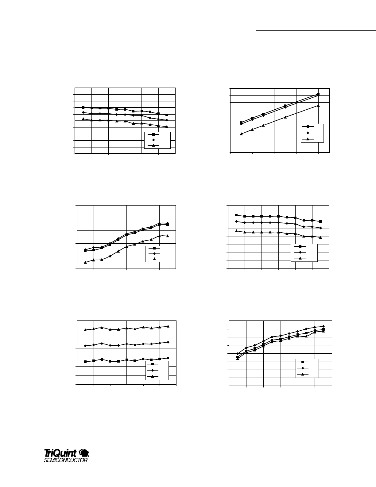
AMPS Mode
Noise Figure v Freq v Temp
2.50
2.00
1.50
1.00
Noise Figure (dB)
0.50
0.00
850 860 870 880 890 900 910
Frequency (MHz)
AMPS Mode
Idd v Vdd v Temp
5.50
5.00
4.50
Idd (mA)
4.00
3.50
3.00
2.5 2.7 2.9 3.1 3.3
Vdd (V)
-30C
+25C
+85C
-30C
+25C
+85C
BYPASS Mode
Gain v Freq v Temp
-1.0
-1.2
-1.4
-1.6
-1.8
-2.0
-2.2
Gain (dB)
-2.4
-2.6
-2.8
-3.0
850 860 870 880 890 900 910
Frequency (MHz)
BYPASS Mode
Noise Figure v Freq v Temp
2.50
2.00
1.50
1.00
Noise Figure (dB)
0.50
0.00
850 860 870 880 890 900 910
Frequency (MHz)
-30C
+25C
+85C
-30C
+25C
+85C
BYPASS Mode
IIP3 v Freq v Temp
35.0
34.0
33.0
32.0
31.0
30.0
IIP3 (dBm)
29.0
28.0
27.0
850 860 870 880 890 900 910
Frequency (MHz)
-30C
+25C
+85C
BYPASS Mode
Idd v Vdd v Temp
1.80
1.60
1.40
1.20
1.00
0.80
Idd (mA)
0.60
0.40
0.20
0.00
2.5 2.7 2.9 3.1 3.3
Vdd (V)
-30C
+25C
+85C
4 For additional information and latest specifications, see our website: www.triquint.com
Application/Test Circuit
TQ3131
Data Sheet
Vdd
Control
Logic
C2
Vdd
C2
R1
GND
(paddle)
LNA input LNA output
L1
RF in
GND
RF
out
C1
Lbrd
LNA
GND
C3
Control Logic
Bill of Material for TQ3131 LNA Application/Test Circuit
Component Reference Designator Part Number Value Size Manufacturer
Receiver IC U1 TQ3131 SOT23-8 TriQuint Semiconductor
Capacitor C1 3.3pFd 0402
Capacitor C2 8.2pF 0402
Resistor R1
3.3Ω
Inductor L1 15nH 0402
Inductor Lbrd See application note
0402
For additional information and latest specifications, see our website: www.triquint.com 5
 Loading...