

TriQuint Semiconductor Inc TQ2061MC Datasheet
T R I Q U I N T S E M I C O N D U C T O R , I N C .
1
SYSTEM TIMING
PRODUCTS
For additional information and latest specifications, see our website: www.triquint.com
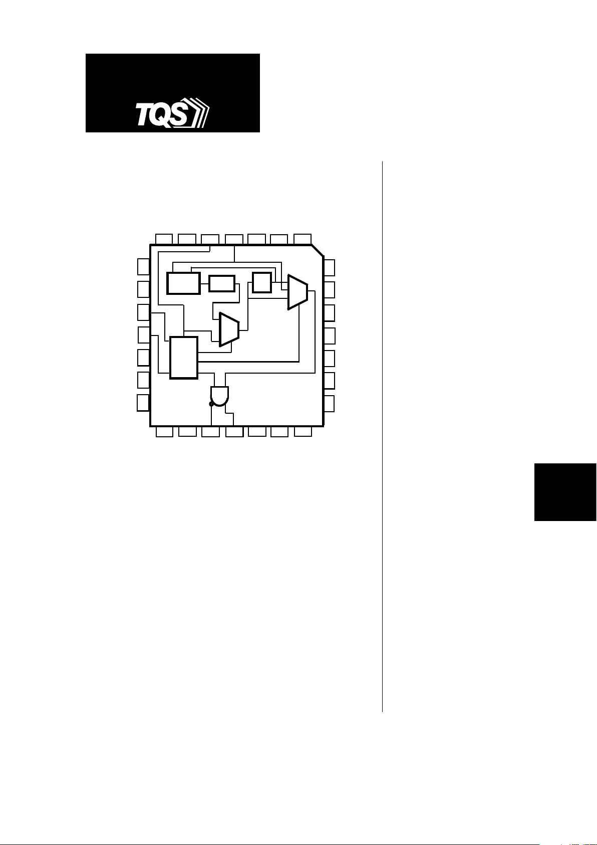
Figure 1. Pinout Diagram
TriQuint’s TQ2061 is a high-frequency clock generator. It utilizes a 25 MHz
to 35 MHz TTL input to generate a 500 MHz to 700 MHz PECL output. The
TQ2061 has a completely self-contained Phase-Locked Loop (PLL) running
at 500 MHz to 700 MHz. This stable PLL allows for a low period-to-period
output jitter of 70 ps (max), and enables tight duty cycle control of 55% to
45% (worst case).
The TQ2061 provides optional 200-ohm on-chip pull-down resistors which
are useful if the output is AC-coupled to the device being driven. In order
to use these resistors, pin 20 (PDR2) should be connected to pin 21 (QN),
and pin 23 (PDR1) should be connected to pin 22 (Q).
Various test modes on the chip simplify debug and testing of systems by
slowing the clock output or by bypassing the PLL.
TQ2061
High-Frequency
Clock Generator
Features
•
Output frequency range:
500 MHz to 700 MHz
•
One differential PECL output:
600 mV (min) swing
•
Common-mode voltage:
V
DD
–1.2 V (max),
V
DD
–1.6 V (min)
•
Period-to-period output jitter:
25 ps peak-to-peak (typ)
70 ps peak-to-peak (max)
•
Reference clock input:
25 MHz to 35 MHz TTL-level
crystal oscillator
•
Self-contained loop filter
•
Optional 200 Ω pull-down
resistors for AC-coupled outputs
•
+5 V power supply
•
28-pin J-lead surface-mount
package
•
Ideal for designs based on DEC
Alpha AXP
™
processors
1
4
3
2
NC
NC
NC
NC
NC
NC
AGND
GND
PDR1
Q
QN
PDR2
EVDD
VDD
NC
GND
NC
NC
TEST1
28
27
26
19
20
21 22
23
24
25
11
10
9 8
7
6
5
16
17
18
13
12
15
14
NC
NC
GND
REFCLK
TESTIN
NC
GND
Control
Phase
VCO
MUX
MUX
÷20
TEST2
TQ2061
2
For additional information and latest specifications, see our website: www.triquint.com
Mode TEST1 TEST2 TESTIN
1
REFCLK Q, QN
1 (Test) 0 0 “don’t care” f
REFCLK
f
REFCLK
2
2 (Test) 0 1 “don’t care” “don't care” 0, 1
3 (Test) 1 0 f
TESTCLK
“don't care” f
TESTCLK
4 (Bypass) 1 1 0 f
REFCLK
f
REFCLK
5 (Normal) 1 1 1 f
REFCLK
20 x f
REFCLK
3
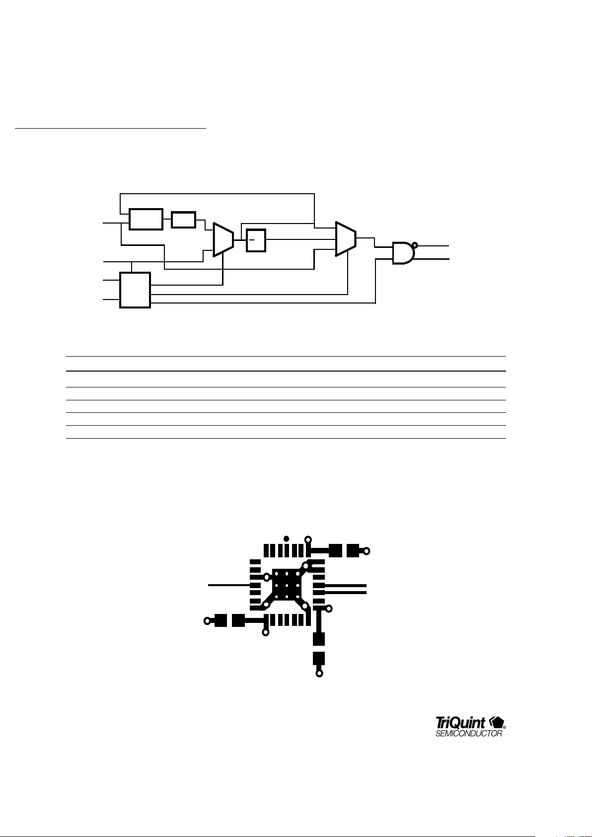
Figure 2. Simplified Block Diagram
Table 1. Mode Selection
Notes: 1. In mode 3, TESTIN may be used to bypass the PLL.
2. REFCLK = 25 MHz to 35 MHz.
3. Q, QN = 500 MHz to 700 MHz.
Pin 1
Q
QN
REFCLK
(
from TTLoscillator
)
GND
VDD
VDD
VDD
GND
GND
GND
0.1 µF
0.1 µF
0.1 µF
50 OHMS
Figure 3. Recommended Layout
(Not to scale)
(From TTL Oscillator)
(25MHz to
35 MHz)
Phase
REFCLK
TESTIN
TEST1
TEST2
Q
QN
MUX
VCO
MUX
: 20
(500 MHz
to
700 MHz)
Control
 Loading...