

TriQuint Semiconductor Inc TGF4230-EEU Datasheet
T R I Q U I N T S E M I C O N D U C T O R , I N C .
TGF4230-EEU Discr
1200 µm X 0.5 µm HFET
●
Nominal Pout of 28.5-dBm at 8.5-GHz
●
Nominal Gain of 10.0- dB at 8.5-GHz
●
Nominal PAE of 55% at 8.5 - GHz
●
Suitable for High-Reliability Applications
●
0,572 x 0,699 x 0,102 mm (0.023 x 0.028 x 0.004 in.)
●
PHOTO ENLARGEMENT
1.2mm ete HFET
4230
DESCRIPTION
TriQuint Semiconductor, Inc. • Texas Facilities • (972) 995-8465
The Triquint TGF4230 -EEU is a single gate 1.2 mm Discrete GaAs Heterostructure Field
Ef fect Transistor (HFET) designed for high- efficiency power applications up to 1 2- GHz in Class A and
Class AB operation.
Bond - pad and backside metalization is gold plated for compatibility with eutectic alloy attach methods
as well as thermocompression and thermosonic wire- bonding processes. The TGF4230-EEU is
readily assembled using automatic equipment.
• www.triquint.com
TGF4230-EEU
EXAMPLE OF
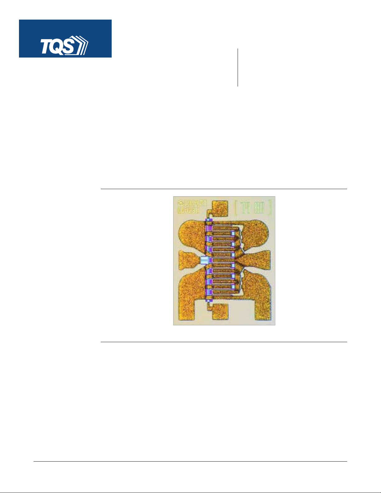
DC I-V CURVES
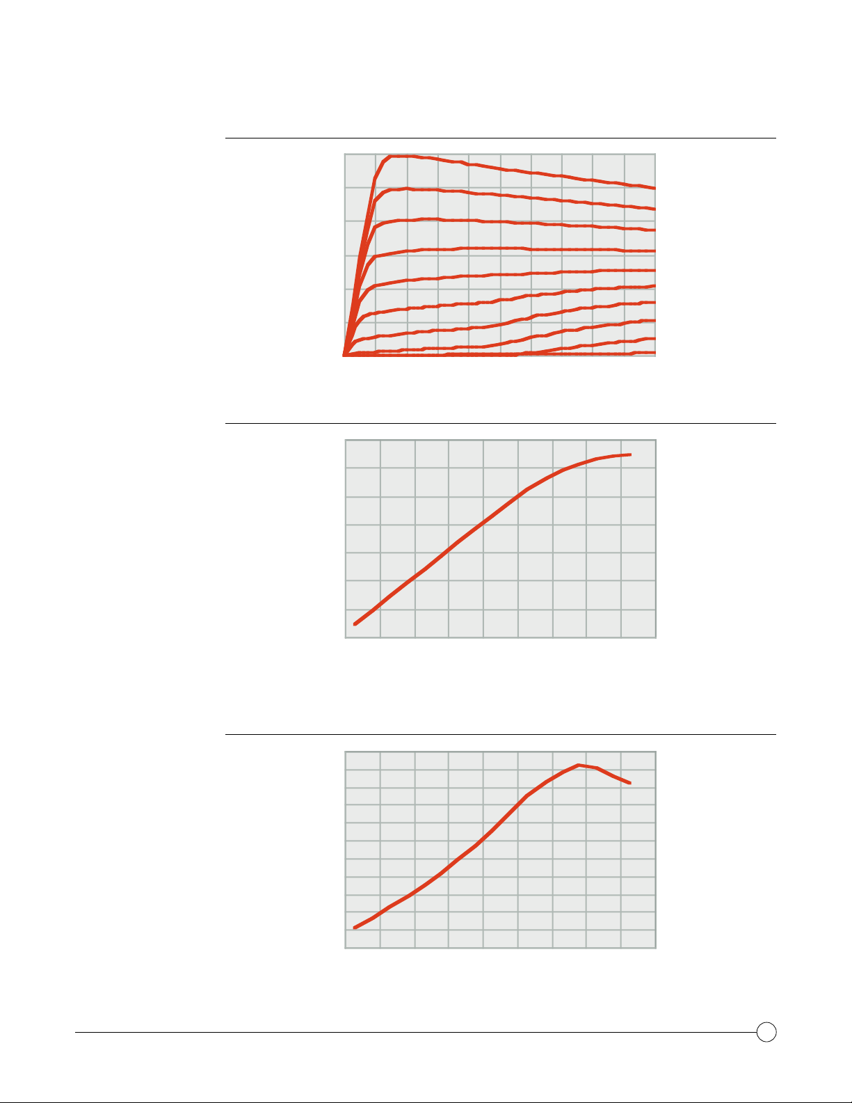
OUTPUT POWER VS.
INPUT POWER
0.3
0.25
0.2
0.15
0.1
Drain Current (A)
0.05
0
012345678910
Drain Voltage (V)
30
28
26
24
22
VG= 0.0 to -2.25 V
(0.25 V steps)
= 25°C
T
A
F = 8.5GHz
VD=8.0V
=50mA*
I
Q
=25°C
T
A
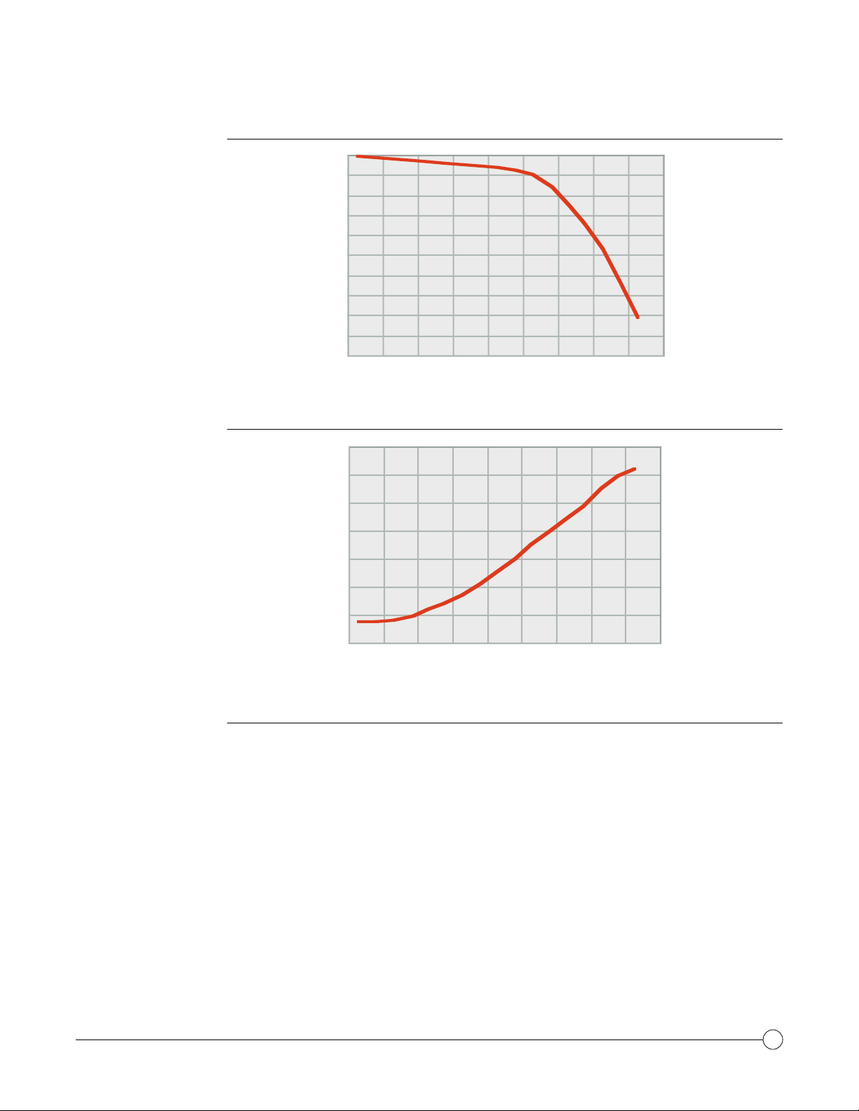
POWER ADDED
EFFICIENCY VS.
INPUT POWER
20
Output Power (dBm)
18
16
4 6 8 10 12 14 16 18 20 22
Input Power (dBm)
Note: IQ is defined as the drain current before application of RF signal at the input.
60
55
50
45
40
35
30
PAE (%)
25
20
15
10
5
4 6 8 10 12 14 16 18 20 22
Input Power (dBm)
F = 8.5GHz
VD=8.0V
=50mA*
I
Q
=25°C
T
A
TriQuint Semiconductor, Inc. • Texas Facilities • (972) 995-8465
• www.triquint.com
2
TGF4230-EEU
GAIN VS.
INPUT POWER
DRAIN CURRENT
VS. INPUT POWER
12
11
10
Gain (dB)
9
8
7
4 6 8 10 12 14 16 18 20 22
Input Power (dBm)
180
160
140
120
100
F =8.5GHz
VD=8.0V
=50mA*
I
Q
=25°C
T
A
F =8.5GHz
VD=8.0V
=50mA*
I
Q
=25°C
T
A
ABSOLUTE
MAXIMUM RATINGS
80
Drain Current (mA)
60
40
4 6 8 10121416182022
Input Power (dBm)
Drain - to- source V oltage, V
. ................................................................................................................ 12 V
DS
Gate - to- source V oltage, VGS......................................................................................................-5 V to 0 V
Mounting temperature (30 sec), T
Storage temperature range, T
.................................................................................................. 320 C
M
............................................................ ................................-65 to 200 C
STG
Power dissipation, PD.................................................................................. (see thermal data on next page)
Operating channel temperature, TCH.............................................................. (see thermal data on next page)
Ratings over base-plate temperature range TBP(unless otherwise noted)
Stresses beyond those listed under “Absolute Maximum Ratings” may cause permanent damage to the device.
These are stress ratings only, and functional operation of the device at these or any other conditions beyond
those indicated “RF and DC Characteristics” is not implied. Exposure to absolute maximum rated conditions for
extended periods of time may affect device reliability.
TriQuint Semiconductor, Inc. • Texas Facilities • (972) 995-8465
• www.triquint.com
3
 Loading...