

TriQuint Semiconductor Inc TGC1411-EPU Datasheet
Advance Product Information
0.3 - 10 GHz Downconverter TGC1411-EPU
Key Features and Performance
• 0.25um pHEMT Technology
• 0.3-10 GHz RF/LO Frequency Range
• 0.15-2.5 GHz IF Frequency Range
• Nominal Conversion Gain of 12 dB
• Bias 3-5V @ 26 mA
• Chip Dimensions 1.8 mm x 2.6mm
Primary Applications
• Satellite Systems
The TriQuint TGC1411-EPU is a double balanced
MMIC mixer design using TriQuint’s proven 0.25 um
Power pHEMT process to support a variety of
communication system applications including satellite.
The double balanced design consists of an integrated
Gilbert cell mixer core, RF/LO baluns, differential
combiner, and output driver amplifier. The TGC1411
may be operated from a single +3 V to +5 V power
supply with typical current draw of 26 mA. The
nominal LO power requirement is -5 dBm. The
TGC1411 may also be operated as an up-converter.
The TGC1411 requires a minimum of off-chip
components employing only a 100 pF off-chip bypass
capacitor for the power supply line. No additional offchip RF matching components are required. Each
device is 100% DC and RF tested on-wafer to ensure
performance compliance. The device is available in
chip form.
RF
IN
IF
OUT
LO
IN
Note: Devices designated as EPU are typically early in their characterization process prior to finalizing all electrical and process
specifications. Specifications are subject to change without notice.
• Point-to-Point Radio
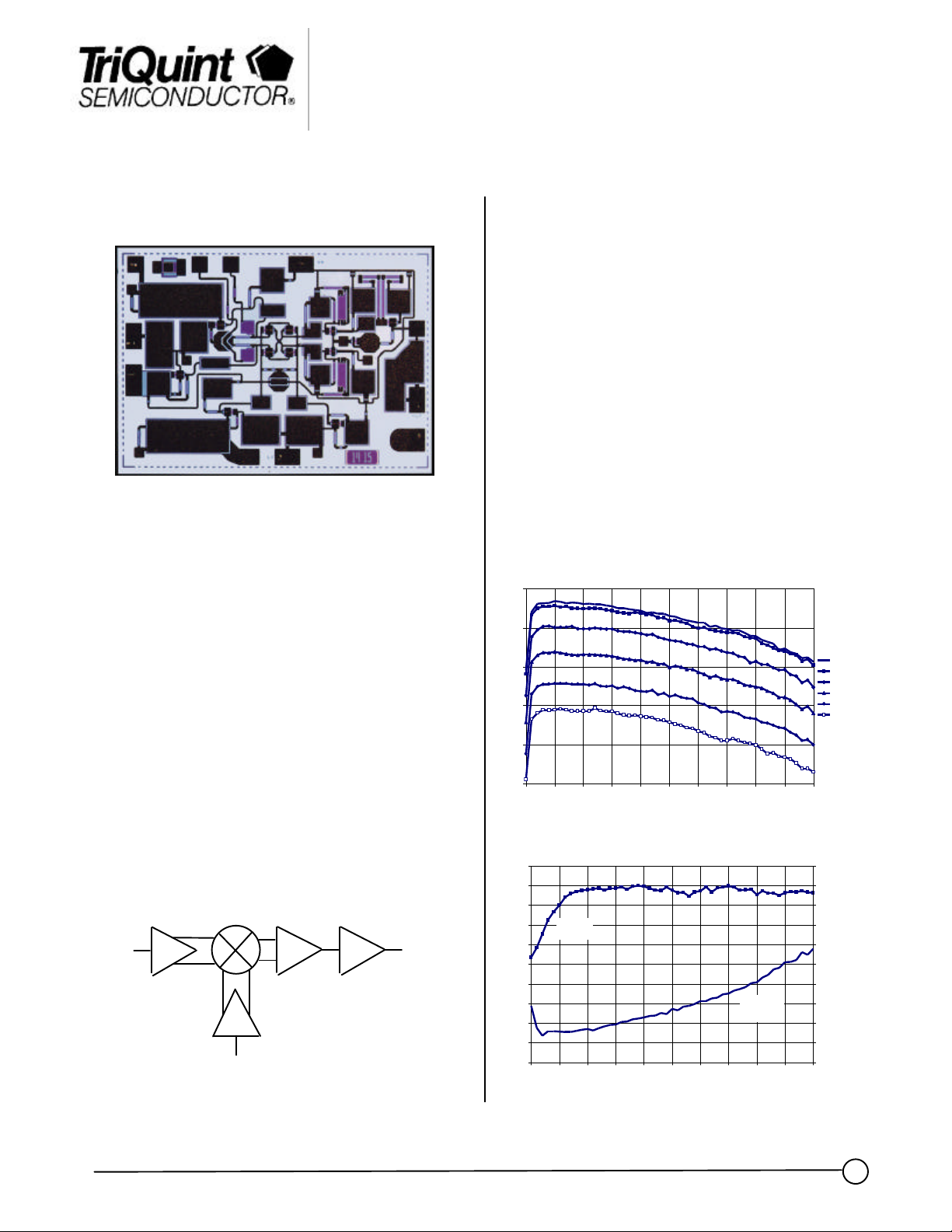
TGA1411 Typical Down-Conversion Gain
TGC 1411
18
15
12
9
Conversion Gain (dB)
6
3
0.1 1.1 2.1 3.1 4.1 5.1 6.1 7.1 8.1 9.1 10.1
TGA1411 Typical P1dB and SSB Noise Figure
TGC 1411
1
0
-1
-2
-3
-4
-5
-6
Output P1dB (dBm)
-7
-8
-9
0.1 1.1 2.1 3.1 4.1 5.1 6.1 7.1 8.1 9.1 10.1
LSB, +5.0V, LO = -5dBm, +25C
RF Frequency (GHz)
LSB, +5.0V, LO = -5dBm, +25C
P1dB
RF Frequency (GHz)
Noise
Figure
IF=151MHz
IF=501MHz
IF=1001MHz
IF=1501MHz
IF=2001MHz
IF=2501MHz
18
17
16
15
14
13
12
11
SSB Noise Figure (dB)
10
9
8
TriQuint Semiconductor Texas : (972)994 8465 Fax (972)994 8504 Web: www.triquint.com
1
Advance Product Information
+
D
IN
CH
M
STG
Test FET
Test FET
Test FET
Electrical Characteristics
RECOMMENDED MAXIMUM RATINGS
Symbol Parameter Value Notes
+
V
I
P
P
T
T
T
1/ These ratings apply to each individual FET
2/ Junction operating temperature will directly affect the device mean time to failure
(MTTF). For maximum life it is recommended that junction temperatures be
maintained at the lowest possible levels.
3/ Total current for the entire MMIC
Positive Supply Voltage 8 V
Positive Supply Current 80 mA 3/
Power Dissipation 0.64 W
Input Continuous Wave Power 14 dBm
Operating Channel Temperature
Mounting Temperature (30 seconds)
Storage Temperature
150 °C
320 °C
-65 °C to 150 °C
1/, 2/
DC PROBE TESTS
(TA = 25 °C ± 5°C)
Symbol Parameter Minimum Maximum Value
VP
BV
BV
Pinch-off Voltage -1.5 -0.5 V
Breakdown Voltage gate-source -30 -8 V
Breakdown Voltage gate-drain -30 -8 V
ON-WAFER RF PROBE CHARACTERISTICS
(TA = 25 °C ± 5°C)
Symbol Parameter Test Condition
Vd=5V, LO=-5dBm
G Conversion
Gain
FRF = 1.0 GHz
FLO = 1.6 GHz
Limit
Units
Min Nom Max
13 16 20 dB
dB
ILO LO Isolation FLO = 1.6 GHz - -30 -20 dB
P1dB Output P1dB FRF = 1.0 GHz
-5 -1 - dBm
FLO = 1.6 GHz
IDC DC Current - 26 35 mA
Note: Devices designated as EPU are typically early in their characterization process prior to finalizing all electrical and process
specifications. Specifications are subject to change without notice.
TriQuint Semiconductor Texas : (972)994 8465 Fax (972)994 8504 Web: www.triquint.com
2
 Loading...