

TriQuint Semiconductor Inc TGA9092-EPU Datasheet
Advance Product Information
6 - 18 GHz High Power Amplifier TGA9092-EPU
Key Features and Performance
• Dual Channel Power Amplifier
• 0.25um pHEMT Technology
• 6-18 GHz Frequency Range
• 2.8 W/Channel Midband Pout
• 5.6 W Pout Combined
• 25 dB Nominal Gain
• Balanced In/Out for Low VSWR
• 8V @ 1.2A per Channel Bias
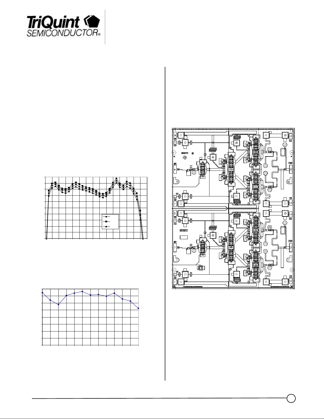
TGA9092-EPU Measured S21 Data
30.00
28.00
26.00
24.00
22.00
20.00
Gain (dB)
18.00
16.00
14.00
12.00
10.00
5 6 7 8 9 10 11 12 13 14 15 16 17 18 19 20
Frequency (GHz)
Mean
+1std
-1std
Primary Applications
• X-Ku band Power
• Point-to-Point Radio
• VSAT
Typical Measured Small Signal Gain
TGA9092-EPU Average Pout
36.00
34.00
32.00
30.00
28.00
Pout (dBm)
26.00
24.00
22.00
20.00
6 7 8 9 10 11 12 13 14 15 16 17 18
RF Probe Data
Chip Dimensions 4.32mm x 5.64mm x 0.100mm
Frequency (GHz)
Typical Measured Pout (RF Probe)
Note: Devices designated as EPU are typically early in their characterization process prior to finalizing all electrical and process
specifications. Specifications are subject to change without notice.
TriQuint Semiconductor Texas : Phone (972)994 8465 Fax (972)994 5804 Web: www.triquint.com
1
Advance Product Information
I+Positive Supply Current
3.5 A
3
/
D
PINInput Continuous Wave Power
25 dBm
CH
M
T
STG
Storage Temperature
P1-14
BV
GS1
Breakdown Voltage gate-source
-30-8V
BV
GD1-3
Breakdown Voltage gate-drain
-30-8V
GpSmall-signal
Power Gain
F = 6 to 18 GHz
212531dBP
3dB
Output Power
@ 3dB gain
compression
F = 6 to 9 GHz
F = 10 to 17 GHz
F = 18 Ghz
303330323433---
dBm
PAE
Power Added
Efficiency
F = 6 to 18 GHz
12
25-%
Note: RF probe data taken at 1GHz steps
Table I
RECOMMENDED MAXIMUM RATINGS
Symbol Parameter Value Notes
+
V
Positive Supply Voltage 9 V
P
T
T
Power Dissipation 25 Watts
Operating Channel Temperature
Mounting Temperature (30 seconds)
150 °C
320 °C
1/, 2/
-65 °C to 150 °C
1/ These ratings apply to each individual FET
2/ Junction operating temperature will directly affect the device mean time to failure
(MTTF). For maximum life it is recommended that junction temperatures be
maintained at the lowest possible levels.
3/ Total current for both channels
Table II
DC PROBE TESTS
(TA = 25 °C ± 5°C)
Symbol Parameter Minimum Maximum Value
V
Pinch-off Voltage -1.5 -0.5 V
Table III
ON-WAFER RF PROBE CHARACTERISTICS
(TA = 25 °C ± 5°C)
Symbol Parameter Test Condition
Limit
Units
Vd=8V, Id=800mA
Min Nom Max
Note: Devices designated as EPU are typically early in their characterization process prior to finalizing all electrical and process
specifications. Specifications are subject to change without notice.
TriQuint Semiconductor Texas : Phone (972)994 8465 Fax (972)994 5804 Web: www.triquint.com
 Loading...