

TriQuint Semiconductor Inc TGA8810-SCC Datasheet
TGA8810-SCC Gain Block Amplifier
2 to 10-GHz Frequency Range
●
Operates from Single 5 -V Supply
●
Unconditionally Stable
●
17-dB Typical Gain
●
Typical ± 0.6-dB Gain Flatness
●
1,8796 x 1,6510 x 0,1524 mm (0.074 x 0.065 x 0.006 in.)
●
O R , I N C .T R I Q U I N T S E M I C O N D U C T
8810
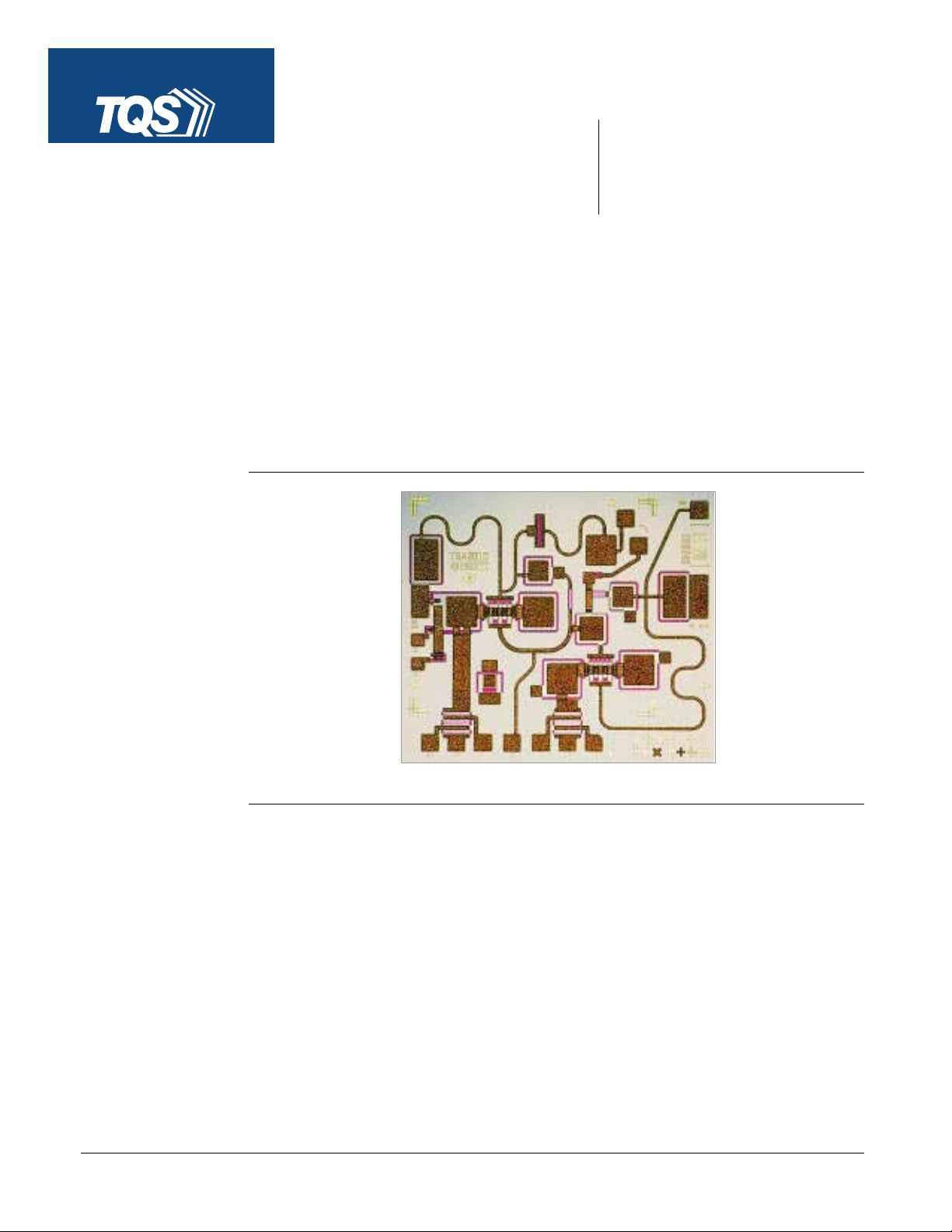
PHOTO ENLARGEMENT
DESCRIPTION
The TriQuint TGA8810
employ shunt feedback to pr oduce flat gain to 10 -GHz. Output power at 1- dB gain compression is
typically 17-dBm and noise figur e is 6-dB. The TGA8810-SCC uses on -chip DC blocks to allow dir ect
cascading. Three dif ferent on-chip self-bias resistors provide the flexibility of selecting bias cur rent
and RF per formance.
-SCC is a self-biased general purpose amplifier. Two gain stages
The TGA8810-SCC is available in chip for m and is readily assembled using automated equipment.
Bond pad and backside metallization is gold plated for compatibil ity with eutectic alloy attachment
methods as well as the ther mocompression and thermosonic wire-bonding processes.
TriQuint Semiconductor, Inc. • Texas Facilities • (972) 995-8465
• www.triquint.com
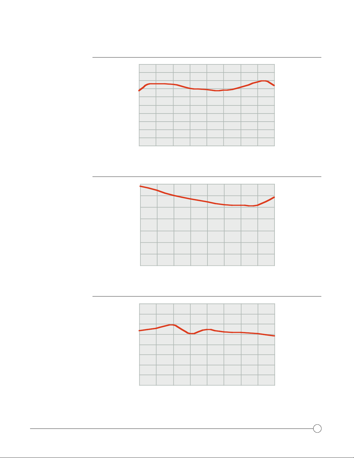
TGA8810-SCC
TYPICAL
SMALL SIGNAL
POWER GAIN
TYPICAL
NOISE FIGURE
20
19
18
17
16
15
Gain (dB)
14
13
12
11
10
23 4567 8910
Frequency (GHz)
7
6
5
4
3
V D1= 5 V
= 5 V
V
D2
= 25° C
T
A
V D1= 5 V
= 5 V
V
D2
= 25° C
T
A
TYPICAL
OUTPUT POWER
P
1dB
Noise Figure (dB)
2
1
0
2345678910
Frequency (GHz)
20
19
18
17
16
15
Output Power (dBm)
14
13
12
23 4567 8910
Frequency (GHz)
V D1= 5 V
= 5 V
V
D2
= 25° C
T
A
TriQuint Semiconductor, Inc. • Texas Facilities • (972) 995-8465
• www.triquint.com
2
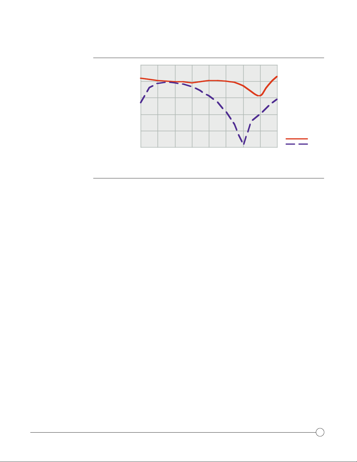
TGA8810-SCC
TYPICAL
RETURN LOSS
ABSOLUTE
MAXIMUM RATINGS
0
10
20
30
V D1= 5 V
= 5 V
V
D2
= 25° C
T
A
Return Loss (dB)
40
Input
50
23 4567 8910
Output
Frequency (GHz)
Positive supply voltage, V
, VD2........................................................................................................ 8.5 V
D1
Power dissipation at (or below) 25°C base -plate temperature, PD* ...................................................... 2.4 W
Operating channel temperature, TCH** .............................................................................................. 150°C
Mounting temperature (30 sec), TM.................................................................................................. 320°C
Storage temperature range, T
Ratings over channel temperature range, TCH(unless otherwise noted)
............................................................................................-65 to 150°C
STG
Stresses beyond those listed under “Absolute Maximum Ratings” m ay cause permanent damage to the device.
These are stress ratings only, and functional operation of the device at these or any oth er conditions beyond
those indicated under “RF Characteristics” is not implied. E xposure to absolute maximum rated conditions for
extended periods may af fect device r eliability.
* For operation above 25°C base -plate temperature, derate linearly at the rate of 5 mW/°C.
** Operating channel temperature, T
, directly af fects the device MTTF. For maximum life, it is r ecommended
CH
that channel temperature be maintained at the lowest possible level.
TriQuint Semiconductor, Inc. • Texas Facilities • (972) 995-8465
• www.triquint.com
3
 Loading...