

TriQuint Semiconductor Inc TGA8310-SCC Datasheet
T R I Q U I N T S E M I C O N D U C T O R , I N C .
TGA8310-SCC Low-Noise Amplifier
8310
2 to 20-GHz Frequency Range
●
3.5- dB Noise Figur e Midband
●
1.4:1 Typical Input/Output SWR
●
17.5- dBm Output Power at 1- dB Gain Compr ession
●
9- dB Typical Gain
●
4,115 x 2,362 x 0,102 mm (0.162 x 0.093 x 0.004 in.)
●
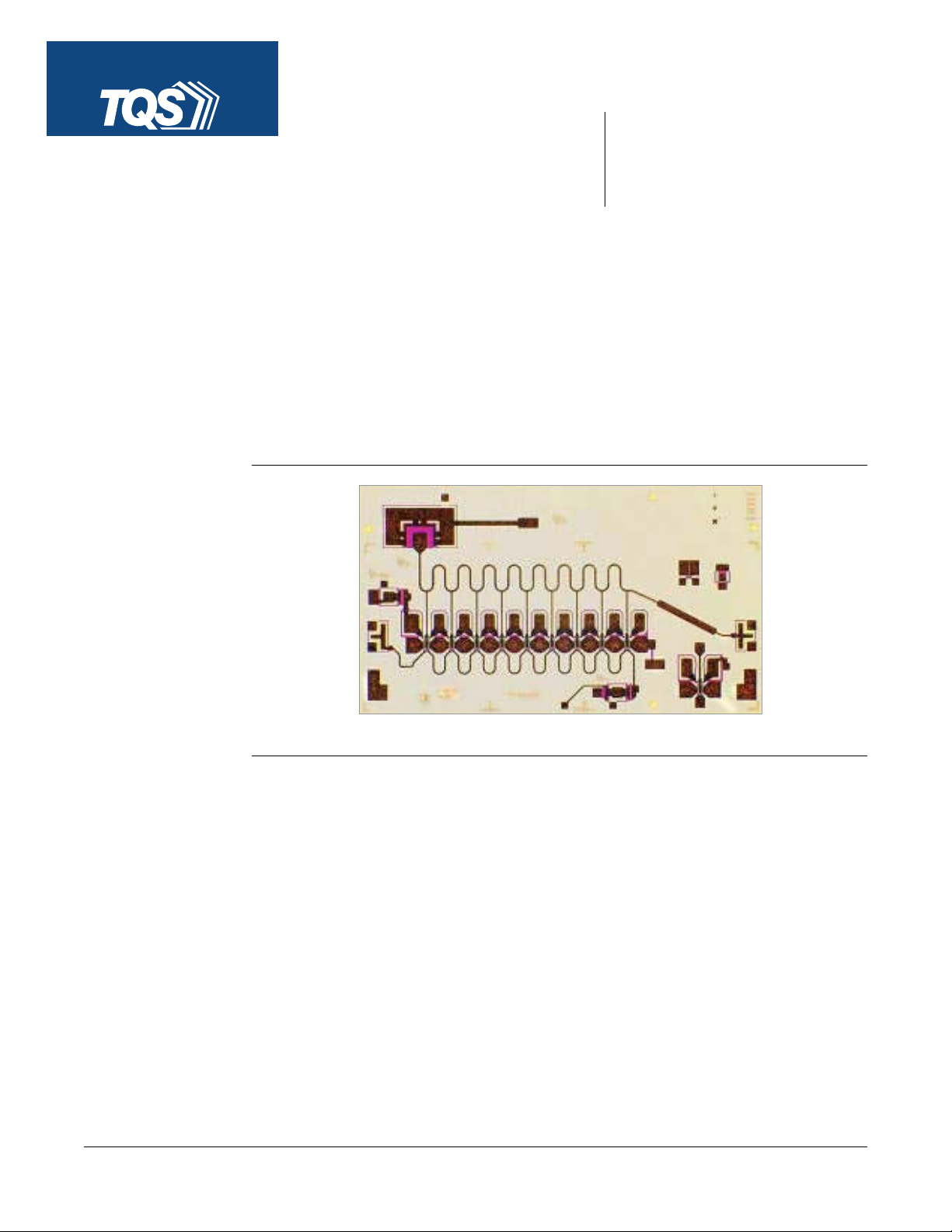
PHOTO ENLARGEMENT
DESCRIPTION
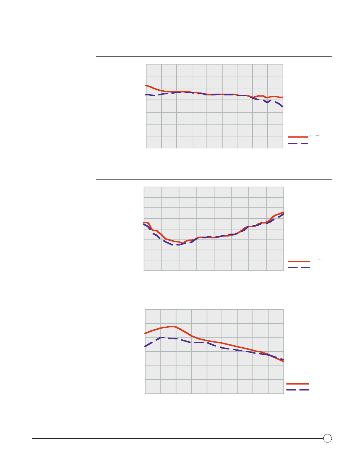
The TriQuint TGA8310 - SCC is a monolithic low - noise distributed amplifier, which operates
from 2 to 20- GHz. Noise figure is typically 4 - dB. Nine 122- µm gatewidth FETs typically provide
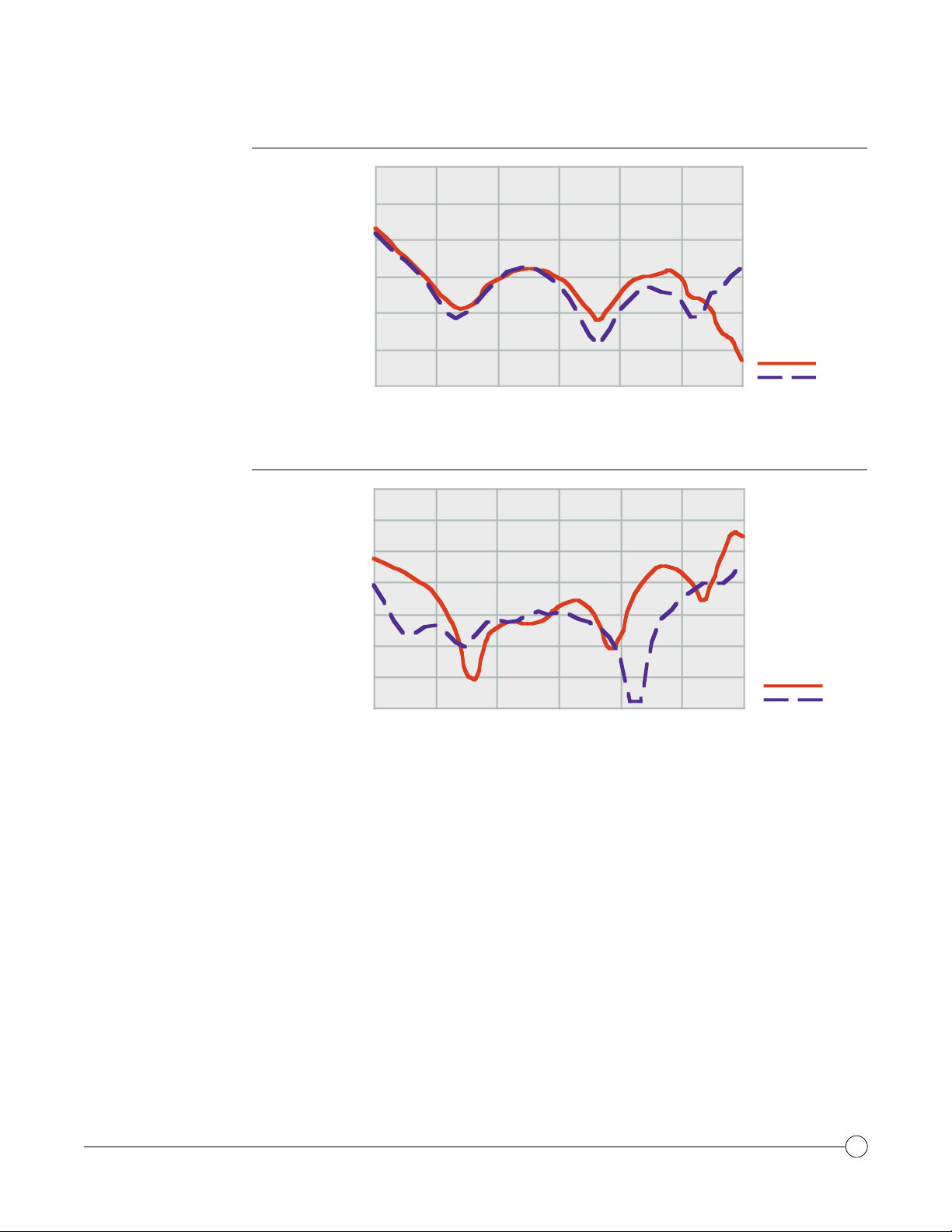
17.5- dBm of output power at 1 - dB gain compression and 9 - dB typical small signal gain. Typical input
return loss is 17-dB from 2 to 20-GHz. Typical output return loss is 20-dB. Ground is provided to
the circuitry through vias to the backside metallization.
The TGA8310 - SCC low - noise distributed amplifier is suitable for a variety of wide - band electr onic
warfare systems such as radar warning receivers, electronic counter-measures, decoys, jammers, and
phased array systems.
Bond pad and backside metallization is gold plated for compatibility with eutectic alloy attachment
methods as well as the thermocompression and ther mosonic wir e - bonding processes. The
TGA8310 - SCC is supplied in chip form and is readily assembled using automated equipment.
TriQuint Semiconductor, Inc. • Texas Facilities • (972) 995-8465
• www.triquint.com
yg
TGA8310-SCC
TYPICAL
SMALL-SIGNAL
POWER GAIN
TYPICAL
NOISE FIGURE
14
12
10
8
6
Gain (dB)
4
2
0
2 4 6 8 10 12 14 16 18 20
Frequency (GHz)
8
7
6
5
4
V
= 1.5 V
CTRL
V
= 1.5 V
CTRL
+
= 60 mA
I
+
= 60 mA
I
= 25°C
T
A
T A= 25° C
V
= 1.5 V
CTRL
V
= 1.5 V
CTRL
+
+
= 60 mA
I
= 60 mA
I
= 25°C
T
T A= 25° C
A
VD = 5V
VD= 5 V
Vd = 5 V
+
+
V
= 8 V
= 8V
V
V+ = 8 V
TYPICAL
OUTPUT POWER
P
1dB
3
Noise Figure (dB)
2
1
0
2 4 6 8 10 12 14 16 18
Frequency (GHz)
22
20
18
16
14
Output Power (dBm)
12
10
2468101214161820
Frequency (GHz)
V
= 1.5 V
CTRL
V
= 1.5 V
CTRL
+
+
= 60 mA
I
= 60 mA
I
= 25°C
T
T A= 25° C
A
Vd = 5V
VD= 5 V
Vd = 5 V
+
+
V
= 8 V
V+ = 8 V
= 8V
V
Vd = 5V
VD= 5 V
Vd = 5 V
+
+
V
= 8 V
= 8V
V
V+ = 8 V
TriQuint Semiconductor, Inc. • Texas Facilities • (972) 995-8465
• www.triquint.com
2
TGA8310-SCC
TYPICAL
INPUT RETURN LOSS
TYPICAL
OUTPUT RETURN LOSS
0
6
12
18
24
Input Return Loss (dB)
30
36
2 5 8 11141720
Frequency (GHz)
0
6
12
18
24
V
= 1.5 V
CTRL
V
= 1.5 V
CTRL
+
+
= 60 mA
I
= 60 mA
I
T A= 25°C
= 25°C
T
A
V
= 1.5 V
CTRL
V
= 1.5 V
CTRL
+
= 60 mA
I
+
I
= 60 mA
= 25°C
T
A
T A= 25°C
VD= 5 V
Vd = 5 V
+
V
= 8 V
V+ = 8 V
30
Output Return Loss (dB)
36
42
2 5 8 11141720
Frequency (GHz)
VD= 5 V
Vd = 5 V
+
V
= 8 V
V+ = 8 V
TriQuint Semiconductor, Inc. • Texas Facilities • (972) 995-8465
• www.triquint.com
3

TGA8310-SCC
ABSOLUTE
MAXIMUM RATINGS
Drain supply voltage, VD ........................................................................................................................
Positive supply voltage, V+..................................................................................................................
Positive supply voltage range with respect to negative supply voltage, V+Positive supply voltage range with respect to gain control voltage, V
Negative supply voltage range, V
Gain control voltage range, V
..............................................................................................
G1
................................................................................................
CTRL
V
..............................
G1
-
V+ ..............................
CTR L
0 V to -13 V
Drain supply current, ID ........................................................................................................................
Positive supply current, I+ ..............................................................................................................
Power dissipation, PD, at (or below) 25 C base-plate temperature* ......................................................
Input continuous wave power, P
....................................................................................................
IN
Operating channel temperature, TCH** ..............................................................................................
Mounting temperature (30 sec), TM ....................................................................................................
Storage temperatur e range, T
Ratings over operating channel temperature range, TCH(unless otherwise noted)
............................................................................................
STG
-
65 to 150 C
9V
12 V
0 V to 13 V
-
5V to 0V
-
5V to 4V
I
188 mA
2.6 W
23 dBm
150 C
320 C
Stresses beyond those listed under “Absolute Maximum Ratings” may cause permanent damage to the device.
These are stress ratings only, and functional operation of the device at these or any other conditions beyond
those indicated under “RF Characteristics” is not implied. Exposure to absolute maximum rated conditions for
extended periods may affect device reliability.
* For operation above 25 C base - plate temperature, derate linearly at the rate of 5.5 mW/ C.
** Operating channel temperature directly affects the device MTTF . For maximum life, it is recommended that
channel temperature be maintained at the lowest possible level.
DSS
TriQuint Semiconductor, Inc. • Texas Facilities • (972) 995-8465
• www.triquint.com
4
 Loading...