

TriQuint Semiconductor Inc TGA8300-SCC Datasheet

T R I Q U I N T S E M I C O N D U C T O R , I N C .
TGA8300- SCC Gain Block Amplifier
8300
2 to 18-GHz Fr equency Range
●
PHOTO ENLARGEMENT
20- dBm Typical Output Power at 1
●
7.5-dB Typical Gain
●
Input/Output SWR 1.5:1
●
On - Chip Blocking Capacitor Allows Easy Cascading
●
2,362 x 1,625 x 0,152 mm (0.093 x 0.064 x 0.006 in.)
●
-dB Gain Compression
DESCRIPTION
TriQuint Semiconductor, Inc. • Texas Facilities • (972) 995-8465
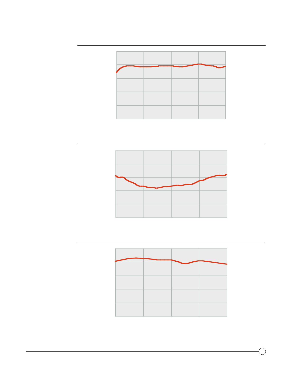
The TriQuint TGA8300 - SCC is a GaAs monolithic distributed amplifier designed for use as a
multioctave general - purpose gain block. Four 189 - µm gate width FETs provide 7.5 -dB nominal gain
and 5.5- dB noise figur e from 2 to 18- GHz. Typical power output is 20 - dBm at 1-dB gain compression.
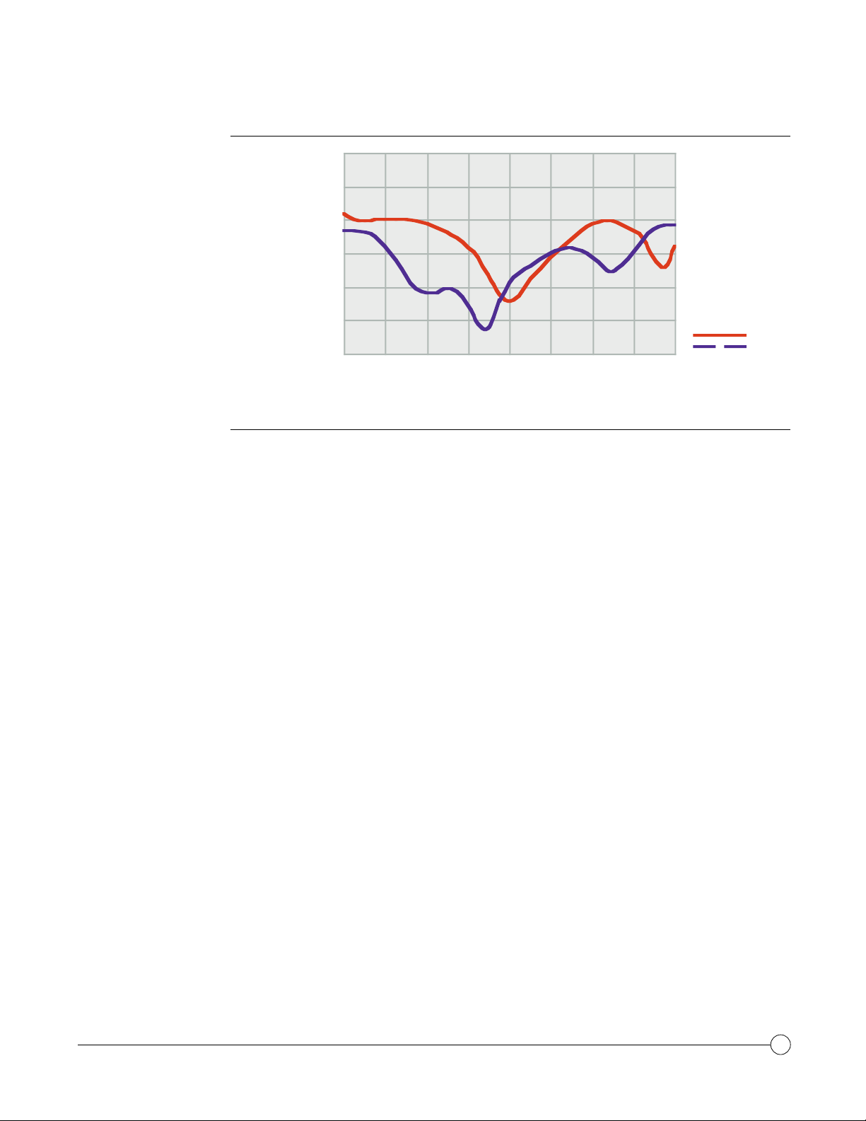
Typical input and output SWRs are 1.5:1. Ground is provided to the circuitry through vias to the
backside metallization.
The TGA8300 - SCC is supplied in chip for m and is engineered for high -volume automated assembly .
All metal sur faces are gold plated to be compatible with ther mocompression and thermosonic
wire - bonding processes.
• www.triquint.com
TGA8300-SCC
TYPICAL
SMALL-SIGNAL
POWER GAIN
TYPICAL
NOISE FIGURE
10
8
6
4
Gain (dB)
2
0
2 6 10 14 18
Frequency (GHz)
10
8
6
V+= 6 V
V+= 6 V
+
+
= 50% I
I
= 50% I
I
TA= 25°C
T A=25° C
V+= 6 V
V+= 6 V
+
+
= 50% I
I
= 50% I
I
T A=25° C
TA= 25°C
DSS
DSS
DSS
DSS
TYPICAL
OUTPUT POWER
P
1dB
4
Noise Figure (dB)
2
0
2 6 10 14 18
Frequency (GHz)
25
20
15
10
Output Power (dBm)
5
0
2 6 10 14 18
Frequency (GHz)
V+= 6 V
V+= 6 V
+
+
= 50% I
I
= 50% I
I
T A=25° C
TA= 25°C
DSS
DSS
TriQuint Semiconductor, Inc. • Texas Facilities • (972) 995-8465
• www.triquint.com
2
TGA8300 -SCC
TYPICAL
RETURN LOSS
ABSOLUTE
MAXIMUM RATINGS
0
6
12
18
24
Return Loss (dB)
30
36
2 4 6 8 10 12 14 16 18
V+= 6 V
V += 6 V
+
+
= 50% I
I
= 50% I
I
T A=25° C
TA= 25°C
DSS
DSS
Input
Input
Output
Output
Frequency (GHz)
Positive supply voltage, V+ .................................................................................................................... 8 V
Negative supply voltage range, V–.............................................................................................. 0 V to -5 V
Power dissipation, PDat (or below) 25 C base-plate temperatur e* ...................................................... 1.8 W
Operating channel temperature, TCH** ......................................................... .....................................150 C
Mounting temperature (30 sec), TM .................................................................................................... 320 C
Storage temperature range, T
Ratings over operating channel temperature range, T
............................................................................................-65 to 150 C
STG
(unless otherwise noted)
CH
Stresses beyond those listed under “Absolute Maximum Ratings” may cause per manent damage to the device.
These are stress ratings only, and functional operation of the device at these or any oth er conditions beyond
those indicated under “RF Characteristics” is not implied. Exposure to absolute maximum rated conditions for
extended periods may affect device reliability.
* For operation above 25 C base-plate temperature, derate linearly at the rate of 3.8 mW/ C.
** Operating channel temperatur e directly affects the device MTTF . For maximum life, it is r ecommended that
channel temperature be maintained at the lowest possible level.
TriQuint Semiconductor, Inc. • Texas Facilities • (972) 995-8465
• www.triquint.com
3
 Loading...