

TriQuint Semiconductor Inc TGA8061-SCC Datasheet
Product Data Sheet
.1 - 3.5 GHz Low Noise Amplifier TGA8061-SCC
Key Features and Performance
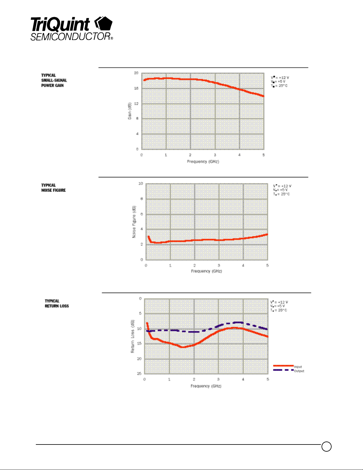
• 100 MHz to 3.5 GHz Frequency Range
• 3 dB Bandwidth Exceeds 5 Octaves
• 2.4 dB Noise Figure with Low Input and
Output SWR
• 18 dB Gain
• 15 dBm Output Power at 1 dB Gain
Compression
• Operates from Single 12V Supply
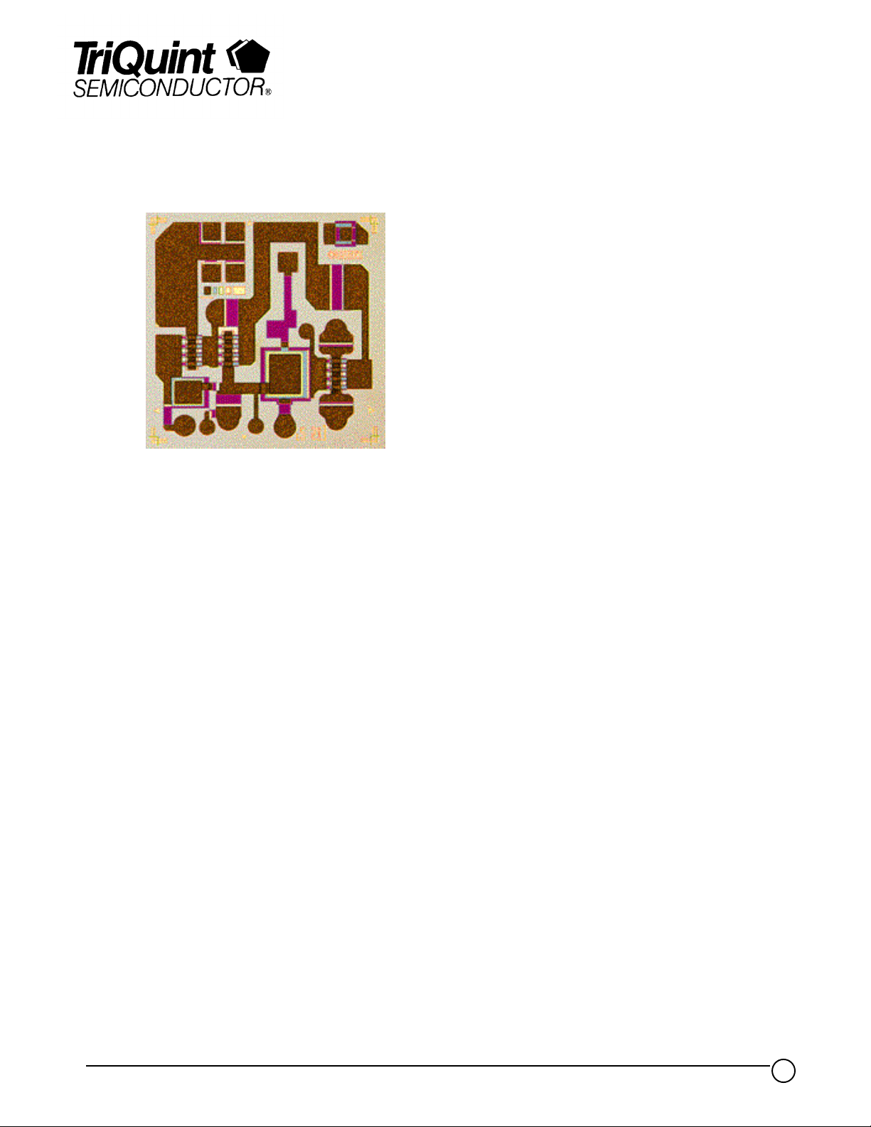
• 1.524 x 1.524 x 0.102 mm (0.060 x 0.060
x 0.004 in.)
Description
The TriQuint TGA8061-SCC is a GaAs monolithic low noise amplifier intended for
use as a universal gain block in applications requiring simultaneous flat gain, low
noise figure, and low SWR over a very wide bandwidth. Three FET stages with
resistive feedback maintain highly repeatable linear phase and amplitude
characteristics.
The high isolation, low SWR, and unconditional stability of the TGA8061-SCC make
it ideal for following or driving mixers and filters. Small size and low external parts
count simplify system design and integration into higher-level assemblies.
Bond pad and backside metallization is gold plated for compatibility with eutectic
alloy attachment methods as well as thermocompression and thermosonic wire
bonding processes. Ground is provided to the circuit through vias to the backside
metallization.
TriQuint Semiconductor Texas Phone: (972)994 8465 Fax: (972)994 8504 Web: www.triquint.com
1
Product Data Sheet
TGA8061-SCC
TriQuint Semiconductor Texas Phone: (972)994 8465 Fax: (972)994 8504 Web: www.triquint.com
2
Product Data Sheet
A
…
M
TGA8061-SCC
ABSOLUTE
MAXIMUM RATINGS
Positive supply voltage, V+……………………………………………………………………………16 V
Bias control voltage range, V
Positive supply current, I+…..………………………………………………………………………
Pow er dissipation, P
, at (or below) 25oC base-plate temperature *………………………………4.3 W
D
Operating Channel temperature, T
Mounting temperature (30 s ec .), T
Storage temperature range, T
………………………………………………………………………0 V to 15 V
DJ
200 mA
**………………………………………………………………150oC
CH
……………………………………………………………………320oC
………………………………………………………………………-65 to 150oC
STG
Ratings over operating channel temperature range, TCH (unless otherw ise noted).
Stresses beyond those listed under "Absolute Maximum Ratings" may c aus e permanent damage to the device.
These are stress ratings only, and functional operation of the device at these or any other conditions beyond
those indicated under "RF Characteristics" is not implied. Exposure to absolute maximum rated conditions
for extended periods may affect device reliability.
* For operation above 25
o
C base-plate temperature, derate linearly at the rate of 9.1 mW/oC.
** Operating channel temperature directly aff ec ts the dev ice MTTF. For maximum life, it is recommended that
channel temperature be maintained at the low est possible level. These ratings apply to each individual FET.
TriQuint Semiconductor Texas Phone: (972)994 8465 Fax: (972)994 8504 Web: www.triquint.com
3
 Loading...