

TriQuint Semiconductor Inc TGA8035-SCC Datasheet
T R I Q U I N T S E M I C O N D U C T O R , I N C .
TGA8035-SCC Gain Block Amplifier
8035
6 to 18-GHz Frequency Range
●
13-dB Typical Gain
●
2.2:1 Typical Input/Output SWR
●
12.5-dBm Typical Output Power at 1 -dB Gain Compression
●
5-dB Typical Noise Figure
●
2,4892 x 2,0574 x 0,1143 mm (0.098 x 0.081 x 0.0045 in.)
●
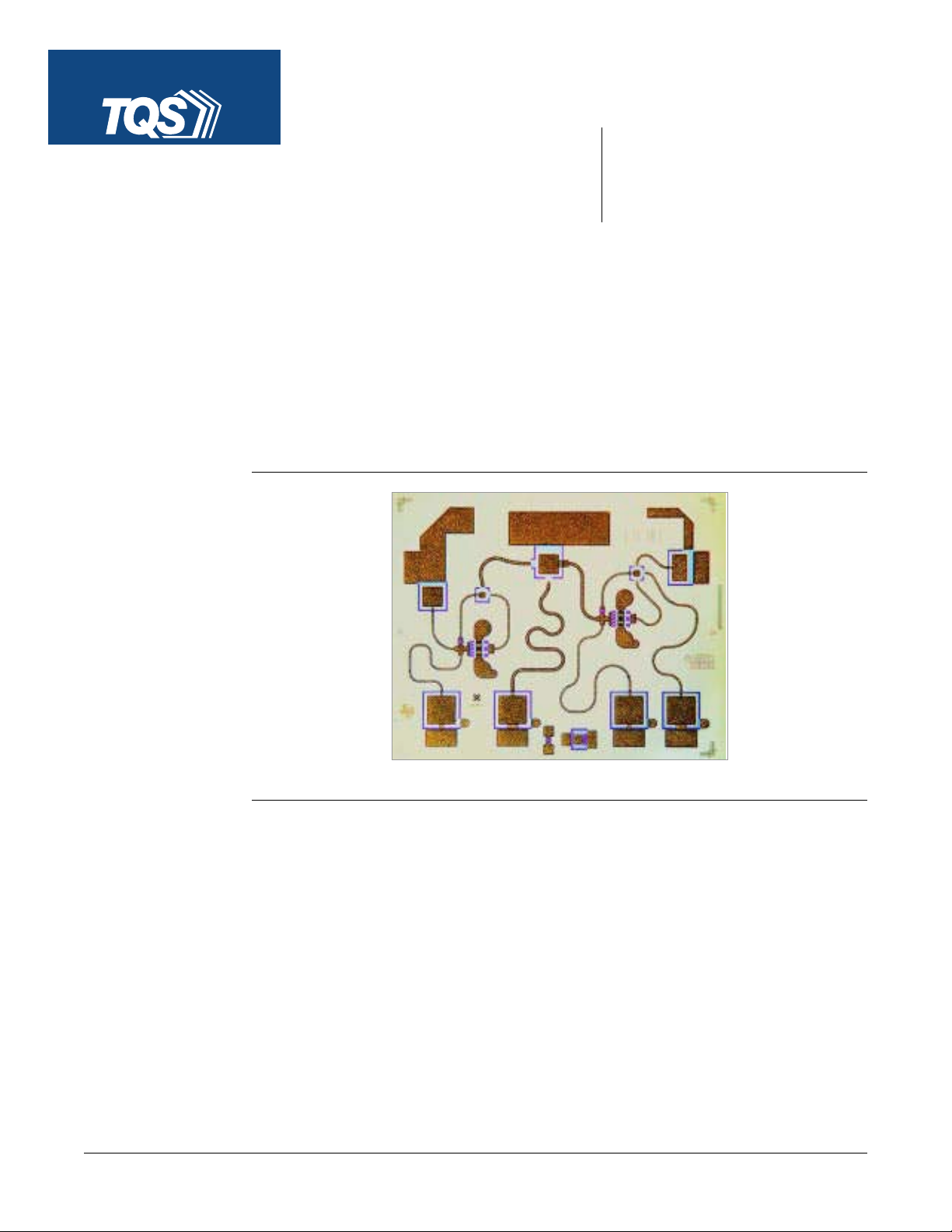
PHOTO ENLARGEMENT
DESCRIPTION
The TriQuint TGA8035 - SCC is a two - stage GaAs monolithic amplifier designed for use as
a broadband general-purpose gain block. T wo 300 - µm gate - width FETs provide a 13- dB typical gain and
a 5- dB noise figure from 6 to 18- GHz. Typical output power at 1- dB gain compression is 12.5 - dBm.
Shunt feedback is used around each active device to improve gain flatness and standing- wave ratio
(SWR). Ground is provided to the circuitry through vias to the backside metallization.
The TGA8035-SCC amplifier is suitable for a variety of broadband electronic warfare (EW) applications.
The combination of gain, power, and noise figure makes this device an exceptional post amplifier
following a low-noise amplifier.
Bond pad and backside metallization is gold plated for compatibility with eutectic alloy attachment
methods as well as thermocompression and thermosonic wire- bonding processes. The TGA8035 - SCC
is supplied in chip form and is readily assembled using automated equipment.
TriQuint Semiconductor, Inc. • Texas Facilities • (972) 995-8465
• www.triquint.com
)
TGA8035-SCC
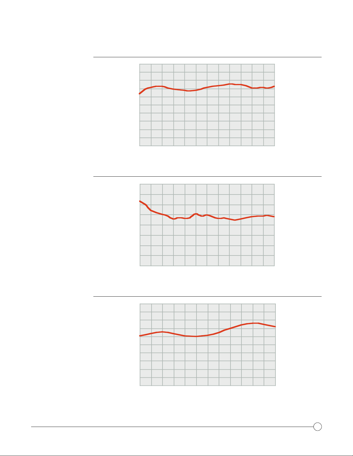
TYPICAL
SMALL-SIGNAL
POWER GAIN
TYPICAL
NOISE FIGURE
20
18
16
14
12
10
8
Gain (dB)
6
4
2
0
6 7 8 9 10 11 12 13 14 15 16 17 18
Frequency (GHz)
8
7
6
5
4
VD1, VD2= 5 V
V D1, V D2= 5 V
= 50% I
I
D1
= 50% I
I
D1
ID2= 50% I
I D2= 50% I
TA= 25°C
T A= 25° C
VD1, VD2= 5 V
V D1, V D2= 5 V
= 50% I
I
= 50% I
I
D1
D1
ID2= 50% I
I D2= 50% I
T A= 25° C
TA= 25°C
DSS1
DSS2
DSS1
DSS2
DSS1
DSS1
DSS2
DSS2
TYPICAL
OUTPUT POWER
P
1dB
3
Noise Figure (dB)
2
1
0
6 7 8 9 10 11 12 13 14 15 16 17 18
Frequency (GHz)
20
18
16
14
12
10
8
6
Output Power (dBm)
4
2
0
6 7 8 9 10 11 12 13 14 15 16 17 18
Frequency (GHz
V D1, V D2= 5 V
VD1, VD2= 5 V
= 50% I
I
D1
= 50% I
I
D1
I D2= 50% I
ID2= 50% I
T A= 25° C
TA= 25°C
DSS1
DSS1
DSS2
DSS2
TriQuint Semiconductor, Inc. • Texas Facilities • (972) 995-8465
• www.triquint.com
2
TGA8035-SCC
TYPICAL
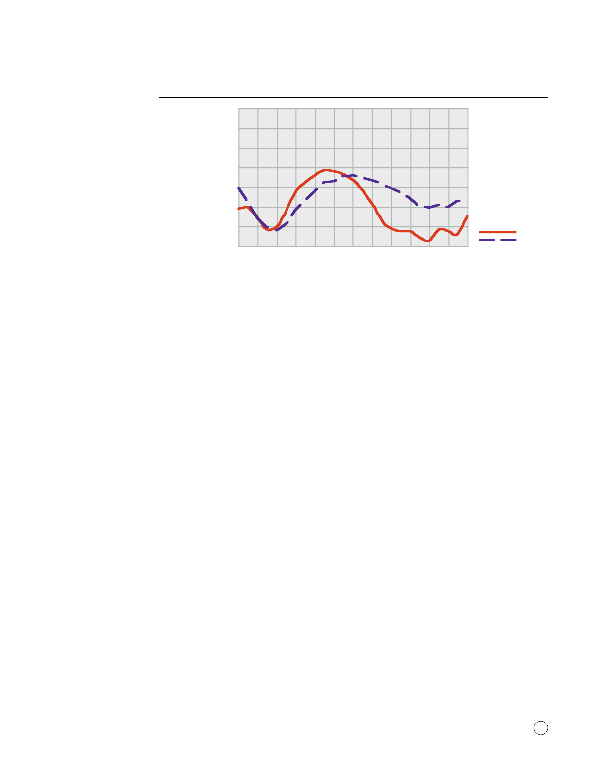
RETURN LOSS
ABSOLUTE
MAXIMUM RATINGS
0
2
VD1, VD2= 5 V
V D1, V D2= 5 V
= 50% I
I
D1
= 50% I
I
D1
ID2= 50% I
I D1= 50% I
TA= 25°C
T A= 25° C
DSS
DSS
DSS1
DSS2
4
6
8
10
Return Loss (dB)
12
14
Input
Input
Output
Output
6 7 8 9 10 11 12 13 14 15 16 17 18
Frequency (GHz)
Drain supply voltage, VD1, V
Drain supply voltage range with respect to negative supply voltage, VD1Negative supply voltage range, V
Positive supply current, I
Positive supply current, I
................................................................................................................ 8 V
D2
VG1, VD2-
, V
...................................................................................... 0 V to -5 V
G1
G2
.................................................................................................................. I
D1
.................................................................................................................. I
D2
VG2.................... 0 V to 8 V
DSS1
DSS2
Power dissipation at (or below) 25 C base-plate temperature, PD* ...................................................... 1.4 W
Input continuous wave power, PIN.................................................................................................... 20 dBm
Operating channel temperature, TCH** .............................................................................................. 150 C
Mounting temperature (30 sec), TM .................................................................................................... 320 C
Storage temperature range, T
Ratings over operating channel temperature range, TCH(unless otherwise noted)
............................................................................................-65 to 150 C
STG
Stresses beyond those listed under “Absolute Maximum Ratings” may cause permanent damage to the device.
These are stress ratings only, and functional operation of the device at these or any other conditions beyond
those indicated under “RF Characteristics” is not implied. Exposure to absolute maximum rated conditions for
extended periods may affect device reliability.
* For operation above 25 C base - plate temperature, derate linearly at the rate of 3 mW/ C.
* Operating channel temperatur e (TCH) directly affects the device MTTF. For maximum life, it is recommended
that channel temperature be maintained at the lowest possible level.
TriQuint Semiconductor, Inc. • Texas Facilities • (972) 995-8465
• www.triquint.com
3
 Loading...