

TriQuint Semiconductor Inc TGA1073G-SCC Datasheet
Product Datasheet
August 15, 2000
19 - 27 GHz Medium Power Amplifier TGA1073G-SCC
Key Features and Performance
• 0.25 um pHEMT Technology
• 22 dB Nominal Gain
• 25 dBm Nominal Pout @ P1dB
• Bias 5-7V @ 220 mA
• Chip Dimensions 2.55 mm x 1.15mm
Primary Applications
The TriQuint TGA1073G-SCC is a three stage
MPA MMIC design using TriQuint’s proven
0.25 um Power pHEMT process. The TGA1073G
is designed to support a variety of millimeter wave
applications including point-to-point digital radio
and point-to-multipoint communications.
The three stage design consists of a 200 um input
device driving a 480um interstage device
followed by an 800um output device.
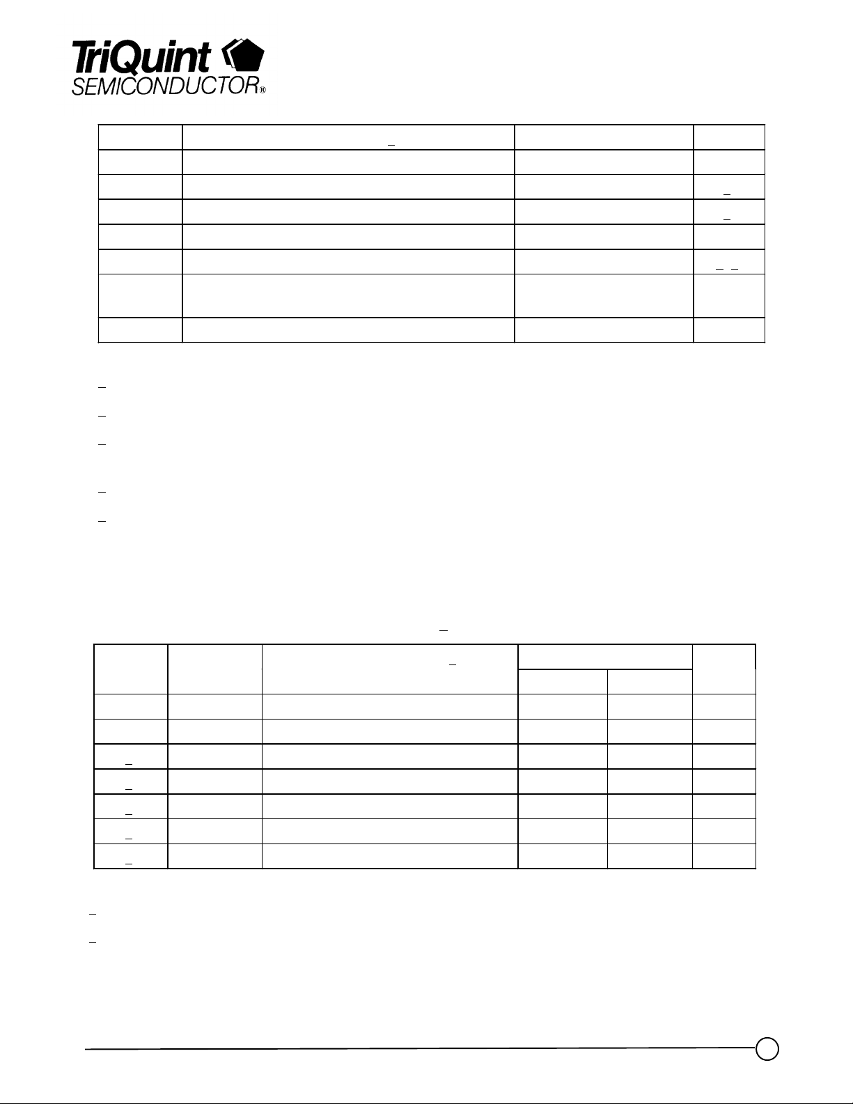
The TGA1073G provides 25dBm nominal
output power at 1dB compression across
19-27GHz. Typical small signal gain is 22 dB.
The TGA91073G requires minimum off-chip
components. Each device is 100% DC and RF
tested on-wafer to ensure performance compliance.
The device is available in chip form.
• Point-to-Point Radio
• Point-to-Multipoint Communications
25
20
15
10
5
0
-5
-10
-15
-20
Gain and Return Loss (dB)
-25
-30
18 19 20 21 22 23 24 25 26 27 28
S21
S11
S22
Frequency (GHz)
28
24
20
16
12
P1dB (dBm)
8
4
0
19 20 21 22 23 24 25 26 27 28 29
Frequency (GHz)
TriQuint Semiconductor Texas : Phone (972)994-8465 Fax (972)994 8504 Web: www.triquint.com
1
rev 11/10/98
Product Datasheet
MAXIMUM RATINGS
August 15, 2000
SYMBOL PARAMETER 5/
+
V
+
I
P
IN
P
D
T
CH
T
M
POSITIVE SUPPLY VOLTAGE 8 V
POSSITIVE SUPPLY CURRENT 296 mA 1/
INPUT CONTINUOUS WAVE POWER 23 dBm 4/
POWER DISSIPATION 2.37 W
OPERATING CHANNEL TEMPERATURE 150 0C2/ 3/
MOUNTING TEMPERATURE
VALUE NOTES
320 0C
(30 SECONDS)
T
STG
STORAGE TEMPERATURE -65 to 150 0C
1/ Total current for all stages.
2/ These ratings apply to each individual FET.
3/ Junction operating temperature will directly affect the device median time to failure (TM). For maximum
life, it is recommended that junction temperatures be maintained at the lowest possible levels.
4/ This value reflects an estimate. Actual value will be inserted as soon as it is determined.
5/ These ratings represent the maximum operable values for the device.
DC SPECIFICATIONS (100%)
= 25 °C + 5 °C)
(T
A
NOTES SYMBOL TEST CONDITIONS 2/ LIMITS UNITS
MIN
I
DSS3
G
M3
STD 80
STD 176
1/ |VP1|STD 0.5
1/ |VP2|STD 0.5
1/ |VP3|STD 0.5
1/ |V
1/ |V
1/ VP, V
BVGD
, and V
|STD 1130V
BVGD1
|STD 1130V
BVGS1
are negative.
BVGS
MAX
376
424
1.5
1.5
1.5
2/ The measurement conditions are subject to change at the manufacture’s discretion (with appropriate
notification to the buyer).
mA
mS
V
V
V
TriQuint Semiconductor Texas : Phone (972)994-8465 Fax (972)994 8504 Web: www.triquint.com
2
rev 11/10/98
 Loading...