

TriQuint Semiconductor Inc TGA1073C-SCC Datasheet
Product Datasheet
r
y
5
pp
B
42526
62728
E
%23
0
4
4Inp
A225240260
August 15, 2000
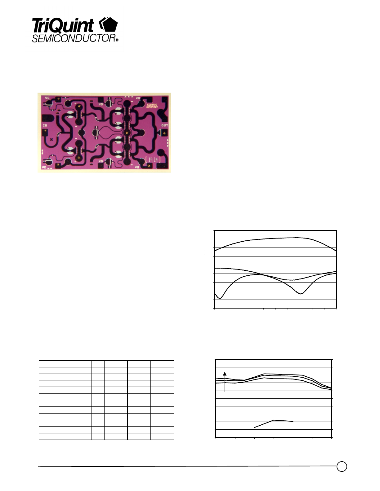
36 - 40 GHz Power Amplifier TGA1073C-SCC
Key Features and Performance
• 0.25um pHEMT Technology
• 36-40 GHz Frequency Range
• 26 dBm Nominal Pout @ P1dB, 38GHz
• 15 dB Nominal Gain
• Bias 5-7V @ 240 mA
• Chip Dimensions 2.4 mm x 1.45 mm
Primary Applications
• Point-to-Point Radio
The TriQuint TGA1073C-SCC is a two stage PA MMIC
design using TriQuint’s proven 0.25 µm Power pHEMT
process to support a variety of millimeter wave
applications including point-to-point digital radio and
point-to-multipoint systems.
The two-stage design consists of two 400 µm input
devices driving four 400 µm output devices.
The TGA1073C provides 24 dBm of output power at
1dB gain compression and 26 dBm saturated output
power across the 36-40 GHz with a typical small signal
gain of 15 dB.
The TGA1073C requires a minimum of off-chip
components. Each device is 100% DC and RF tested
on-wafer to ensure performance compliance. The
device is available in chip form.
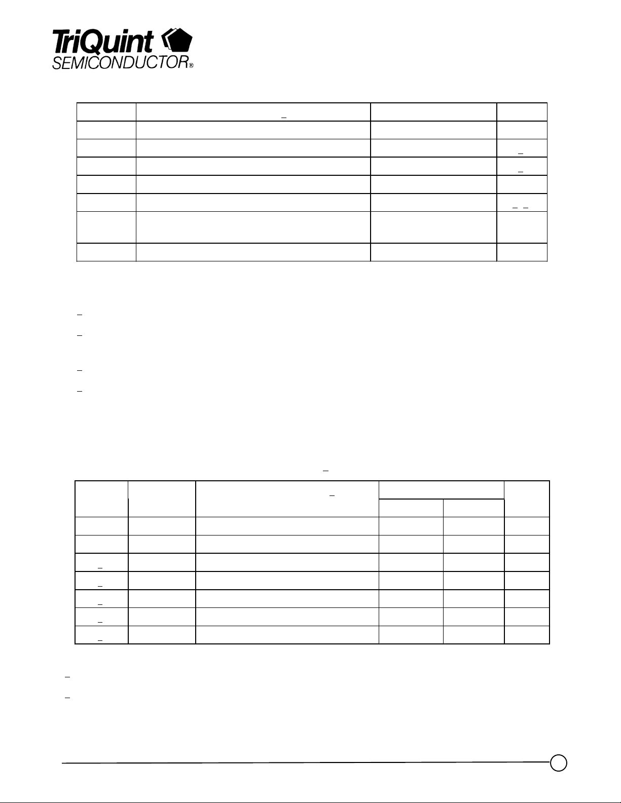
Typical Performance, 36-40 GHz
Paramet e
Small Signal Gain dB 1
Gain Flatness dB
Output P1d
Saturated Output Power dBm 2
Saturated PA
Output OTOI dBm 3
IMR3 @ SCL = P1dB - 10dB dBc 3
ut Ret urn Loss dB -10
Output Ret urn Loss dB -8
Reverse Isolati on dB -35
Quiescent Current m
Unit +5V Supply+6V Supply+7V Suppl
1
dBm 2
22 2
• Point-to-Multipoint Radio
TGA1073C Typical RF Performance (Fixtured)
20
15
10
5
0
-5
-10
-15
Gain and Return Loss (dB)
-20
-25
33 34 35 36 37 38 39 40 41 42 43
33
30
27
24
21
18
15
12
9
6
Output Power @ P1dB (dBm)
3
36 37 38 39 40 41 42
S22
S11
Frequency (GHz)
TGA1073C Typical RF Performance (Fixtured)
P1dB
VD = +5V, +6V, +7V
IMR3 @ VD = +6V
Frequency (GHz)
S21
50
48
46
44
42
40
38
36
34
32
IMR3 @ SCL=P1dB-10dB (dBc)
30
TriQuint Semiconductor Texas : (972)994 8465 Fax (972)994 8504 Web: www.triquint.com
1
MAXIMUM RATINGS
Product Datasheet
TGA1073C-SCC
SYMBOL PARAMETER 5/
+
V
+
I
P
IN
P
D
T
CH
T
M
POSITIVE SUPPLY VOLTAGE 8 V
POSITIVE SUPPLY CURRENT 480 mA 1/
INPUT CONTINUOUS WAVE POWER 23 dBm 4/
POWER DISSIPATION 3.84 W
OPERATING CHANNEL TEMPERATURE 150 0C2/ 3/
MOUNTING TEMPERATURE
VALUE NOTES
320 0C
(30 SECONDS)
T
STG
STORAGE TEMPERATURE -65 to 150 0C
1/ Total current for all stages.
2/ These ratings apply to each individual FET.
3/ Junction operating temperature will directly affect the device median time to failure (TM). For maximum
life, it is recommended that junction temperatures be maintained at the lowest possible levels.
4/ This value reflects an estimate. Actual value will be inserted as soon as it is determined.
5/ These ratings represent the maximum operable values for this device.
DC SPECIFICATIONS (100%)
= 25 °C + 5 °C)
(T
A
NOTES SYMBOL TEST CONDITIONS 2/ LIMITS UNITS
MAX
188
212
1.5
1.5
1.5
mA
mS
V
V
V
1/ |VP1|STD 0.5
1/ |VP2|STD 0.5
1/ |V
1/ |V
1/ |V
1/ VP, V
BVGD
I
G
BVGD1,2
BVGS1
, and V
MIN
DSS1
M1
|STD 0.5
P3-6
STD 40
STD 88
|STD 1130V
|STD 1130V
are negative.
BVGS
2/ The measurement conditions are subject to change at the manufacture’s discretion (with appropriate notification to
the buyer).
TriQuint Semiconductor Texas : (972)994 8465 Fax (972)994 8504 Web: www.triquint.com
2
 Loading...