

TriQuint Semiconductor Inc TGA1073A-SCC Datasheet
Product Datasheet
August 15, 2000
26- 34 GHz Medium Power Amplifier TGA1073A-SCC
Key Features and Performance
• 0.25 um pHEMT Technology
• 19 dB Nominal Gain
• 25 dBm Nominal Pout @ P1dB
• -34.5 dBc IMR3 @ 15.5 dBm SCL
• Bias 5 - 7V @ 220 mA
• Chip Dimensions 1.95 mm x 1.12 mm
Primary Applications
• Point-to-Point Radio
The TriQuint TGA1073A-SCC is a three stage
MPA MMIC design using TriQuint’s proven
0.25 um Power pHEMT process. The TGA1073A
is designed to support a variety of millimeter wave
applications including point-to-point digital radio
and LMDS/LMCS.
The three stage design consists of a 200 um input
device driving a 480um interstage device
followed by an 800um output device.
The TGA1073A provides 25dBm nominal
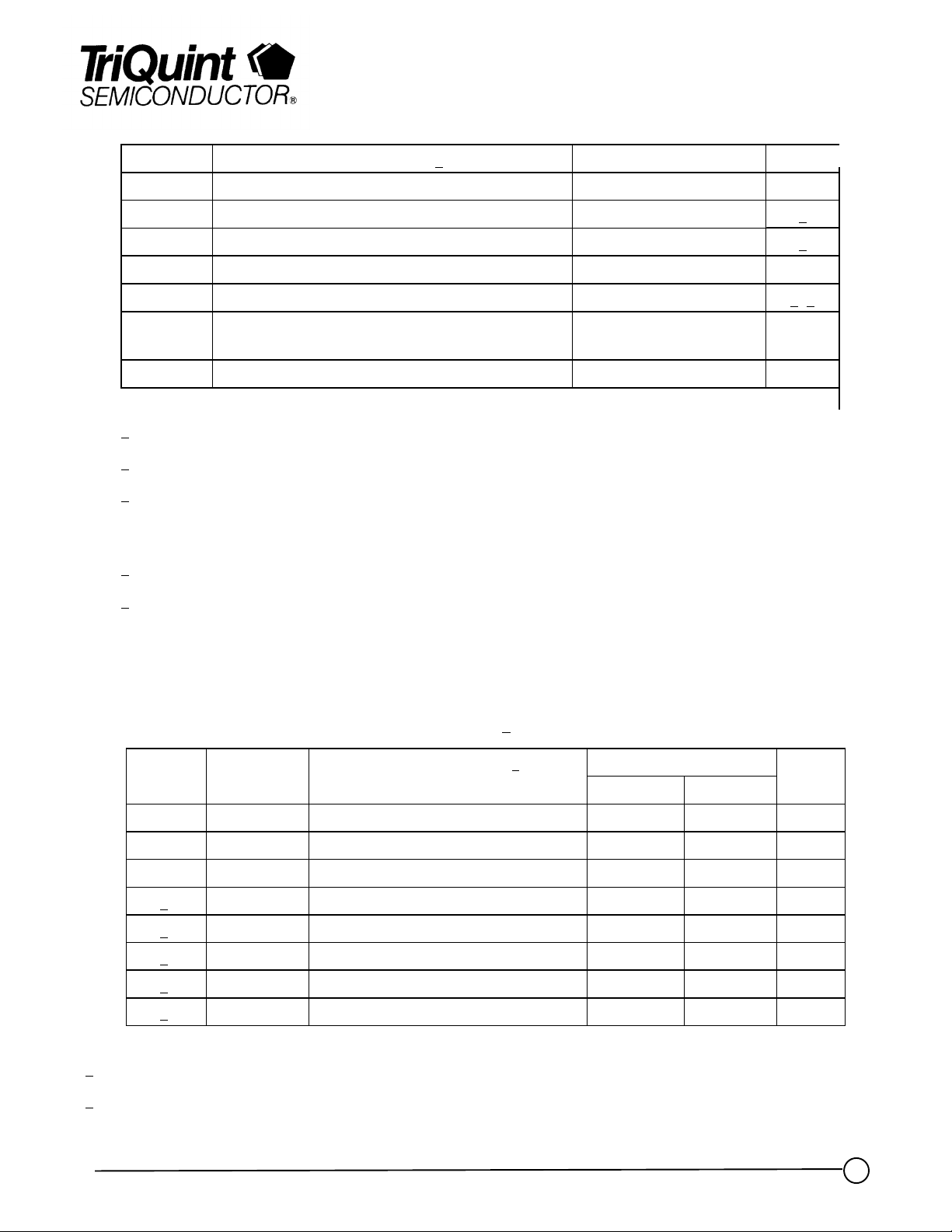
output power at 1dB compression across
26-34GHz. Typical small signal gain is 19 dB.
The TGA1073A requires minimum off-chip
components. Each device is 100% DC and RF
tested on-wafer to ensure performance compliance.
The device is available in chip form.
• Point-to-Multipoint Communications
• LMDS CPE PA
25
20
15
10
5
0
-5
-10
Gain and Return Loss (dB)
-15
-20
26 27 28 29 30 31 32 33 34
S21
S11
S22
Frequency (GHz)
30
25
20
15
10
P1dB (dBm)
5
0
26 27 28 29 30 31 32 33 34 35 36
Frequency (GHz)
TriQuint Semiconductor Texas : Phone (972)994-8465 Fax (972)994 8504 Web: www.triquint.com
1
rev 11/10/98
MAXIMUM RATINGS
Product Datasheet
TGA1073A-SCC
SYMBOL PARAMETER 5/
+
V
+
I
P
IN
P
D
T
CH
T
M
POSITIVE SUPPLY VOLTAGE 8 V
POSITIVE SUPPLY CURRENT 296 mA 1/
INPUT CONTINUOUS WAVE POWER 23 dBm 4/
POWER DISSIPATION 2.37 W
OPERATING CHANNEL TEMPERATURE 150 0C2/ 3/
MOUNTING TEMPERATURE
VALUE NOTES
320 0C
(30 SECONDS)
T
STG
STORAGE TEMPERATURE -65 to 150 0C
1/ Total current for all stages.
2/ These ratings apply to each individual FET.
3/ Junction operating temperature will directly affect the device median time to failure (TM). For
maximum life, it is recommended that junction temperatures be maintained at the lowest possible
levels.
4/ This value reflects an estimate. Actual value will be inserted as soon as it is determined.
5/ These ratings represent the maximum operable values for the device.
DC SPECIFICATIONS (100%)
(T
= 25 °C + 5 °C)
A
NOTES SYMBOL TEST CONDITIONS 2/ LIMITS UNITS
MAX
516
376
424
1.5
1.5
1.5
mA
mA
mS
V
V
V
1/ VP, V
MIN
I
MAX3
I
DSS3
G
M3
STD 300
STD 80
STD 176
1/ |VP1|STD 0.5
1/ |VP2|STD 0.5
1/ |VP3|STD 0.5
1/ |V
1/ |V
, and V
BVGD
|STD 1130V
BVGD1
|STD 1130V
BVGS1
are negative.
BVGS
2/ The measurement conditions are subject to change at the manufacture’s discretion (with appropriate notification to the
buyer).
TriQuint Semiconductor Texas : Phone (972)994-8465 Fax (972)994 8504 Web: www.triquint.com
2
rev 11/10/98
RF SPECIFICATIONS
= 25°C + 5°C)
(T
A
Product Datasheet
TGA1073A-SCC
NOTE TEST MEASUREMENT
CONDITIONS
6V @ 220mA
1/
SMALL-SIGNAL
26 – 33 GHz 17 19 dB
GAIN MAGNITUDE
27 GHz 22 24.5 dBmPOWER OUTPUT
AT 1 dB GAIN
COMPRESSION
28 – 33 GHz 23 dBm
26 – 33 GHz -15 dB1/ INPUT RETURN LOSS
2/
MAGNITUDE
OUTPUT RETURN LOSS
MAGNITUDE
OUTPUT THIRD ORDER
28 – 32 GHz -10 dB
26 – 33 GHz -15 dB1/
28 – 32 GHz -10 dB
INTERCEPT
1/ RF probe data is taken at 0.5 GHz steps.
VALUE UNITS
MIN TYP MAX
32 dBm
2/ Minimum output third-order-intercept (OTOI) is generally 6dB minimum above the 1dB compression point (P1dB).
Calculations are based on standard two-tone testing with each tone approximately 10dB below the nominal P1dB.
Factors that may affect OTOI performance include device bias, measurement frequency, operating temperature,
output interface and output power level for each tone.
RELIABILITY DATA
PARAMETER BIAS CONDITIONS P
DISS
R
θJC
T
CH
VD (V) ID (mA) (W) (C/W) (°C) (HRS)
R
Thermal resistance
θJC
6 220 1.32 69.4 146.6 1.3 E6
(channel to backside of c/p)
Note: Assumes eutectic attach using 1.5 mil thick 80/20 AuSn mounted to a 20mil CuMo Carrier at 55°C
baseplate temperature. Worst case condition with no RF applied, 100% of DC power is
dissipated.
T
M
TriQuint Semiconductor Texas : Phone (972)994-8465 Fax (972)994 8504 Web: www.triquint.com
3
rev 11/10/98
 Loading...