

TriQuint Semiconductor Inc TGA1071-EPU Datasheet
36 - 40 GHz Power Amplifier TGA1071-EPU
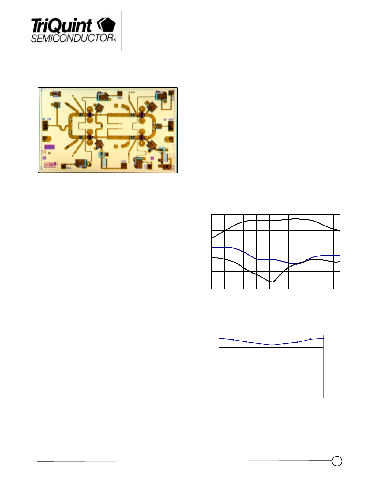
The TriQuint TGA1071-EPU is a two stage
PA MMIC design using TriQuint’s proven
0.25 um Power pHEMT process to support a variety
of millimeter wave applications including
point-to-point digital radio and point-to-multipoint
systems.
The two-stage design consists of two 300 um input
devices driving a pair of 400 um output devices.
The TGA1071 provides 22dBm of output power
across 36-40 GHz with a typical small signal gain
of 15dB.
The TGA1071 requires minimum off-chip
components. Each device is 100% DC and RF
tested on-wafer to ensure performance compliance.
The device is available in chip form.
Advance Product Information
Key Features and Performance
• 0.25um pHEMT Technology
• 36-40 GHz Frequency Range
• 22 dBm Nominal Pout @ P1dB
• 15 dB Nominal Gain
• 5V, 120 mA Bias
• Chip Dimensions 3.4mm x 2.1mm
Primary Applications
• Point-to-Point Radio
• Point-Multipoint Radio
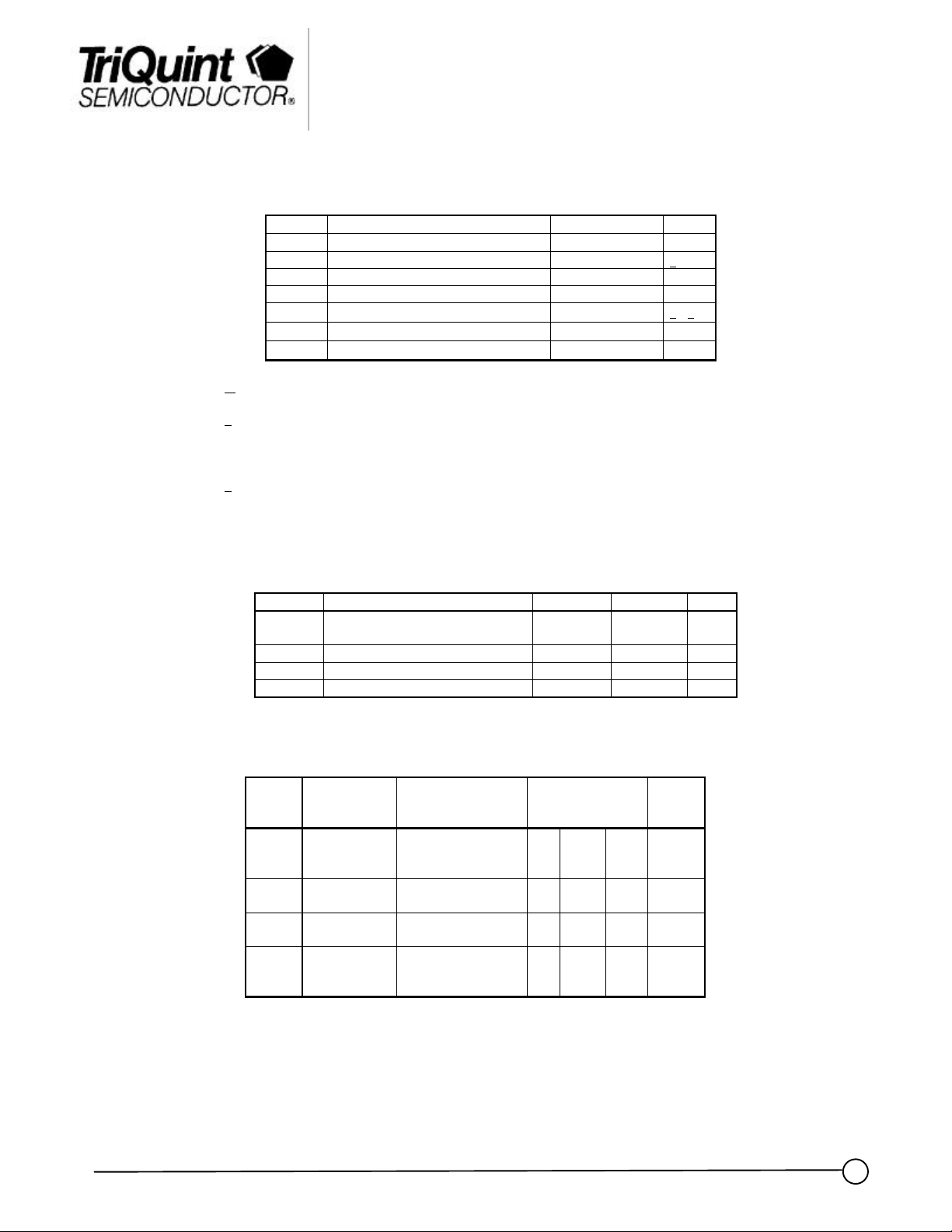
TGA1071 Typical RF Performance (Fixtured)
20
15
10
5
0
-5
-10
Gain and Return Loss (dB)
-15
-20
-25
32.0 33.0 34.0 35.0 36.0 37.0 38.0 39.0 40.0 41.0 42.0
25.00
s11
s22
Frequency (GHz)
Small Signal Gain
TGA1071 RF Probe Summary Data
20.00
15.00
10.00
Pout (dBm)
5.00
0.00
36 37 38 39 40
Frequency (GHz)
Pout at 1dB Gain Compression
Note: Devices designated as EPU are typically early in their characterization process prior to finalizing all electrical and process
specifications. Specifications subject to change without notice
TriQuint Semiconductor Texas : Phone (972)994 8465 Fax (972)994 8504 Web: www.triquint.com
1
1
Advance Product Information
+
D
IN
CH
M
STG
P1-5
GS1
GD1-5
p
Note: RF probe data is taken at 0.4 GHz steps
Electrical Characteristics
RECOMMENDED MAXIMUM RATINGS
Symbol Parameter Value Notes
+
V
I
P
P
T
T
T
1/ These ratings apply to each individual FET
2/ Junction operating temperature will directly affect the device mean time to failure
(MTTF). For maximum life it is recommended that junction temperatures be
maintained at the lowest possible levels.
3/ Total current for both stages
Positive Supply Voltage 7 V
Positive Supply Current .4 A 3/
Power Dissipation 2.8 W
Input Continuous Wave Power 20 dBm
Operating Channel Temperature
Mounting Temperature (30 seconds)
Storage Temperature
150 °C
320 °C
-65 °C to 150 °C
1/, 2/
DC PROBE TESTS
(TA = 25 °C ± 5°C)
Symbol Parameter Minimum Maximum Value
Idss Saturated Drain Current (info
140 658 mA
only)
V
BV
BV
Pinch-off Voltage -1.5 -0.5 V
Breakdown Voltage gate-source -30 -8 V
Breakdown Voltage gate-drain -30 -8 V
ON-WAFER RF PROBE CHARACTERISTICS
(TA = 25 °C ± 5°C)
Symbol Parameter Test Condition
Limit
Units
Vd=5V, Id=120mA
Min Nom Max
G
Small-signal
Power Gain
F = 36 to 40 GHz
F = 38 GHz 13
15 dB
dB
dB
IRL Input Return
F = 36 to 40 GHz - -10 - dB
Loss
ORL Output Return
F = 36 to 40 GHz - -10 - dB
Loss
PWR Output Power F = 36 to 40 GHz 22 - dBm
Note: Devices designated as EPU are typically early in their characterization process prior to finalizing all electrical and process
specifications. Specifications are subject to change without notice.
TriQuint Semiconductor Texas : Phone (972)994 8465 Fax (972)994 8504 Web: www.triquint.com
2
 Loading...