

TriQuint Semiconductor Inc GA1088MC700, GA1088MC500 Datasheet
T R I Q U I N T S E M I C O N D U C T O R , I N C .
1
SYSTEM TIMING
PRODUCTS
For additional information and latest specifications, see our website: www.triquint.com
Output Buffers
VCO
Phase
Detector
VDD
Q10
Q9
GND
Q8
Q7
VDD
TEST
VDD
Q0
GND
Q1
Q2
VDD
FBIN S1 REFCLK S0 F1 F0 GND
GND Q3 Q4 VDD Q5 Q6 GND
1
2
14
13
12
11 10
9
8765
4
3
22212019
18
17
16
15
27
28
252423
26
Phase
Select
MUX
Divide Logic
÷4, ÷6, or ÷8
Group
A
Group B
Group
C
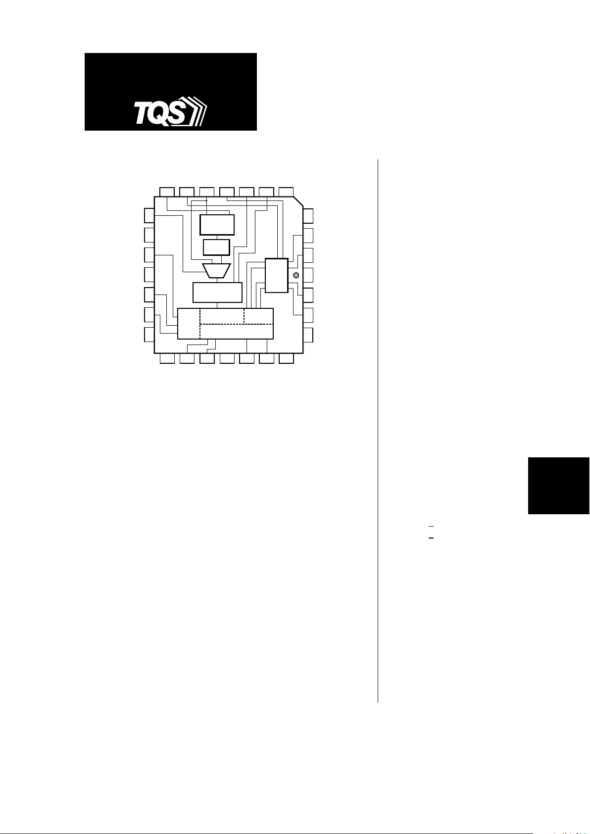
TriQuint’s GA1088 is a configurable clock buffer which generates 11
outputs, operating over a wide range of frequencies — from 18 MHz to
105 MHz. The outputs are available at either 1x and 2x or at 1x and
1
/2 x
the reference clock frequency, f
REF
. When one of the Group A outputs (Q0–
Q2) is used as feedback to the PLL, all Group A outputs will be at f
REF
, and
all Group B (Q3–Q6) and Group C (Q7–Q10) outputs will be at 2x f
REF
.
When one of the Group B outputs is used as feedback to the PLL, all Group
A outputs will be at
1
/2 x f
REF
and all Group B and Group C outputs will
be at f
REF
.
A very stable internal Phase-Locked Loop (PLL) provides low-jitter
operation. This completely self-contained PLL requires no external
capacitors or resistors. The PLL’s voltage-controlled oscillator (VCO) has a
frequency range from 280 MHz to 420 MHz. By feeding back one of the
output clocks to FBIN, the PLL continuously maintains frequency and
phase synchronization between the reference clock (REFCLK) and each of
the outputs. The Shift Select pins select the phase shift (–2t, –t, 0, or +t)
for Group C outputs (Q7–Q10) with respect to REFCLK. The phase shift
increment (t) is equivalent to the VCO’s period (1/f
VCO
).
TriQuint’s patented output buffer design delivers a very low output-tooutput skew of 150 ps (max). The GA1088’s symmetrical TTL outputs are
capable of sourcing and sinking 30 mA.
GA1088
Features
• Wide frequency range:
18 MHz to 105 MHz
• Output configurations:
three outputs at
1
/2 f
REF
three outputs at f
REF
four outputs at f
REF
with adjustable phase or
two outputs at f
REF
four outputs at 2x f
REF
four outputs at 2x f
REF
with adjustable phase
• Selectable Phase Shift:
–2t, –t, 0, and +t (t = 1/f
VCO
)
• Low output-to-output skew:
150 ps (max) within a group
• Near-zero propagation delay
–350 ps
+ 500 ps (max) or
–350 ps
+700 ps (max)
• TTL-compatible with 30 mA
output drive
• 28-pin J-lead surface-mount
package
11-Output
Configurable
Clock Buffer
GA1088
For additional information and latest specifications, see our website: www.triquint.com
2
Functional Description
The core of the GA1088 is a Phase-Locked Loop (PLL)
that continuously compares the reference clock
(REFCLK) to the feedback clock (FBIN), maintaining a
zero frequency difference between the two. Since one
of the outputs (Q0–Q6) is always connected to FBIN,
the PLL keeps the propagation delay between the
outputs and the reference clock within –350 ps
+500 ps
for the GA1088-MC500, and within –350 ps
+700 ps
for the GA1088-MC700.
The internal voltage-controlled oscillator (VCO) has an
operating range of 280 MHz to 420 MHz. The
combination of the VCO and the Divide Logic enables
the GA1088 to operate between 18 MHz and 105 MHz.
The device features six divide modes: ÷4, ÷6, ÷8, ÷8,
÷12, and ÷16. The Frequency Select pins, F0 and F1,
and the output used as feedback to FBIN set the divide
mode as shown in Table 1.
The Shift Select pins, S0 and S1, control the phase
shift of the Group C outputs (Q7–Q10), relative to the
other outputs. The user can select from four
incremental phase shifts as shown in Table 2 (Phase
Selection). The phase-shift increment (t) is calculated
using the following equation (where n is the
divide mode):
In the test mode, the PLL is bypassed and REFCLK is
connected directly to the Divide Logic block via the
MUX, as shown in Figure 1. This mode is useful for
debug and test purposes. The various test modes are
outlined in Table 3. In the test mode, the frequency of
the reference clock is divided by 4, 6, or 8.
The maximum rise and fall time at the output pins is
1.4 ns. All outputs of the GA1088 are TTL-compatible
with 30 mA symmetric drive and a minimum VOH of 2.4 V.
Power Up/Reset Synchronization
After power up or reset, the PLL requires time before it
achieves synchronization lock. The maximum time
required for synchronization (TSYNC) is 500 ms.
Table 1. Frequency Mode Selection
Feedback: Any Group B Output (Q3 – Q6)
Select Pins Reference Clock Output Frequency Range
Test F0 F1 Mode Frequency Range Group A: Q0–Q2 Group B,C: Q3–Q10
0 0 0 Not Used N.A. N.A. N.A.
010 ÷ 8 35 MHz – 50 MHz 35 MHz – 50 MHz 70 MHz – 105 MHz
001 ÷ 12 24 MHz – 35 MHz 24 MHz – 35 MHz 48 MHz – 70 MHz
011 ÷ 16 18 MHz – 26 MHz 18 MHz – 26 MHz 35 MHz – 52 MHz
Feedback: Any Group A Output (Q0 – Q2)
Select Pins Reference Clock Output Frequency Range
Test F0 F1 Mode Frequency Range Group A: Q0–Q2 Group B,C: Q3–Q10
0 0 0 Not Used N.A. N.A. N.A.
010 ÷ 4 70 MHz – 105 MHz 35 MHz – 50 MHz 70 MHz – 105 MHz
001 ÷ 6 48 MHz – 70 MHz 24 MHz – 35 MHz 48 MHz – 70 MHz
011 ÷ 8 35 MHz – 52 MHz 18 MHz – 26 MHz 35 MHz – 52 MHz
t =
1
(f ) (n)
REF
GA1088
3
SYSTEM TIMING
PRODUCTS
For additional information and latest specifications, see our website: www.triquint.com
S0 S1 Phase Difference (Q9, Q10)
00 +t
10 0
01 –t
1 1 –2t
Table 2. Phase Selection
Table 3. Test Mode Selection
Group A: Group B,C
Test F0 F1 Mode Ref. Clock Outputs Q0–Q2 Outputs Q3–Q10
1 0 0 not used — — —
11 0 ÷ 4f
REF
f
REF
÷ 8f
REF
÷ 4␣ ␣
10 1 ÷ 6f
REF
f
REF
÷ 12 f
REF
÷ 6
11 1 ÷ 8f
REF
f
REF
÷ 16 f
REF
÷ 8
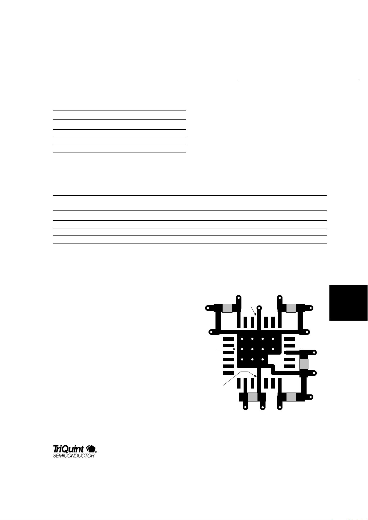
Layout Guidelines
Multiple ground and power pins on the GA1088 reduce
ground bounce. Good layout techniques, however, are
necessary to guarantee proper operation and to meet
the specifications across the full operating range.
TriQuint recommends bypassing each of the V
DD
supply
pins to the nearest ground pin, as close to the chip as
possible.
Figure 2 shows the recommended power layout for the
GA1088. The bypass capacitors should be located on
the same side of the board as the GA1088. The V
DD
traces connect to an inner-layer VDD plane. All of the
ground pins (GND) are connected to a small ground
plane on the surface beneath the chip. Multiple throughholes connect this small surface plane to an inner-layer
ground plane. The capacitors (C1–C5) are 0.1 mF.
TriQuint’s test board uses X7R temperature-stable
capacitors in 1206 SMD cases.
Figure 2. Top Layer Layout of Power Pins (approx. 3.3x)
C4
C5
C1
C2
C3
Pin 1
Pin 15
Ground
Plane
V
DD
V
DD
V
DD
V
DD
V
DD
 Loading...