

TriQuint Semiconductor Inc GA1086MC500, GA1086MC1000 Datasheet
T R I Q U I N T S E M I C O N D U C T O R , I N C .
SYSTEM TIMING
PRODUCTS
1
For additional information and latest specifications, see our website: www.triquint.com
GA1086
11-Output
Clock Buffer
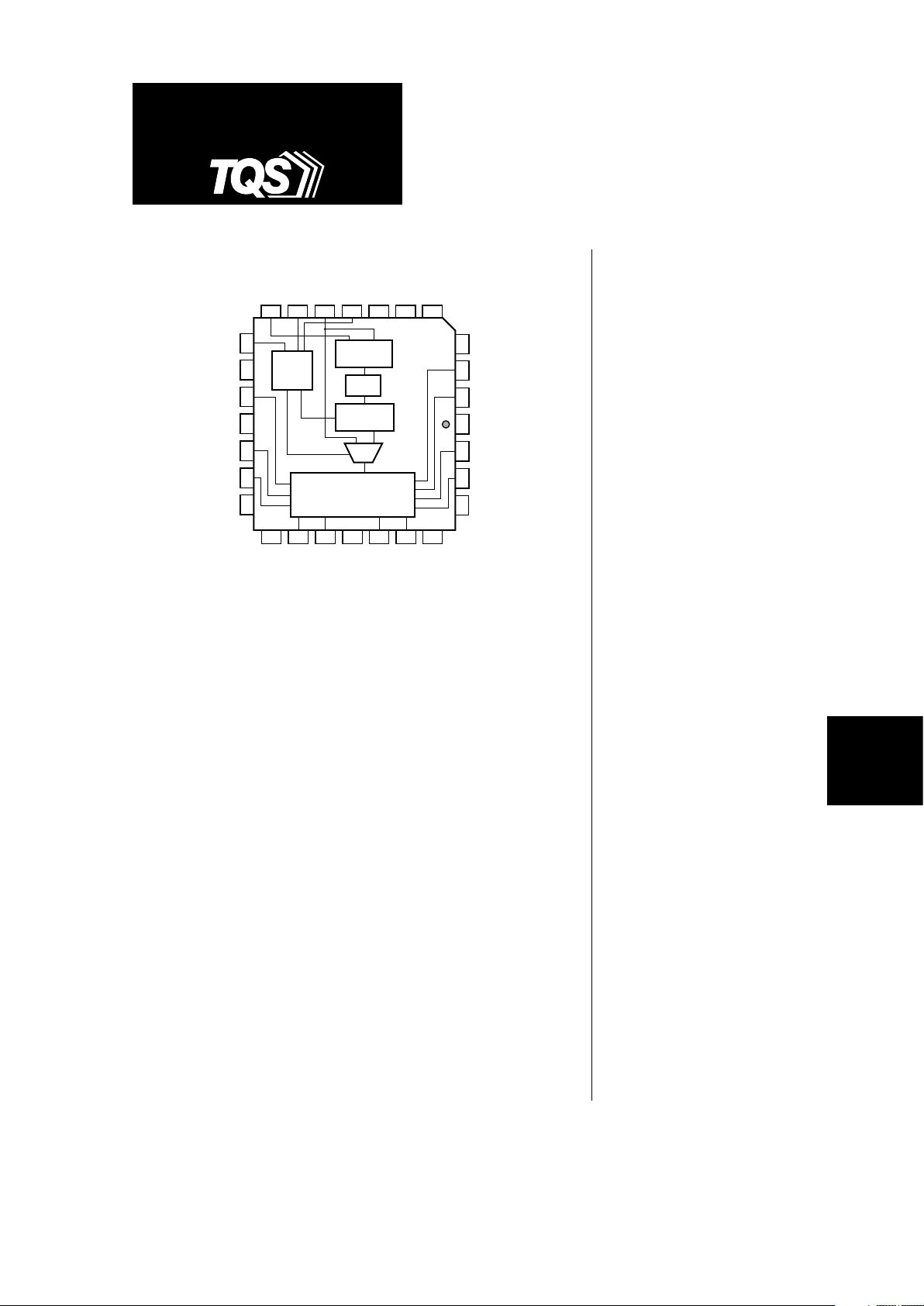
Figure 1. Block Diagram
TriQuint’s GA1086 operates from 30 MHz to 67 MHz. This TTL-level clock
buffer chip supports the tight timing requirements of high-performance
microprocessors, with near zero input-to-output delay and very low pin-topin skew. The device offers 10 usable outputs synchronized in phase and
frequency to a periodic clock input signal. One of the ten outputs is a onehalf clock output (CLK ÷ 2). With split termination, the GA1086 can be
used to drive up to nineteen 15 pF loads, as shown in Figure 10.
The tight control over phase and frequency of the output clocks is achieved
with a 400 MHz internal Phase-Locked Loop (PLL). By feeding back one of
the output clocks to FBIN, the on-chip PLL continuously maintains
synchronization between the input clock (CLK) and all ten outputs. Any
drift or gradual variation in the system clock is matched and tracked at the
ten outputs. The GA1086 output buffers are symmetric, each sourcing and
sinking up to 30 mA of drive current. For diagnostic purposes, the device
has a test mode which is used to test the device and associated logic by
single-stepping through the control logic.
The GA1086 is fabricated using TriQuint’s One-Up™ gallium arsenide
technology to achieve precise timing control and to guarantee 100% TTL
compatibility. The output frequency makes this device ideal for clock
generation and distribution in a wide range of high-performance
microprocessor-based systems. Many other CISC- and RISC-based
systems will also benefit from its tight control of skew and delay.
Precision
Output
Buffers
MUX
Divide
Logic
VCO
Phase
Detector
Control
Logic
VDD
Q9
Q8
GND
Q7
Q6
VDD
S2
VDD
Q/2
GND
FBOUT
Q1
VDD
FBIN S1 CLK S0 NC NC GND
GND Q2 Q3 VDD Q4 Q5 GND
1
2
14
13
12
4
3
22212019
18
17
16
15
27
28
252423
26
11 10
9
8765
Features
•
Operates from 30 MHz to 67MHz
•
Pin-to-pin output skew of
250 ps (max)
•
Period-to-period jitter:
75 ps (typ)
•
Near-zero propagation delay:
–350 ps
±
500 ps or
–350 ps
±
1000 ps
•
10 symmetric, TTL-compatible
outputs with 30 mA drive and
rise and fall times of 1.4 ns(max)
•
28-pin J-lead surface-mount
package
•
Special test mode
•
Meets or exceeds Pentium
™
processor timing requirements
•
Typical applications include
low-skew clock distribution for:
•
RISC- or CISC-based systems
•
Multi-processor systems
•
High-speed backplanes

GA1086
For additional information and latest specifications, see our website: www.triquint.com
2
control bit settings, divide mode and VCO range.
FBOUT is fed back to FBIN and has the same frequency
as the Qn outputs.
The GA1086 has a test mode that allows for single
stepping of the clock input for testing purposes. With
S2 HIGH, S1 LOW and S0 HIGH, the signal at the CLK
input goes directly to the outputs, bypassing the PLL
circuitry.
The maximum rise and fall time at the output pins is 1.4
ns. All outputs of the GA1086 are TTL-compatible with 30
mA symmetric drive and a minimum V
OH
of 2.4 V.
The GA1086-MC500 and GA1086-MC1000 are identical
except for the propagation delay specification (see AC
Characteristics table).
Breaking the Feedback Loop
There is no requirement that the external feedback
connection be a direct hardwire from an output pin to
the FBIN pin. As long as the signal at FBIN is derived
directly from the FBOUT pin and maintains its
frequency, additional delays can be accommodated.
The internal phase-locked loop will adjust the output
clocks on the GA1086 to ensure zero phase delay
between the FBIN and CLK signals.
Note: the signal at FBIN must be continuous, i.e. not a gated or
conditional signal.
Functional Description
The GA1086 generates 10 outputs (Q1 – Q9 and
FBOUT) which have the same frequency and zero phase
delay relative to the reference clock input. In addition,
there is one output (Q/2) that has
1
/2 the frequency of
the reference clock. The GA1086 maintains frequency
and zero phase delay using a Phase Detector to
compare the output clock with the reference clock
input. Phase deviations between the output clock and
reference clock are continuously corrected by the PLL.
Figure 1 shows a block diagram of the PLL, which
consists of a Phase Detector, Voltage Controlled
Oscillator (VCO), Divide Logic, Mux and Control Logic.
The Phase Detector monitors the phase difference
between FBIN which is connected to FBOUT, and the
reference clock (CLK). The Phase Detector adjusts the
VCO such that FBIN aligns with CLK. The VCO has an
operating range of 360 MHz to 402 MHz. The output
clocks (Qn, FBOUT, and Q/2) are generated by dividing
the VCO output.
The desired operating frequency determines the proper
divide mode. There are 4 divide modes; ÷12, ÷10, ÷8
and ÷6. In each mode, the GA1086 operates across the
frequency range listed in the Divide Mode Selection
Table. The operating frequency is equivalent to the VCO
frequency divided by the mode number.
Table 1 shows the input clock frequency (CLK), output
clock frequency (Qn),
1
/2 output clock frequency (Q/2),
Table 1. Divide Mode Selection Table
Control Divide
CLK Qn Q/2 S2 S1 S0 Mode
30 – 33 MHz 30 – 33 MHz 15 – 16.5 MHz 1 1 1 ÷12
36 – 40 MHz 36 – 40 MHz 18 – 20 MHz 1 1 0 ÷10
45 – 50 MHz 45 – 50 MHz 22.5 – 25 MHz 1 0 0 ÷8
60 – 67 MHz 60 – 67 MHz 30 – 33.5 MHz 0 1 1 ÷6
TSTCLK TSTCLK TSTCLK/2 1 0 1 —
GA1086
SYSTEM TIMING
PRODUCTS
3
For additional information and latest specifications, see our website: www.triquint.com
Power-Up/Reset Synchronization
The GA1086 utilizes on-chip phase-locked loop (PLL)
technology to maintain synchronization between inputs
and outputs. Whenever the device is powered up, or
the system clock (CLK) is reset, the phase-locked loop
requires a synchronization time (t
SYNC
) before lock is
achieved. The maximum time required for
synchronization is 500 ms.
Typical Applications
The GA1086 is designed to satisfy a wide range of
system clocking requirements. Following are two of the
most common clocking bottlenecks which can be
solved using the GA1086.
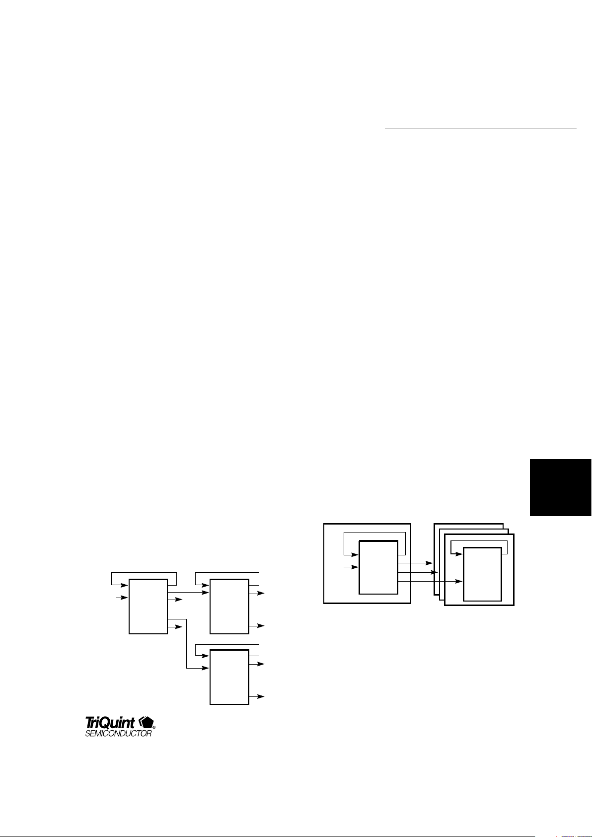
1) Low-Skew Clock Distribution / Clock Trees
The most basic bottleneck to clocking high-performance
systems is generating multiple copies of a system clock,
while maintaining low skew throughout the system.
• The GA1086 guarantees low skew among all clocks
in the system by controlling both the input-tooutput delay and the skew among all outputs. In
Figure 2, the worst-case skew from Output 1 to
Output n, with reference to the system clock, is
Figure 2. Low-Skew Clock Distribution
Figure 3. Board-to-Board Synchronization
GA1086
(1)
GA1086
(2)
GA1086
(n)
SYSTEM
CLOCK
•
•
•
•
•
•
•
•
•
Q1
Q9Q/2
OUTPUT 1
OUTPUT n
Q1
SYS
CLK
GA1000
GA1086
HOST TARGETS
t
–t
–2t
GA1110E
obtained by summing the various skews. The skew
between the outputs of the GA1086 (1) which drive
the GA1086 (2) and the GA1086 (n) is summed
with the propagation delay of the GA1086 (2 or n),
the skew between the outputs of the GA1086 (2),
and the skew between the outputs of the GA1086
(n). This results in a total skew of 1.75 ns (250 ps +
1000 ps + 250 ps + 250 ps).
2) Board-to-Board Synchronization
Many computing systems today consist of multiple
boards designed to run synchronously. The skew
associated with routing clocks across a backplane
presents a major hurdle to maximizing system
performance.
• The edge placement feature of TriQuint's
configurable custom clock generator (GA1110E)
operating at 33 MHz, coupled with the tightly
controlled input/output delay of the GA1086,
ensures all boards in the system are running
synchronously.
GA1086
For additional information and latest specifications, see our website: www.triquint.com
4
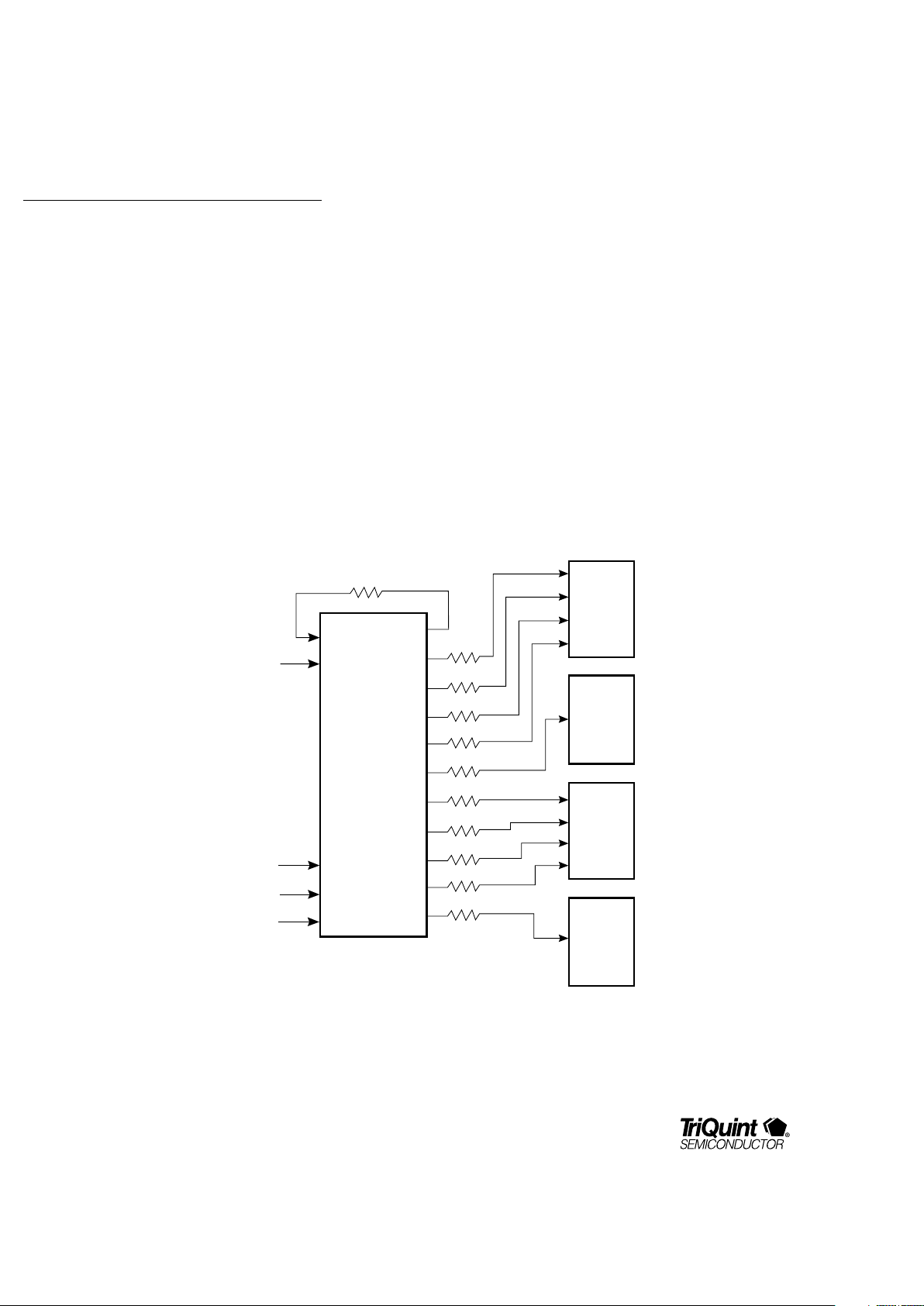
Multi-Processor Systems
The GA1086 can be effectively used to distribute clocks
in RISC- or CISC-processor-based systems. Its 10
outputs support both single- and multi-processor
systems. Following are three representative
configurations which show how the 10 outputs can be
used to synchronize the operation of CPU cache and
memory banks operating at different speeds.
CPU 1
CACHE
MEMORY
CONTROL
LOGIC
(66 MHZ)
SLOW
MEMORY
CONTROL
LOGIC
(33 MHZ)
CPU 2
CACHE
SYSTEM
CLOCK
GA1086
R
R
R
R
R
FBOUT
Q1
Q2
Q3
Q4
Q5
Q6
Q7
Q8
Q9
Q/2
R
R
R
R
R
R
FBIN
CLK
S2
S1
S0
LOW
HIGH
HIGH
Figure 4. Clocking a Dual-CPU System
Figure 4 depicts a 2-CPU system in which the
processors and associated peripherals are operating at
66 MHz. Each of the nine outputs operating at 66 MHz
are fully utilized to drive the appropriate CPU, cache,
and memory control logic. The 33 MHz output is used
to synchronize the operation of the slower memory
bank to the rest of the system.
 Loading...