

TriQuint Semiconductor Inc ETF-8103 Datasheet
T R I Q U I N T S E M I C O N D U C T O R , I N C .
TELECOM
PRODUCTS
1
For additional information and latest specifications, see our website: www.triquint.com
The TQ8103 is a monolithic clock and data recovery (CDR) IC that receives
NRZ data, extracts the high-speed clock, and presents the separated data
and clock as its outputs. This device is designed specifically for SONET
OC-12 and SDH STM-4 applications at 622 Mb/s.
Its on-chip phase-locked loop (PLL) generates a stable 622.08 Mb/s
reference based upon an external 38.88 MHz TTL reference. The PLL is
based on a VCO constructed from integrated reactive components, which
form a low-jitter, high-Q differential tank circuit. Both frequency- and
phase-detect circuits reliably acquire and hold lock in worst-case SONET
jitter conditions and scrambling patterns. The lock-detect circuitry signals
when the CDR acquires frequency lock.
Typical SONET/SDH system applications for the TQ8103 include:
• Transmission system transport cards
• Switch and cross-connect line cards
• ATM physical layer interfaces
• Test equipment
• Add/drop multiplexers
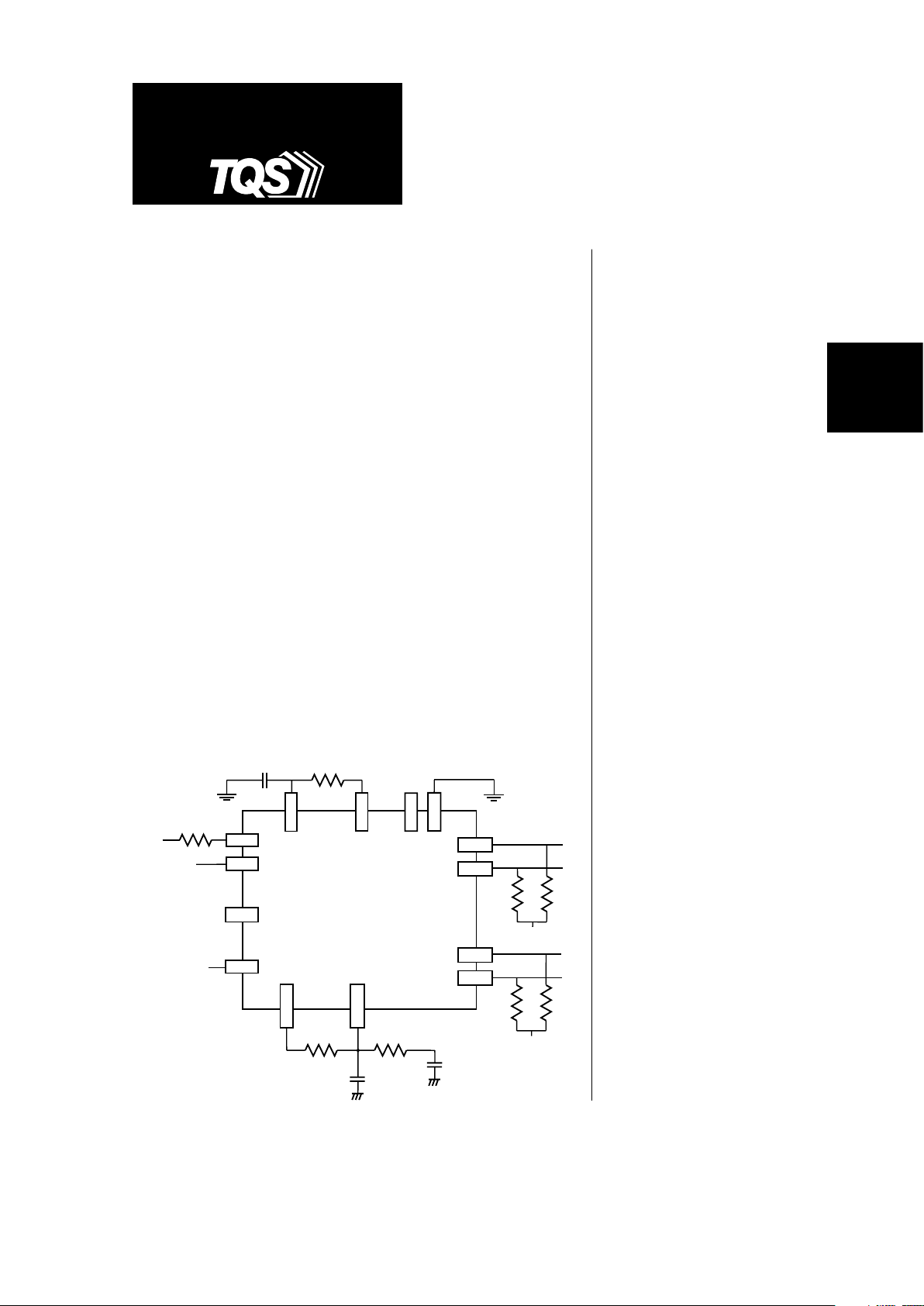
Figure 1. Typical Application
TQ8103
622 Mb/s Clock
& Data Recovery
Features
• Single-chip CDR circuit for
622 Mb/s data
• Exceeds Bellcore and ITU jitter
tolerance maps
• Single-ended ECL input has loopthrough path for external 50 ohm
termination to minimize stubs
and reflections
• Clock and data outputs are
differential ECL
• Provides complete high-speed
OC-12/STM-4 solution when
used with TQ8101 or TQ8105
Mux/Demux/Framer/PLL
• External loop filter requires
simple passive network
•
Maintains clock in absence of data
• 28-pin leaded chip carrier
• Can be used with a high-speed
external clock
OUCHP
LOCK
CKREF
V
CTL
D
OUTP
SINI
SINO
XTCKI
SELCK
SEL
V
REF
CK
OUTP
CK
OUTN
V
TT
ECL data in
(single-ended)
38.88-MHz TTL
clock oscillator
20K Ω 62 Ω
1 mF
50 Ω
V
TT
10K Ω
1000 pF
V
TT
D
OUTN
50 Ω
50 Ω
1000 pF
TQ8103
2
For additional information and latest specifications, see our website: www.triquint.com
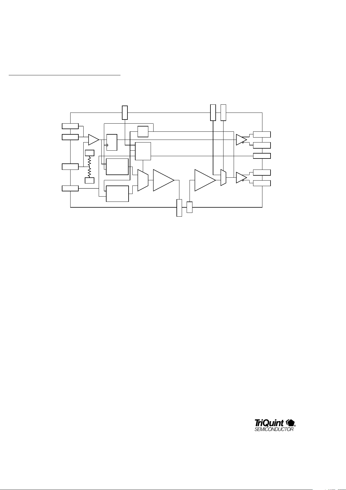
Figure 2. TQ8103 Block Diagram
Functional Description
The TQ8103 CDR integrates separate detectors for
acquiring frequency lock and maintaining precise phase
lock. When the CDR is locked onto an incoming NRZ
data stream, its phase-detect circuitry compares the
phase of the incoming NRZ data and the phase of the
generated 622.08 MHz clock. When they differ, the
resulting error signal nulls the phase difference and
puts the generated 622.08 MHz clock back in phase
with the incoming data. In this mode, the LOCK output
is high.
The phase-detect circuit operates only when the
incoming NRZ data transitions between states. SONET
and SDH employ scrambling, which provides an
average transition density of 50 percent; however, some
data patterns can generate legitimate scrambled signals
with a significant number of consecutive ones or zeros.
The TQ8103 maintains lock over bit sequences of over
100 consecutive zeros or ones.
When the input data is lost or too many bit times occur
without a transition, the PLL (which generates the
622.08 MHz clock) eventually drifts. The lock-detect
circuit constantly compares the generated 622.08 MHz
clock (divided by 16) and the external 38.88 MHz
reference. When the PLL drifts more than 2000 PPM
from the reference, the LOCK output goes low.
The SEL input selects between the phase-detect and
frequency-detect circuits. When the PLL drifts out of
lock, taking SEL low reverses the drift by switching in
the frequency-detect circuit. Connecting the LOCK
output directly to the SEL input should ensure that
frequency lock is maintained in the absence of data.
It is recommended, however, that a low-pass filter be
added between LOCK and SEL to allow for orderly
transitions between these circuits. Once the PLL
frequency is within 500 PPM of the reference, the LOCK
output returns high. As the SEL input goes high, the
phase-detect circuit again maintains lock to the
incoming NRZ data.
The TQ8103 can also be used as a standalone 622.08 MHz
frequency reference. When SEL is held low, the PLL
utilizes only the frequency-detect circuit. The PLL locks
onto the external 38.88 MHz reference to generate the
desired 622.08 MHz output.
Frequency
Detect
Charge
Pump
VCO
CKREF
OUCHP
V
CTL
D
OUTP
LOCK
SINI
SINO
XTCKI
SELCK
Phase
Detect
D
Q
+16
Lock
Detect
Mux
SEL
V
REF
V
EE
V
DD
D
OUTN
CK
OUTP
CK
OUTN
TQ8103
TELECOM
PRODUCTS
For additional information and latest specifications, see our website: www.triquint.com
3
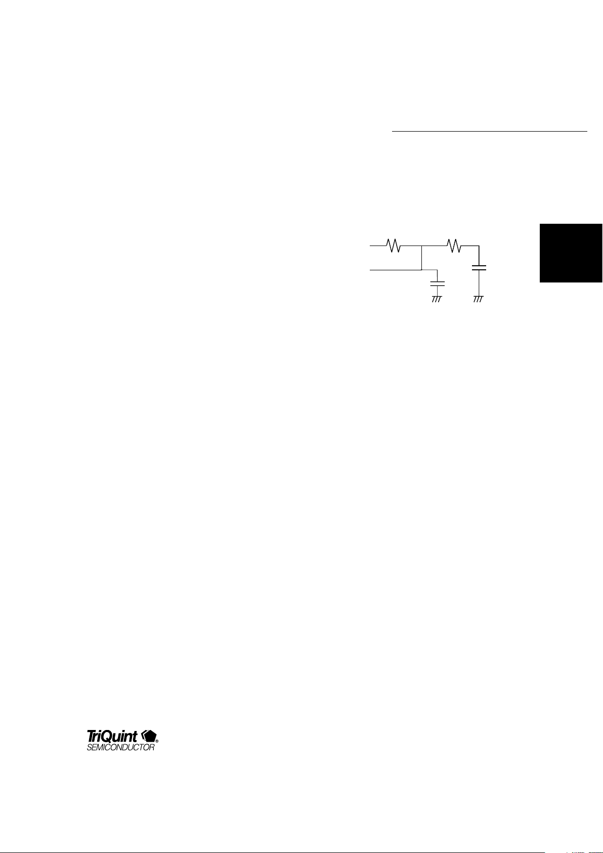
Application Information
Loop Filter Design
The TQ8103 requires an external loop filter. Care should
be taken in the implementation of the filter. Good highfrequency design techniques should be used, with the
loop filter being connected into the analog ground. The
analog supply should be well filtered.
Data Input Considerations
The serial data input line is a high-frequency ECL signal,
and should be kept in a 50 ohm controlled impedance
environment. Reflections on the serial input are
minimized through the use of a separate loopback
termination pin, SINO. A 50 ohm chip resistor between
SINO and V
TT
minimizes stub length for the best signal
quality. Another physical design consideration is to
place the TQ8103 and its companion high-speed ICs as
close as possible to the optics while observing good
analog design practice on supply filtering and
grounding.
External Frequency Reference
The externally supplied 38.88 MHz CKREF input needs
to have low jitter with fast rise and fall times. Typical
applications will use a telecom crystal oscillator such as
the Connor-Winfield S14R6-38.88. SONET requires frequency sources to be accurate to ±20␣ ppm over temperature, voltage, and aging. The CKREF input is a refer
ence
frequency for initial frequency lock and for the lock-detect
circuit, so it can tolerate accuracies of up to ±100␣ ppm.
Jitter Tolerance
Jitter tolerance describes the ability of the CDR circuit
to track timing variations (jitter) in the received signal.
The Bellcore and ITU specifications allow the received
optical signal to contain jitter. The amount of jitter that
must be tolerated is a function of the frequency content
of the jitter. The CDR must tolerate many unit intervals
(bit times) of low-frequency jitter, but is not asked to
tolerate large amounts of jitter at higher frequency. The
performance shown in the “Typical Performance Data”
section shows that the TQ8103 offers a wide margin
over the specification limits.
Jitter tolerance is a system-level issue that is directly
affected by the quality of the optics, the quality of the
layout (and decoupling), and the specific
implementation of the loop filter. The recommended
loop filter, described above, has been chosen to provide
a robust margin on jitter tolerance.
Figure 3. External Loop Filter
OUCHP
V
CTL
1 mF
62 Ω
20 KΩ
1000 pF
 Loading...