

TriQuint TQP7M9102 Schematic [ru]
Datasheet: Rev. K 01-26-16
- 1 of 26 -
Disclaimer: Subject to change without notice
© 2016 TriQuint Semiconductor, Inc
www.triquint.com / www.qorvo.com
Applications
Repeaters
Mobile Infrastructure
CDMA / WCDMA / LTE
General Purpose Wireless
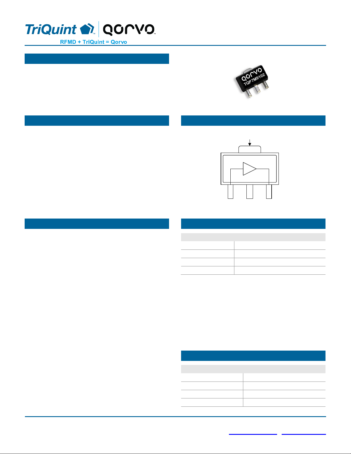
3 Pin SOT-89 Package
Product Features
400-4000 MHz
+27.5 dBm P1dB
+44 dBm Output IP3
17.8 dB Gain at 2140 MHz
+5 V Single Supply, 135 mA Current
Internal RF overdrive protection
Internal DC overvoltage protection
On chip ESD protection
SOT-89 Package
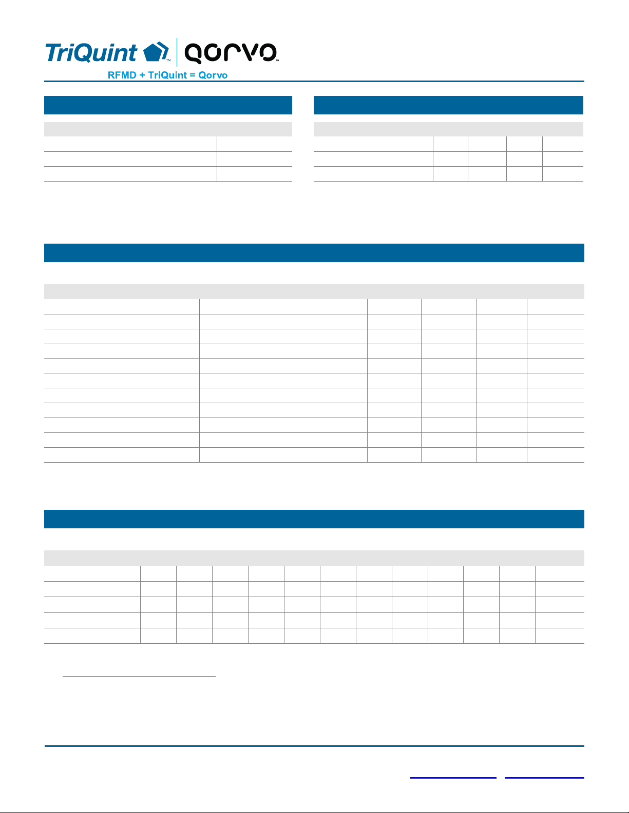
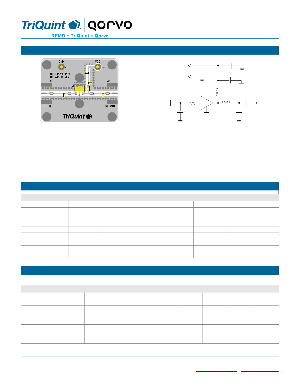
Functional Block Diagram
General Description
The TQP7M9102 is a high linearity driver amplifier in a
low-cost, RoHS compliant, surface mount package. This
InGaP/GaAs HBT delivers high performance across a
broad range of frequencies with +44 dBm OIP3 and +27.5
dBm P1dB while only consuming 135 mA quiescent
current. All devices are 100% RF and DC tested.
The TQP7M9102 incorporates on-chip features that
differentiate it from other products in the market. The
amplifier integrates an on-chip DC over-voltage and RF
over-drive protection. This protects the amplifier from
electrical DC voltage surges and high input RF input
power levels that may occur in a system. On-chip ESD
protection allows the amplifier to have a very robust Class
2 HBM ESD rating.
The TQP7M9102 is targeted for use as a driver amplifier
in wireless infrastructure where high linearity, medium
power, and high efficiency are required. The device an
excellent candidate for transceiver line cards in current
and next generation multi-carrier 3G / 4G base stations.
Pin Configuration
Pin No.
Label
1
RF IN
2
GND
3
RF OUT / V
CC
Backside Paddle
GND
Ordering Information
Part No.
Description
TQP7M9102
0.5 W High Linearity Amplifier
TQP7M9102−PCB900
869−960 MHz Evaluation Board
TQP7M9102−PCB2140
2.11–2.17 GHz Evaluation Board
TQP7M9102−PCB2600
2.5–2.7 GHz Evaluation Board
Standard T/R size = 1000 pieces on a 7” reel
RF IN GND RF OUT / V
CC
1 2 3
Backside Paddle - GND
TQP7M9102
½ W High Linearity Amplifier
Datasheet: Rev. K 01-26-16
- 2 of 26 -
Disclaimer: Subject to change without notice
© 2016 TriQuint Semiconductor, Inc
www.triquint.com / www.qorvo.com
Recommended Operating Conditions
Parameter
Min
Typ
Max
Units
Device Voltage (V
CC)
+4.75
+5
+5.25
V
T
CASE
-40 +105
°C
Tj for >106 hours MTTF
+170
°C
Electrical specifications are measured at specified test
conditions. Specifications are not guaranteed over all
recommended operating conditions.
Absolute Maximum Ratings
Parameter
Rating
Storage Temperature
−65 to +150°C
RF Input Power, CW, 50Ω, T=25°C
+27 dBm
Device Voltage (VCC)
+8 V
Operation of this device outside the parameter ranges
given above may cause permanent damage.
Electrical Specifications
Test conditions unless otherwise noted: VCC=+5V, Temp.=+25 °C, matched 2140 MHz reference circuit
Parameter
Conditions
Min
Typ
Max
Units
Operational Frequency Range
400
4000
MHz
Test Frequency
2140
MHz
Gain 15.5
17.8 dB
Input Return Loss
12 dB
Output Return Loss
10 dB
Output P1dB
+26.4
+27.5
dBm
Output IP3
Pout = +9 dBm/tone, ∆f = 1 MHz
+41
+43.8
dBm
WCDMA Channel Power
(1)
−50 dBc ACLR
+18.5
dBm
Noise Figure
3.9 dB
Quiescent Current, ICQ
See Note 1
115
137
155
mA
Thermal Resistance, θ
jc
Junction to case
50
°C/W
Notes:
1. ACLR test set-up: 3GPP WCDMA, TM1+64 DPCH, +5 MHz offset, PAR = 10.2 dB at 0.01% Probability
Performance Summary Table
Test conditions unless otherwise noted: VCC =+5V, Temp.= +25 °C, band specific matching networks
(1)
Frequency
768
869
960
1540
1840
1960
2140
2140
2350
2600
3500
MHz
Gain
20.9
21.8
21.7
20.2
20.0
18.4
15.5
17.8
16.0
14.5
14.5
dB
Input Return Loss
9
10
17
15
17
13 8 12
17
14.5
17
dB
Output Return Loss
8
12
9
6
7.5
7 8 11
8 8 11
dB
Output P1dB
+28.4
+27.3
+27.4
+28.2
+27.5
+27.0
+30.7
+27.6
+27.2
+28.0
+26.2
dBm
Output IP3
+44
+43
+44
+51
+42
+46
+38
+44
+44
+44
+45
dBm
Notes:
1. Reference designs for the various frequencies are either included on this datasheet or may be obtained by contacting
sjcapplications.engineering@tqs.com.
TQP7M9102
½ W High Linearity Amplifier
Datasheet: Rev. K 01-26-16
- 3 of 26 -
Disclaimer: Subject to change without notice
© 2016 TriQuint Semiconductor, Inc
www.triquint.com / www.qorvo.com
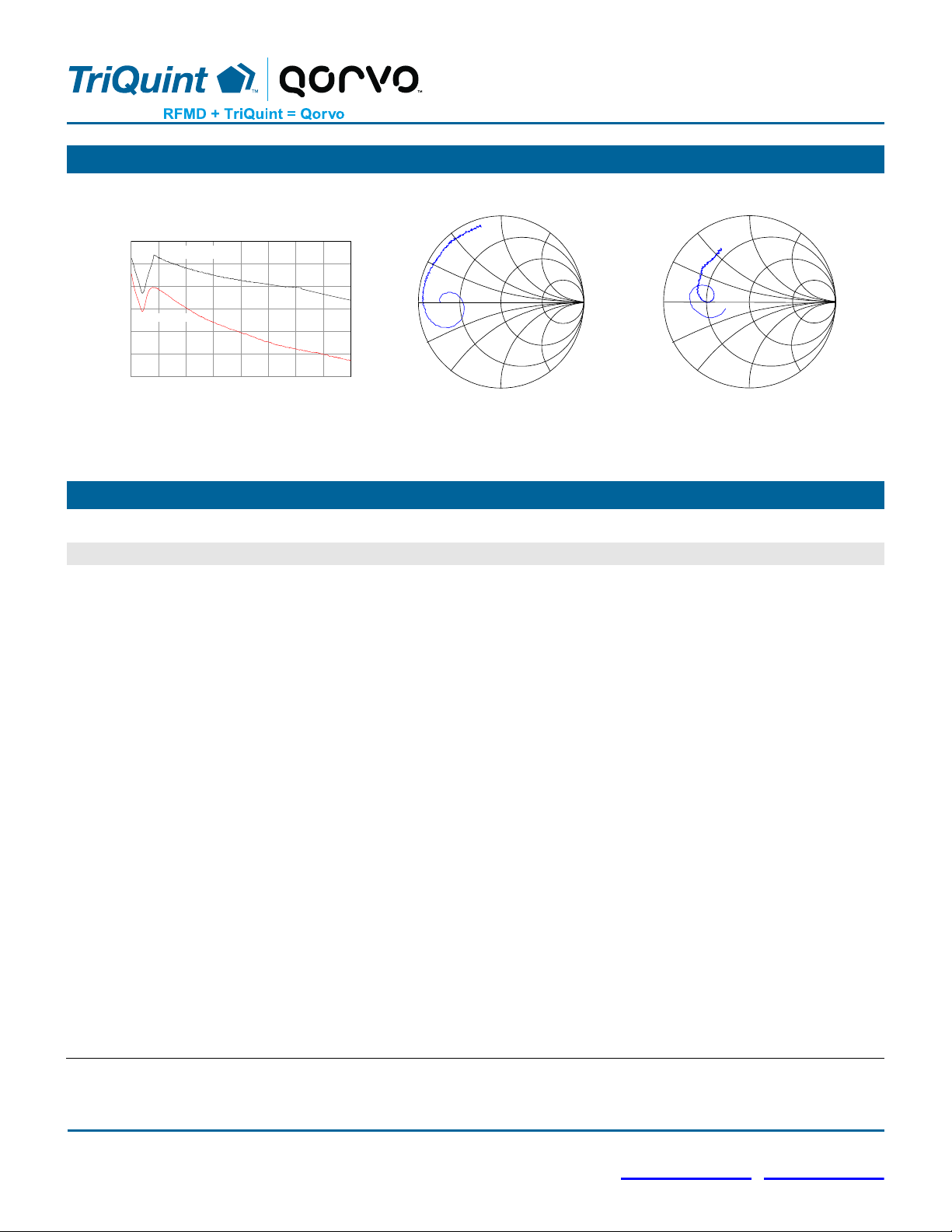
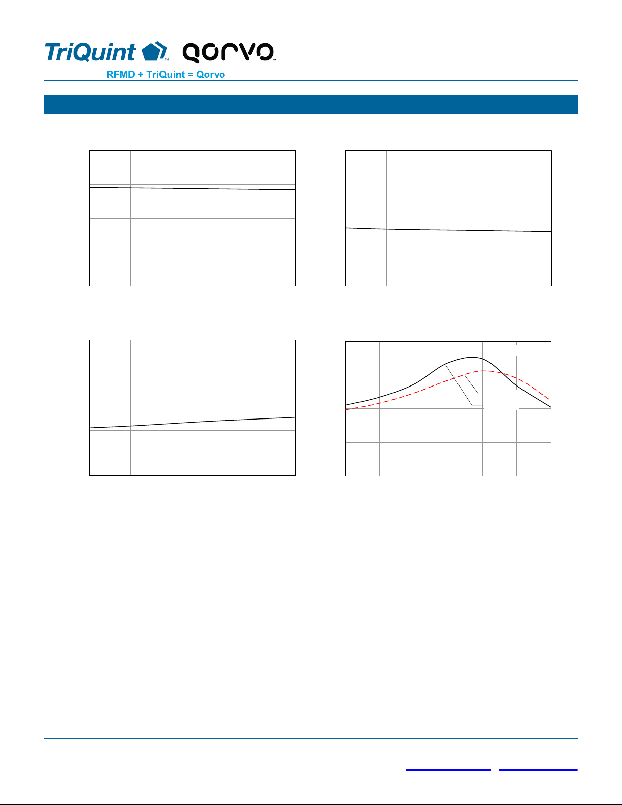
Device Characterization Data
Note: The gain for the unmatched device in a 50 ohm system is shown as the black trace labeled "Gain (S21)". In a circuit tuned for a particular
frequency, it is expected that actual gain will be higher, up to the maximum stable gain. The maximum stable gain is shown as the red trace
[Gmax]. The impedance Smith chart plots are shown from 0.01 to 4 GHz.
S-Parameters
Test Conditions: VCC=+5 V, ICQ=135 mA (typ.), Temp.=+25 °C, unmatched 50 Ohm system, reference plane at device leads
Freq (MHz)
S11 (dB)
S11 (ang)
S21 (dB)
S21 (ang)
S12 (dB)
S12 (ang)
S22 (dB)
S22 (ang)
50
-2.55
176.64
20.38
156.15
-35.04
-9.37
-5.88
-159.98
100
-2.91
172.21
18.15
151.53
-35.97
-20.12
-4.45
-167.94
200
-5.79
172.18
14.52
160.74
-41.94
-60.14
-3.20
177.62
400
-1.41
-163.37
19.80
154.97
-34.61
49.55
-7.14
165.58
600
-0.52
179.77
18.56
125.67
-33.11
19.10
-6.55
178.58
800
-0.45
171.80
16.85
108.86
-32.96
8.46
-5.41
178.08
1000
-0.49
165.43
15.28
95.36
-32.92
-1.08
-4.76
174.13
1200
-0.60
160.30
13.79
85.52
-33.15
-4.65
-4.38
171.06
1400
-0.60
157.51
12.55
77.70
-33.23
-9.05
-4.24
167.58
1600
-0.67
152.76
11.49
69.57
-33.03
-15.12
-4.15
163.37
1800
-0.74
148.28
10.53
62.39
-32.96
-19.02
-4.00
159.18
2000
-0.72
143.55
9.75
54.69
-33.03
-20.90
-3.89
155.31
2200
-0.78
139.03
8.88
48.56
-32.96
-25.51
-3.77
150.66
2400
-0.71
135.24
7.99
42.25
-32.88
-27.98
-3.40
146.69
2600
-0.74
131.98
7.23
36.47
-33.43
-30.45
-3.38
144.96
2800
-0.75
128.79
6.58
31.19
-33.15
-33.43
-3.44
142.02
3000
-0.80
126.32
6.09
26.41
-33.23
-36.48
-3.50
139.73
3200
-0.75
122.75
5.69
20.73
-33.43
-37.86
-3.39
137.14
3400
-0.81
118.06
5.30
14.38
-33.39
-44.57
-3.48
130.99
3600
-0.82
113.62
4.59
7.77
-33.03
-43.44
-3.34
124.40
3800
-0.71
108.88
4.07
1.73
-32.92
-50.92
-3.04
120.16
4000
-0.68
105.86
3.64
-2.85
-33.15
-54.00
-2.92
118.44
0
5
10
15
20
25
30
0 0.5 1 1.5 2 2.5 3 3.5 4
Gain (dB)
Frequency (GHz)
Gain and Maximum Stable Gain
Gain (Max)
Gain (S21)
-1
-0.8
-0.6
-0.4
-0.2
0
0.2
0.4
0.6
0.8
1
-1 -0.75-0.5-0.25 0 0.250.50.75 1
Input Smith Chart
0.01 GHz
4 GHz
Output Smith Chart
0.01 GHz
4 GHz
TQP7M9102
½ W High Linearity Amplifier
Datasheet: Rev. K 01-26-16
- 4 of 26 -
Disclaimer: Subject to change without notice
© 2016 TriQuint Semiconductor, Inc
www.triquint.com / www.qorvo.com
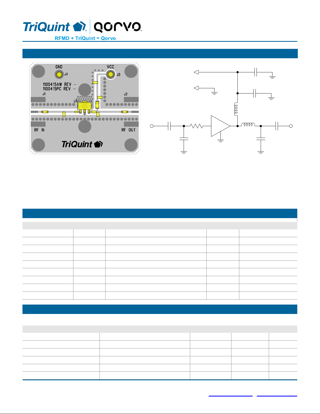
746 – 768 MHz Reference Design
Notes:
1. See Evaluation Board PCB Information for material and stack up.
2. The recommended component values are dependent upon the frequency of operation.
3. All components are of 0603 size unless stated on the schematic.
4. Critical component placement locations:
Distance from U1 Pin Pad 1 (left edge) to R1 (right edge): 0 mils
Distance from U1 Pin Pad 1 (left edge) to C6 (right edge): 60 mils
Distance from U1 Pin Pad 1 (left edge) to C5 (right edge): 230 mils
Distance from U1 Pin Pad 3 (right edge) to L2 (left edge): 0 mils
Bill of Material 746 – 768 MHz Reference Design
Reference Des.
Value
Description
Manuf.
Part Number
n/a
n/a
Printed Circuit Board
Qorvo
U1
n/a
½ W High Linearity Amplifier
Qorvo
TQP7M9102
C1 , C2 , C3
100 pF
CAP, 0603, +/-5%. 100V NPO/COG
various
C5
12 pF
CAP, 0603, +/-2%. 50V. NPO/COG
various
C6
4.7 pF
CAP, 0603, +/-0.1PF. 100V. NPO/COG
various
C4
1.0 uF
CAP, 0603, 10%, X5R , 10V
various
L1
33 nH
IND, 0805, 5%, Ceramic
Coilcraft
0805CS-331XJL
L2
4.7 nH
IND, 0603, +/-0.3. >5600MHZ
Toko
LL1608-FSL4N7S
C4
1.0 uF
Cap., Chip, 10%, 10V, X5R
various
Typical Performance 746 – 768 MHz Reference Design
Test conditions unless otherwise noted: VCC=+5 V, ICQ=137 mA (typ.), Temp.=+25 °C
Parameter
Conditions
Typical Value
Units
Frequency
746
768
MHz
Gain 20.9
20.9
dB
Input Return Loss
8
9
dB
Output Return Loss
10
8
dB
Output P1dB
+28.2
+28.4
dBm
Output IP3
Pout= +18 dBm/tone, f= 1 MHz
+47
+44
dBm
J4
J3
U1
L1
C2
C3
C4
C1
R1
C5
L2
C6
U1
TQP7M9102
J4 GND
J3 Vcc
1
2,4
3
J1
RF
Input
J2
RF
Output
L1
0805
33 nH
C1
100 pF
C4
1.0 uF
C3
100 pF
R1
0402
3.0
C6
4.7 pF
C2
100 pF
L2
4.7 nH
C5
12 pF
TQP7M9102
½ W High Linearity Amplifier
Datasheet: Rev. K 01-26-16
- 5 of 26 -
Disclaimer: Subject to change without notice
© 2016 TriQuint Semiconductor, Inc
www.triquint.com / www.qorvo.com
Performance Plots 746 – 768 MHz Reference Design
18
19
20
21
22
745 750 755 760 765 770
Gain (dB)
Frequency (MHz)
Gain vs. Frequency
Temp.=+25°C
-15
-10
-5
0
745 750 755 760 765 770
|S11| (dB)
Frequency (MHz)
Input Return Loss vs. Frequency
Temp.=+25°C
-15
-10
-5
0
745 750 755 760 765 770
|S22| (dB)
Frequency (MHz)
Output Return Loss vs. Frequency
Temp.=+25°C
30
35
40
45
50
15 16 17 18 19 20 21
OIP3 (dBm)
Pout/Tone (dBm)
OIP3 vs. Pout/tone
Temp.=+25°C
768 MHz
746 MHz
TQP7M9102
½ W High Linearity Amplifier
Datasheet: Rev. K 01-26-16
- 6 of 26 -
Disclaimer: Subject to change without notice
© 2016 TriQuint Semiconductor, Inc
www.triquint.com / www.qorvo.com
869 – 894 MHz Evaluation Board (TQP7M9102−PCB900)
Notes:
1. See Evaluation Board PCB Information for material and stack up.
2. Components shown on the silkscreen but not on the schematic are not used.
3. The recommended component values are dependent upon the frequency of operation.
4. All components are of 0603 size unless stated on the schematic.
5. Critical component placement locations:
Distance from U1 Pin 1 (left edge) to R1 (right edge): 90 mils (4.3 deg. at 920 MHz)
Distance from R1 (left edge) to C5 (right edge): 70 mils (3.3 deg. at 920 MHz)
Distance from U1 Pin 3 (right edge) to L2 (left edge): 120 mils (5.7 deg. at 920 MHz)
Distance from U1 Pin 3 (right edge) to C6 (left edge): 370 mils (17.6 deg. at 920 MHz)
Bill of Material TQP7M9102−PCB900
Reference Des.
Value
Description
Manuf.
Part Number
n/a
n/a
Printed Circuit Board
Qorvo
U1
n/a
TQP7M9102 Amplifier, SOT-89 pkg.
Qorvo
TQP7M9102
R1
1.8 Ω
Resistor, Chip, 0603, 5%, 1/16W
various
L2
3.3 nH
Inductor, 0603, +/-0.3 nH
Toko
LL1608-FSL3N3S
L1
33 nH
Inductor, 0805, 5%, Coilcraft CS Series
Coilcraft
0805CS-330XJLB
C5
8.2 pF
Cap., Chip, 0603, +/-0.1pF. 200V.
AVX
06032U8R2BAT2A
C6
3.3 pF
Cap., Chip, 0603, +/-0.1pF. 200V.
AVX
06032U3R3BAT2A
C1, C2, C3
100 pF
Cap., Chip, 5%, 50V, NPO/COG
various
C4
1.0 uF
Cap., Chip, 10%, 10V, X5R
various
Typical Performance TQP7M9102−PCB900
Test conditions unless otherwise noted: VCC=+5V, ICQ=137 mA (typ.), Temp.=+25 °C
Parameter
Conditions
Typical Value
Units
Frequency
869
920
960
MHz
Gain 21.8
21.9
21.7
dB
Input Return Loss
10
16
17
dB
Output Return Loss
12
10 9 dB
Output P1dB
+27.3
+27.4
+27.4
dBm
OIP3
Pout= +19 dBm/tone, Δf=1 MHz
+42.7
+43.4
+43.9
dBm
WCDMA Channel Power
(1)
−50 dBc ACLR
+18.0
+18.2
+18.1
dBm
Noise Figure
5.9
5.9
5.9
dB
Notes:
1. ACLR Test set-up: 3GPP WCDMA, TM1+64 DPCH, +5 MHz offset, PAR = 10.2 dB at 0.01% Probability
J4
J3
U1
L1
C2
C3
C4
C1
R1
C5
L2
C6
U1
TQP7M9102
J4 GND
J3 Vcc
1
2,4
3
J1
RF
Input
J2
RF
Output
L1
33 nH
0805
C1
100 pF
C4
1 uF
C3
100 pF
C2
100 pF
C5
8.2 pF
C6
3.3 pF
R1
1.8
L2
3.3 nH
TQP7M9102
½ W High Linearity Amplifier
Datasheet: Rev. K 01-26-16
- 7 of 26 -
Disclaimer: Subject to change without notice
© 2016 TriQuint Semiconductor, Inc
www.triquint.com / www.qorvo.com
Performance Plots TQP7M9102−PCB900
Test conditions unless otherwise noted: VCC=+5V, ICQ=137 mA (typ.), Temp.=+25 °C
19
20
21
22
23
24
860 880 900 920 940 960
Gain (dB)
Freq (MHz)
Gain vs. Frequency
+85°C
+25°C
−40°C
-25
-20
-15
-10
-5
0
860 880 900 920 940 960
|S11| (dB)
Freq (MHz)
Input Return Loss vs. Frequency
+85°C
+25°C
−40°C
-25
-20
-15
-10
-5
0
860 880 900 920 940 960
|S22| (dB)
Freq (MHz)
Output Return Loss vs. Frequency
+85°C
+25°C
−40°C
-65
-60
-55
-50
-45
-40
-35
12 13 14 15 16 17 18 19 20
ACLR (dBc)
Pout (dBm)
ACLR Vs. Output Power
+85°C
+25°C
−40°C
W-CDMA 3GPP Test Model 1+64 DPCH
PAR = 10.2 dB @ 0.01% Probability
3.84 MHz BW
Freq.=920 MHz
36
38
40
42
44
46
11 13 15 17 19 21
OIP3 (dBm)
Pout/Tone (dBm)
OIP3 Vs. Pout/Tone
+85°C
+25°C
−40°C
Freq.=920 MHz
1 MHz Tone Spacing
25
26
27
28
29
30
860 880 900 920 940 960
P1dB (dBm)
Frequency (MHz)
P1dB vs. Frequency
−40°C
+25°C
+85°C
-65
-60
-55
-50
-45
-40
-35
12 13 14 15 16 17 18 19 20
ACLR (dBc)
Pout (dBm)
ACLR Vs. Output Power
960 MHz
920 MHz
869 MHz
W-CDMA 3GPP Test Model 1+64 DPCH
PAR = 10.2 dB @ 0.01% Probability
3.84 MHz BW
Temp.=+25°C
30
35
40
45
50
11 13 15 17 19 21
OIP3 (dBm)
Pout/Tone (dBm)
OIP3 Vs. Pout/Tone
960 MHz
920 MHz
869 MHz
1 MHz Tone Spacing
Temp.=+25°C
19
21
23
25
27
29
-3 -1 1 3 5 7
Pout (dBm)
Pin (dBm)
Output Power vs. Input Power
−40°C
+25°C
+85°C
Freq.= 920 MHz
120
140
160
180
200
220
240
260
12 14 16 18 20 22 24 26 28
Icc (mA)
Pout (dBm)
Icc vs. Output Power
+85°C
+25°C
−40°C
Frequency = 920 MHz
TQP7M9102
½ W High Linearity Amplifier

Datasheet: Rev. K 01-26-16
- 8 of 26 -
Disclaimer: Subject to change without notice
© 2016 TriQuint Semiconductor, Inc
www.triquint.com / www.qorvo.com
700 – 1000 MHz Evaluation Board (TQP7M9102−PCB900)
Notes:
1. See Evaluation Board PCB Information for material and stack up.
2. Components shown on the silkscreen but not on the schematic are not used.
3. The recommended component values are dependent upon the frequency of operation.
4. All components are of 0603 size unless stated on the schematic.
5. Critical component placement locations:
Distance from U1 Pin 1 (left edge) to R1 (right edge): 90 mils (4.3 deg. at 920 MHz)
Distance from R1 (left edge) to C5 (right edge): 70 mils (3.3 deg. at 920 MHz)
Distance from U1 Pin 3 (right edge) to L2 (left edge): 120 mils (5.7 deg. at 920 MHz)
Distance from U1 Pin 3 (right edge) to C6 (left edge): 370 mils (17.6 deg. at 920 MHz)
Bill of Material TQP7M9102−PCB900
Reference Des.
Value
Description
Manuf.
Part Number
n/a
n/a
Printed Circuit Board
Qorvo
U1
n/a
TQP7M9102 Amplifier, SOT-89 pkg.
Qorvo
TQP7M9102
R1
1.8 Ω
Resistor, Chip, 0603, 5%, 1/16W
various
L2
3.3 nH
Inductor, 0603, ±0.3 nH
Toko
LL1608-FSL3N3S
L1
33 nH
Inductor, 0805, 5%, Coilcraft CS Series
Coilcraft
0805CS-330XJLB
C5
8.2 pF
Cap., Chip, 0603, ±0.1pF. 200V. NPO/COG
AVX
06032U8R2BAT2A
C6
3.3 pF
Cap., Chip, 0603, ±0.1pF. 200V. NPO/COG
AVX
06032U3R3BAT2A
C1, C2, C3
100 pF
Cap., Chip, 5%, 50V, NPO/COG
various
C4
1.0 uF
Cap., Chip, 10%, 10V, X5R
various
Typical Performance TQP7M9102−PCB900
Test conditions unless otherwise noted: VCC=+5V, ICQ=137 mA (typ.), Temp.=+25 °C
Parameter
Conditions
Typical Value
Units
Frequency
869
920
960
MHz
Gain 21.8
21.9
21.7
dB
Input Return Loss
10
16
17
dB
Output Return Loss
12
10 9 dB
Output P1dB
+27.3
+27.4
+27.4
dBm
OIP3
Pout= +19 dBm/tone, Δf=1 MHz
+42.7
+43.4
+43.9
dBm
WCDMA Channel Power
(1)
−50 dBc ACLR
+18.0
+18.2
+18.1
dBm
Noise Figure
5.9
5.9
5.9
dB
Notes:
1. ACLR Test set-up: 3GPP WCDMA, TM1+64 DPCH, +5 MHz offset, PAR = 10.2 dB at 0.01% Probability
J4
J3
U1
L1
C2
C3
C4
C1
R1
C5
L2
C6
U1
TQP7M9102
J4 GND
J3 Vcc
1
2,4
3
J1
RF
Input
J2
RF
Output
L1
33 nH
0805
C1
100 pF
C4
1 uF
C3
100 pF
C2
100 pF
C5
8.2 pF
C6
3.3 pF
R1
1.8
L2
3.3 nH
TQP7M9102
½ W High Linearity Amplifier

Datasheet: Rev. K 01-26-16
- 9 of 26 -
Disclaimer: Subject to change without notice
© 2016 TriQuint Semiconductor, Inc
www.triquint.com / www.qorvo.com
Performance Plots TQP7M9102−PCB900
Test conditions unless otherwise noted: VCC=+5V, ICQ=137 mA (typ.), Temp.=+25 °C
19
20
21
22
23
24
860 880 900 920 940 960
Gain (dB)
Freq (MHz)
Gain vs. Frequency
+85°C
+25°C
−40°C
-25
-20
-15
-10
-5
0
860 880 900 920 940 960
|S11| (dB)
Freq (MHz)
Input Return Loss vs. Frequency
+85°C
+25°C
−40°C
-25
-20
-15
-10
-5
0
860 880 900 920 940 960
|S22| (dB)
Freq (MHz)
Output Return Loss vs. Frequency
+85°C
+25°C
−40°C
-65
-60
-55
-50
-45
-40
-35
12 13 14 15 16 17 18 19 20
ACLR (dBc)
Pout (dBm)
ACLR Vs. Output Power
+85°C
+25°C
−40°C
W-CDMA 3GPP Test Model 1+64 DPCH
PAR = 10.2 dB @ 0.01% Probability
3.84 MHz BW
Freq.=920 MHz
36
38
40
42
44
46
11 13 15 17 19 21
OIP3 (dBm)
Pout/Tone (dBm)
OIP3 Vs. Pout/Tone
+85°C
+25°C
−40°C
Freq.=920 MHz
1 MHz Tone Spacing
25
26
27
28
29
30
860 880 900 920 940 960
P1dB (dBm)
Frequency (MHz)
P1dB vs. Frequency
−40°C
+25°C
+85°C
-65
-60
-55
-50
-45
-40
-35
12 13 14 15 16 17 18 19 20
ACLR (dBc)
Pout (dBm)
ACLR Vs. Output Power
960 MHz
920 MHz
869 MHz
W-CDMA 3GPP Test Model 1+64 DPCH
PAR = 10.2 dB @ 0.01% Probability
3.84 MHz BW
Temp.=+25°C
30
35
40
45
50
11 13 15 17 19 21
OIP3 (dBm)
Pout/Tone (dBm)
OIP3 Vs. Pout/Tone
960 MHz
920 MHz
869 MHz
1 MHz Tone Spacing
Temp.=+25°C
19
21
23
25
27
29
-3 -1 1 3 5 7
Pout (dBm)
Pin (dBm)
Output Power vs. Input Power
−40°C
+25°C
+85°C
Freq.= 920 MHz
120
140
160
180
200
220
240
260
12 14 16 18 20 22 24 26 28
Icc (mA)
Pout (dBm)
Icc vs. Output Power
+85°C
+25°C
−40°C
Frequency = 920 MHz
TQP7M9102
½ W High Linearity Amplifier
 Loading...