

TriQuint CFH 400 Technical data
查询CFH400供应商
CFH 400
Preliminary Datasheet
Low-Noise, High-Linearity Packaged pHEMT FET
Description:
The CFH 400 is a high-linearity pHEMT FET that
exhibits both a high intercept point and low noise
figure. The device is suitable for front-end
applications to 4 GHz such as PCS CDMA and
UMTS receivers, base stations LNAs, and WLAN
front-ends. The device achieves a noise figure as
low as 0.55 dB with 15 dB associated gain at 1.8
GHz. It is packaged in a low-cost SOT343
package and is 100% DC tested before
packaging/RF LAT after packaging.
Applications:
• PCS CDMA and UMTS
Receivers
• WLAN Multicarrier
Receivers
• Basestations
Features:
• Low Noise figure and high associated gain
for high IP3 receivers stages
• Frequencies to 4 GHz
• NF=0.55 dB; Ga=15.7 dB @ f=1.8 GHz,
3V, 10 mA
• Low cost miniature SOT343 package
• Lg = 0.4um; Wg = 400um
• Tape and reel packaging
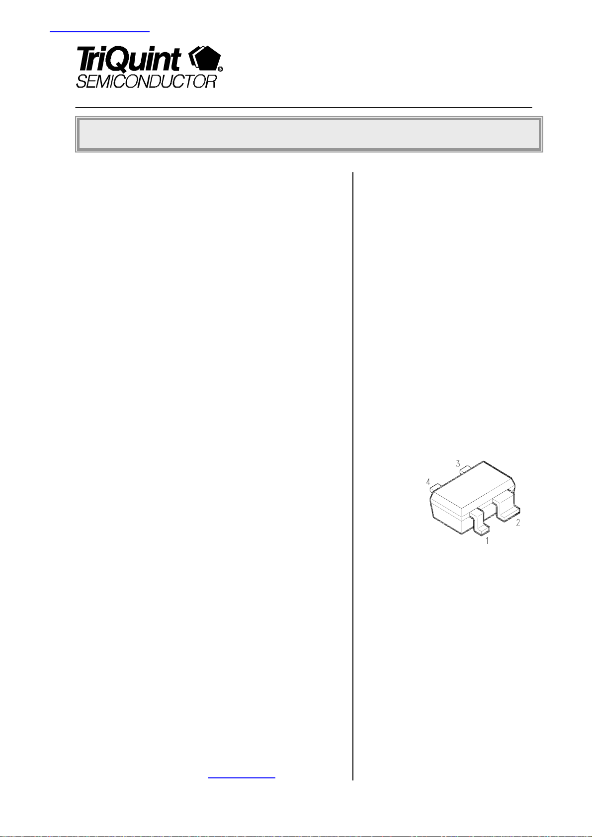
Package Outline,
SOT343:
Pin assignment:
1 = gate
2 = source
3 = drain
4 = source
For further information please visit www.triquint.com pg. 1/6
Rev. 1.2; May 29th, 2003
CFH 400 Preliminary Datasheet
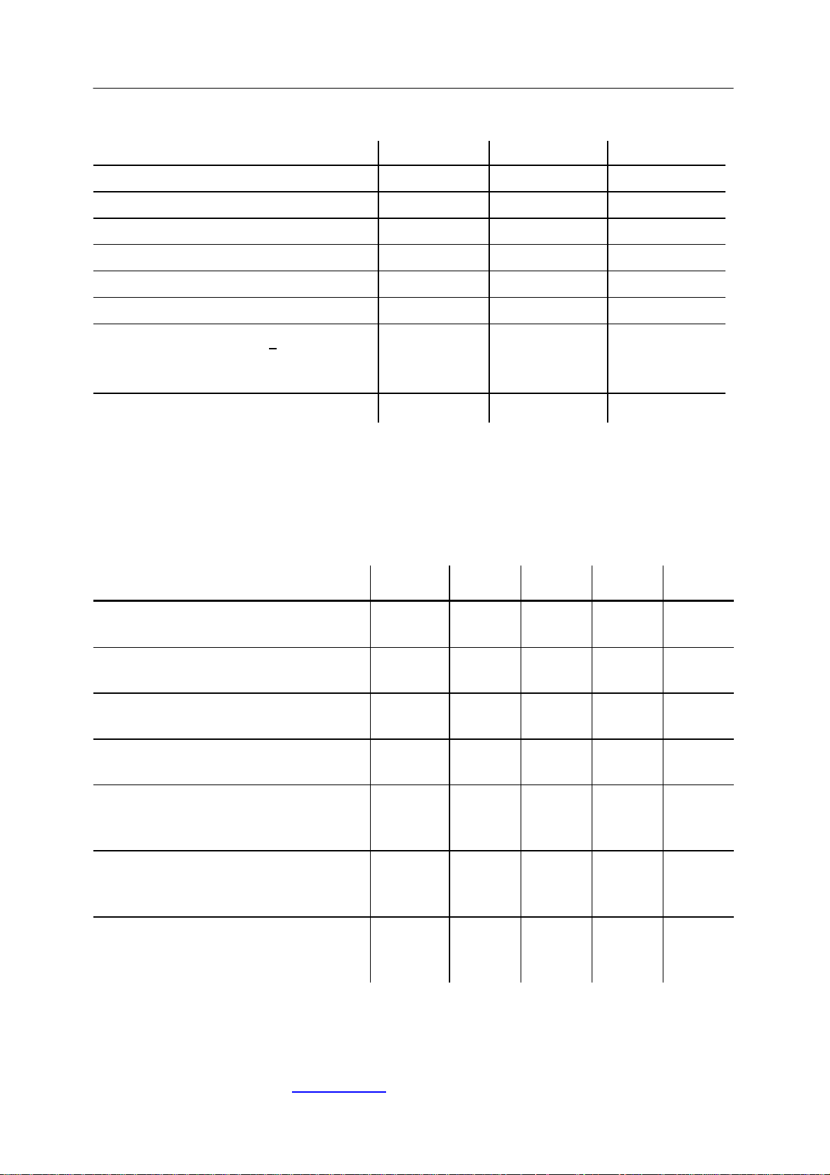
Maximum Ratings:
Parameter Symbol Unit
Drain-source voltage VDS 5.5 V
Drain-gate voltage VDG 6.5 V
Gate-source voltage VGS -2.0 V
Drain current ID 80 mA
Channel temperature TCh 150 °C
Storage temperature range T
Total power dissipation (TS < tbd°C) 2
-65...+150 °C
stg
P
150 mW
tot
Thermal resistance
Channel-soldering point source R
1) Dimensions see page 4
2) TS: Temperature measured at soldering point
thChS
166 K/W
Electrical characteristics:
at TA = 25°C unless otherwise specified
Characteristics Symbol min typ max Unit
Drain-source saturation current
VDS = 3 V VGS = 0 V
Pinch-off voltage
VDS = 3 V ID = 1 mA
Gate leakage current
VDS = 3 V ID = 15 mA
I
DSS
V
GS(P)
IG
0
-0.7
-
40
-0.25
-
70
0
5
mA
V
µA
Transconductance
VDS = 3 V ID = 15 mA
Noise figure*
VDS = 3 V ID = 10 mA f = 1.8 GHz
VDS = 3 V ID = 15 mA f = 1.8 GHz
Associated gain*
VDS = 3 V ID = 10 mA f = 1.8 GHz
VDS = 3 V ID = 15 mA f = 1.8 GHz
IIP3*
VDS = 3 V ID = 10 mA f = 1.8 GHz
VDS = 3 V ID = 15 mA f = 1.8 GHz
gm
F
Ga
IIP3
70
-
-
-
100
0.55
0.53
15.7
16.2
6
8.5
-
-
-
-
* Parameters are measured at input impedance for minimum noise figure and output
impedance for maximum gain.
For further information please visit www.triquint.com
Rev. 1.2; May 29th, 2003
pg. 2/6
mS
dB
dB
dBm
 Loading...