

TriQuint AP562-F Schematics
AP562
3.3-3.8 GHz WiMAX 8W Power Amplifier
Product Features
• 3.3 – 3.8 GHz
• +39.4 dBm P1dB
• 11.5 dB Gain
• 2.0% EVM @ 30 dBm Pout
• +12 V Supply Voltage
• Lead-free/green/RoHS-compliant
5x6 mm power DFN package
Applications
• WiMAX CPE/BTS
Specifications
Parameter Units Min Typ Max
Operational Bandwidth GHz 3.3 3.8
Test Frequency GHz 3.5
Output Channel Power dBm +30
Power Gain dB 11.5
Input Return Loss dB 15
Output Return Loss dB 6.7
Error Vector Magnitude % 1.9
Operating Current, Icc mA 685
RF Switching Speed ns 50
Collector Efficiency % 11.7
Output P1dB dBm 39.4
Quiescent Current, Icq mA 400
(4)
Vpd
V +5
Vcc V +12
Notes:
1. Test conditions unless otherwise noted: T = 25ºC, Vpd = +5V, Vcc = +12, Icq = 400mA at Pout = +30
dBm and f = 3.5 GHz.
2. Using an 802.16-2004 OFDMA, 64QAM-1/2,1024-FFT, 20 symbols, 30 subchannels signal, 9.5 d B
PAR @ 0.01%.
3. Switching speed: 50% TTL to 100/0% RF.
4. Vpd used for device power down. (low=RF off)
5. Capable of handling 10:1 VSWR @ 12 V
, WiMax signal, Pout
DC
The AP562 is a high dynamic range broadband power
amplifier in a surface mount package. The single-stage
amplifier has 11.5 dB gain, while being able to achieve
high performance for 3.3–3.8 GHz WiMAX applications
with up to 39.4 dBm of compressed 1dB power.
The AP562 uses a high reliability +12V InGaP/GaAs HBT
process technology. The device incorporates proprietary
bias circuitry to compensate for variations in linearity and
current draw over temperature. The device does not require
any negative bias voltage; an internal active bias allows the
AP562 to operate directly off a commonly used +12V
supply and has the added feature of a +5V power down
control pin. RoHS-compliant 5x6mm DFN package is
surface mountable to allow for low manufacturing costs to
the end user.
The AP562 is targeted for use in a balanced or single ended
configuration for WiMAX applications where high linearity
and high power is required.
Absolute Maximum Rating
Parameter Rating
Pin max (CW into 50Ω load)
Storage Temperature -55 to +125 ºC
Max Junction Temperature, T
Thermal Resistance, Θ
Operation of this device above any of these parameters may cause permanent damage.
TriQuint Semiconductor, Inc • Phone 1-800-9 51- 44 01 • FAX: 408-577-6633 • e-mail: info-sales@tqs.com • Web site: www.TriQuint.com Page 1 of 8 May 2009
JC
158 ºC
J,max
+33 dBm
8.4 °C / W
Product Description
Typical Performance
Parameter Units Typical
Test Frequency GHz 3.4 3.5 3.6
Channel Power dBm +30 +30 +30
Power Gain dB 11.5 11.5 11.3
Input Return Loss dB 11 15 15
Output Return Loss dB 5.6 6.7 5.9
Error Vector Magnitude % 2.2 1.9 1.7
Operating Current, Icc mA 720 685 670
Collector Efficiency % 11.1 11.7 12.2
Output P1dB dBm 39.5 39.4 38.7
Quiescent Current, Icq mA 400
Vpd V +5
Vcc V +12
= 30dBm.
AVG
Ordering Information
Part No. Description
AP562-F WiMAX 12V 8W HBT Amplifier
AP562-PCB3500 3.4-3.6 GHz Fully Assembled Evaluation Board
Standard T/R size = 500 pieces on a 7” reel.
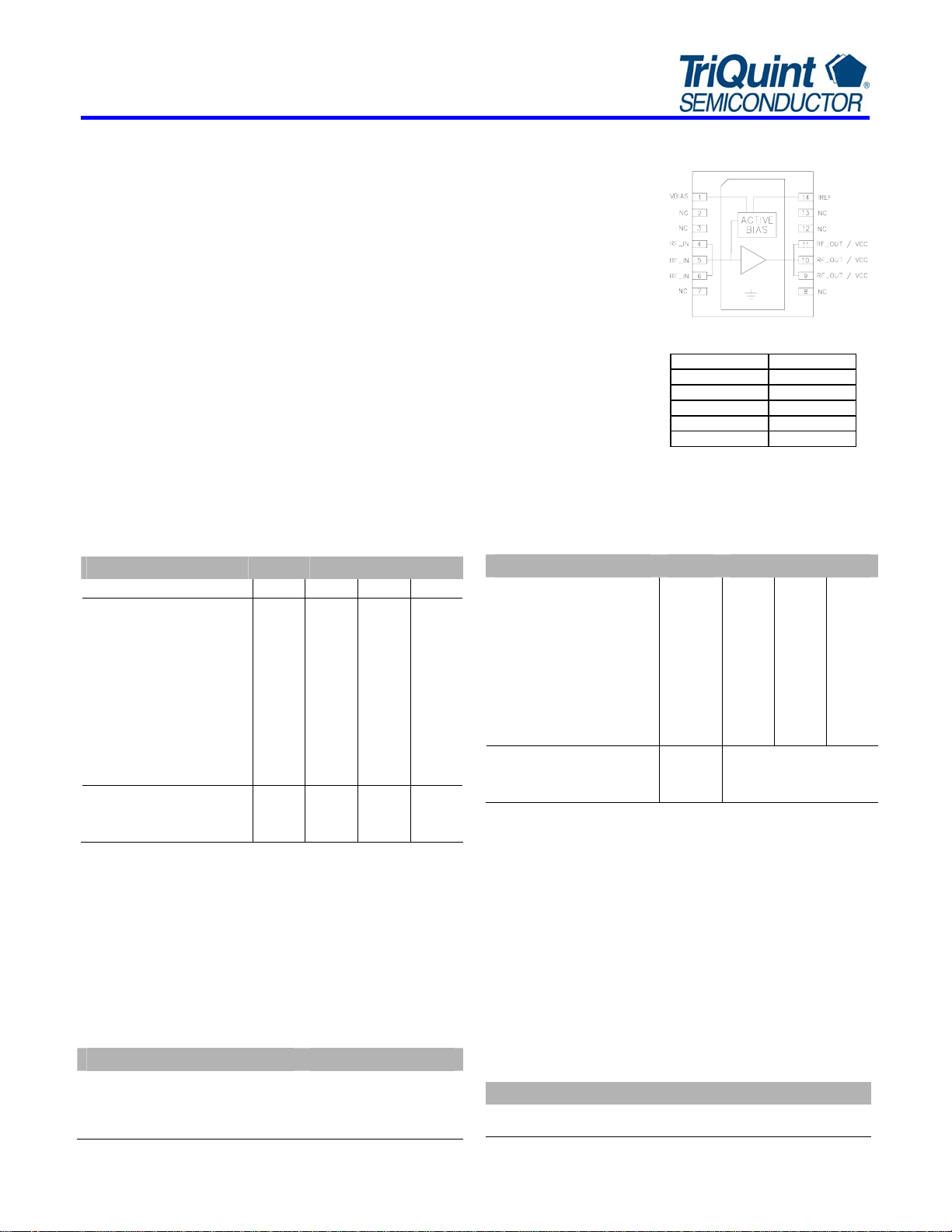
Functional Diagram
Function Pin No.
RFIN 4,5,6
RF
9,10,11
OUT
I
14
REF
V
1
BIAS
NC 2,3,7,8,12,13
Specifications and information are subject to change without notice
AP562
3.3-3.8 GHz WiMAX 8W Power Amplifier
Application Circuit PC Board Layout
Vcc
Vpd
GND
Circuit Board Material: 0.0147” Rogers Ultralam 2000, single layer, 1 oz
copper, ε
= 2.45, Microstrip line details: width = .042”, spacing = .050”
r
Notes:
1. Please note that for reliable operation, the evaluation board will have to be mounted to a much
2. The area around the module underneath the PCB should not contain any soldermask in order to
3. For proper and safe operation in the laboratory, the power-on sequencing is recommended.
Baseplate Configuration
larger heat sink during operation and in laboratory environments to dissipate the power
consumed by the device. The use of a convection fan is also recommended in laboratory
environments.
maintain good RF grounding.
Evaluation Board Bias Procedure
Following bias procedure is recommended to ensure proper functionality of AP562 in a laboratory environment. The sequencing is not
required in the final system application.
Turn-on Sequence:
1. Attach input and output loads onto the evaluation board.
2. Turn on power supply Vcc = +12V.
3. Turn on power supply Vpd = +5V.
4. Turn on RF power.
Turn-off Sequence:
1. Turn off RF power.
2. Turn off power supply Vpd = +5V.
3. Turn off power supply Vcc = +12V.
Bias. Voltage (V)
Vcc +12
Vpd +5
TriQuint Semiconductor, Inc • Phone 1-800-9 51- 44 01 • FAX: 408-577-6633 • e-mail: info-sales@tqs.com • Web site: www.TriQuint.com Page 2 of 8 May 2009
Specifications and information are subject to change without notice
AP562
3.3-3.8 GHz WiMAX 8W Power Amplifier
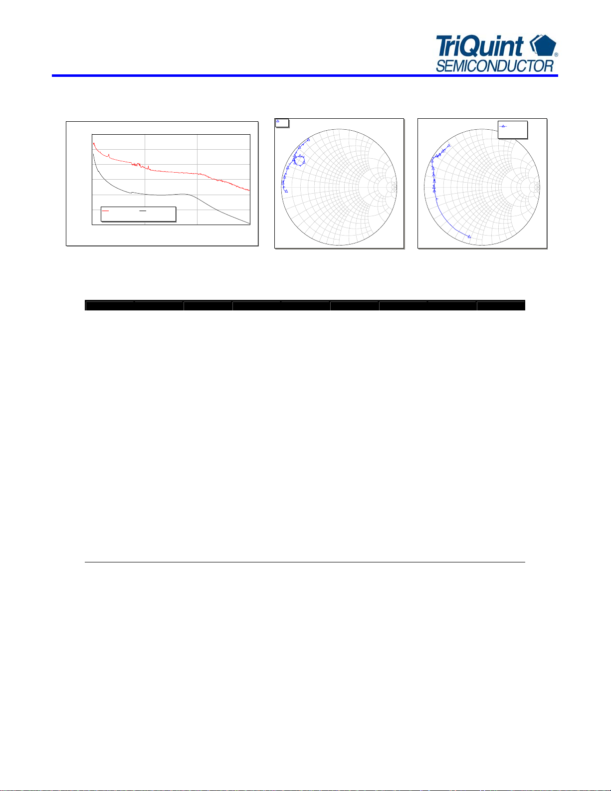
Typical Device Data
S-Parameters (VCC= +12 V, ICC = 400 mA, 25 °C, unmatched 50 ohm system)
S(1,1)
40
Gain / Maximum Stable Gain
30
20
10
Gain (dB)
0
-10
-20
DB(GMax())
AP562
0246
DB(|S(2,1)|)
AP562
Frequency (GHz)
AP562
4
.
0
2
.
0
0
0.2
2
.
0
-
4
.
0
-
Notes:
The gain for the unmatched device in 50 ohm system is shown as the trace in black color. For a tuned circuit for a particular frequency, it is expected that
actual gain will be higher, up to the maximum stable gain. The maximum stable gain is shown in the red line.
S-Parameters (VCC = +12 V, ICQ = 400 mA, 25 °C, unmatched 50 ohm system, calibrated to device leads)
Freq (MHz) S11 (dB) S11 (ang) S21 (dB) S21 (ang) S12 (dB) S12 (ang) S22 (dB) S22 (ang)
50 -0.79 -175.42 27.05 124.23 -41.01 40.51 -1.10 -104.38
100 -0.40 -177.67 22.28 107.37 -41.94 16.01 -1.53 -137.35
300 -0.31 179.53 14.07 90.92 -41.94 2.09 -1.68 -163.78
500 -0.29 177.89 9.72 82.63 -41.62 0.94 -1.77 -171.20
700 -0.29 175.84 6.87 75.39 -41.31 8.79 -1.81 -175.14
900 -0.34 173.80 4.76 69.22 -41.51 0.79 -1.71 -177.04
1100 -0.36 171.63 3.14 62.91 -41.31 -1.63 -1.63 -178.74
1300 -0.37 168.83 1.85 56.68 -41.31 -5.01 -1.60 179.84
1500 -0.35 165.93 0.86 50.02 -41.31 -8.04 -1.57 178.03
1700 -0.47 161.85 0.96 41.71 -40.35 -13.12 -1.66 174.97
1900 -0.50 158.09 0.45 34.33 -40.35 -18.22 -1.61 172.45
2100 -0.60 154.55 0.05 26.46 -40.18 -24.14 -1.51 170.10
2300 -0.69 150.84 -0.24 17.89 -40.09 -31.86 -1.38 167.43
2500 -0.82 147.61 -0.40 9.26 -39.83 -40.50 -1.28 164.93
2700 -0.94 144.72 -0.44 -0.25 -39.58 -51.10 -1.17 162.74
2900 -1.16 142.23 -0.27 -11.07 -39.33 -65.09 -1.02 160.45
3100 -1.51 140.70 -0.02 -23.54 -38.79 -81.01 -0.81 158.40
3300 -2.02 140.58 0.25 -38.88 -38.06 -102.23 -0.59 156.27
3500 -2.49 142.81 0.36 -58.18 -37.59 -129.91 -0.33 153.91
3700 -2.56 147.66 -0.16 -80.37 -37.20 -160.59 -0.23 150.78
3900 -2.06 151.40 -1.53 -102.11 -37.33 169.42 -0.28 148.13
4100 -1.43 151.78 -3.50 -120.64 -37.79 144.14 -0.40 146.26
4300 -1.01 150.24 -5.66 -135.37 -38.27 122.49 -0.53 145.38
4500 -0.76 148.06 -7.78 -147.04 -38.56 107.83 -0.64 144.44
Device S-parameters are available for download off of the website at: http://www.tqs.com
S11
8
1.0-1.0
.
0
6
.
0
1.0
0.4
0.6
0.8
6
.
0
-
8
.
0
-
Swp Max
6GHz
0
.
2
0
.
3
0
.
4
0
.
5
0
.
0
1
10.0
5.0
2.0
3.0
4.0
0
.
0
1
-
0
.
5
-
0
.
4
-
0
.
3
-
0
.
2
-
Swp Min
0.05GHz
4
.
0
2
.
0
0
0.2
2
.
0
-
4
.
0
-
S22
8
.
0
6
.
0
0.4
0.6
0.8
6
.
0
-
8
.
0
-
S(2,2)
1.0-1.0
AP562
0
.
2
1.0
5.0
2.0
3.0
4.0
0
.
2
-
Swp Max
0
.
3
4
0
0
.
3
-
Swp Min
0.05GHz
6GHz
0
.
0
.
5
0
.
0
1
10.0
0
.
0
1
-
0
.
5
-
.
4
-
TriQuint Semiconductor, Inc • Phone 1-800-9 51- 44 01 • FAX: 408-577-6633 • e-mail: info-sales@tqs.com • Web site: www.TriQuint.com Page 3 of 8 May 2009
Specifications and information are subject to change without notice
 Loading...