


TECHNICAL INFORMATION
Stereo 100W (4
using DPP
CONFIDENTIAL INFORMATION – July 1999
TM
Technology (Tornado) TA2021-100
) Class-T Digital Audio Amplifier Driver
ΩΩΩΩ
General Description
The TA2021-100 Tornado is a 100W (4Ω), two channel Amplifier Driver IC which uses
Tripath’s proprietary Digital Power Processing
both the audio fidelity of Class-AB and the power efficiency of Class-D amplifiers.
Applications
! Computer/PC Multimedia
! Video CD Players
! Cable Set Top Products
! DVD Players/Receivers
! Battery Powered Sound
Reinforcement
Benefits
! Fully Integrated Solution with
FET’s for low system cost
! Improved efficiency versus Class-AB
! Signal fidelity equal to high
quality Class-AB amplifiers
! High dynamic range compatible
with digital media such as CD,
DVD and Internet audio
! Smaller power supply due to
efficient operation
! Integrated volume control reduces
system cost and noise
! Optional control/status through
industry-standard digital serial bus
simplifies system design
TM
technology. Class-T amplifiers offer
Features
! Class-T architecture
! Integrated FET’s
! Proprietary Digital Power Processing
! “Audiophile” Sound Quality
! 0.1 % THD+N @ 100Wrms, 4
! 0.08% IHF-IM
! High Power
! 90Wrms @ 8
! High Efficiency
! 90% @90Wrms @ 8
! 85% @100Wrms @ 4
! Two modes of control/status operation:
! 1. Through analog pins
! 2. Through I
! Low Noise Floor (<150uV)
! Integrated volume control with 124dB range
controlled via I
! Programmable “Mute on Silence” feature for auto
power down
! Bridgeable, single-ended outputs
! Mute and Sleep inputs
! Headphone/Line outputs
! Turn-on & turn-off pop suppression
! Over-current & temperature protection
! Over and under-voltage protection
! Supports 100kHz BW Super Audio CD and DVD-
Audio (See App Note for specifics)
! 32-pin SSIP (Staggered Single In Line Package)
, 10% THD+N
Ω
Ω
Ω
2
C digital serial bus
2
C bus or DC input
Ω
1
TECHNICAL INFORMATION
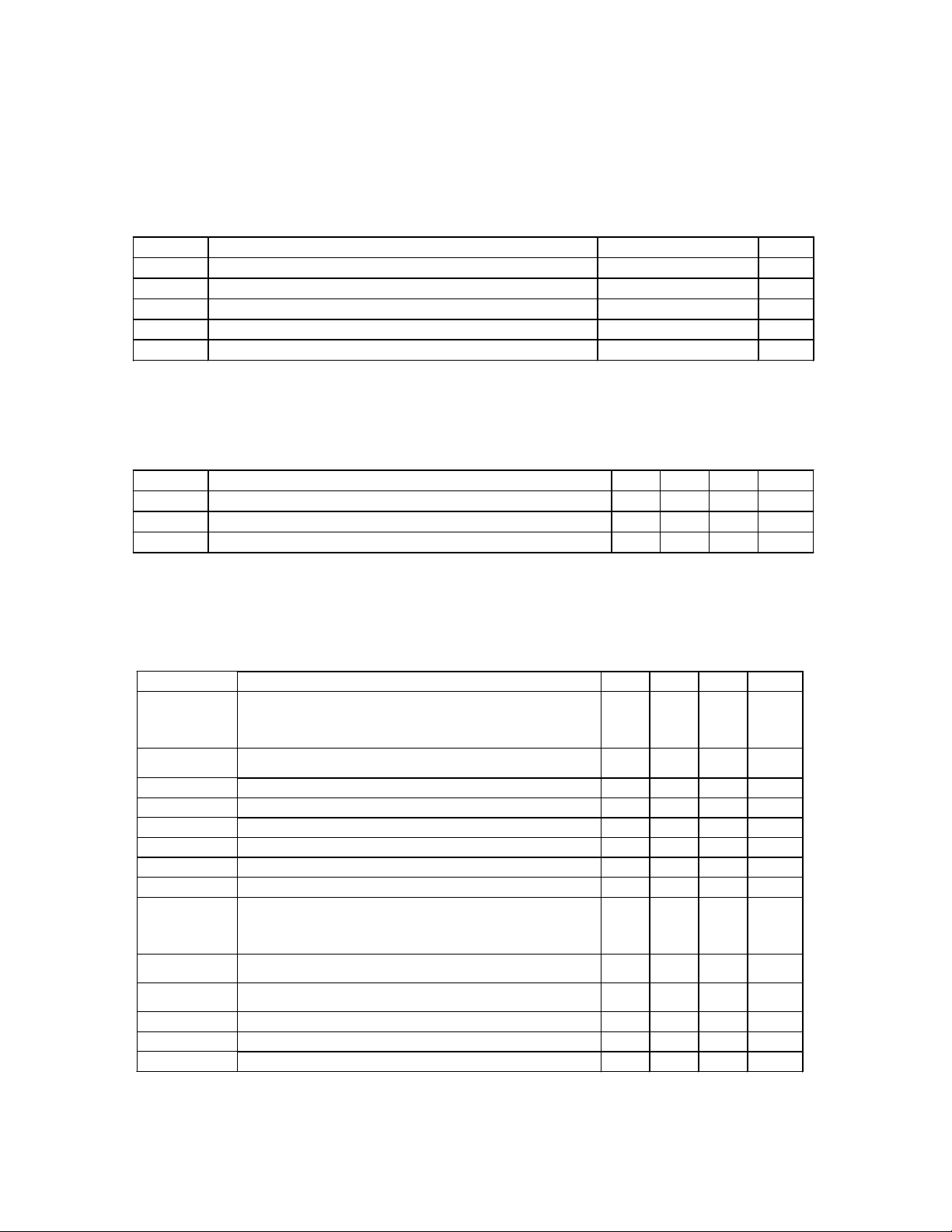
Absolute Maximum Ratings
SYMBOL PARAMETER Value UNITS
Vs Supply Voltage (Vspos & V sneg) +/-50 V
V5 Positive 5 V Bias Supply 6 V
VGG Internally generated voltage 12 V
T
STORE
T
A
Notes: Absolute Maximum Ratings indicate limits beyond which damage to the device may occur.
Operating Conditions
SYMBOL PARAMETER MIN. TYP. MAX. UNITS
Vs Supply Voltage (Vspos & V sneg) +/- 25 +/- 35 +/- 45 V
V5 Positive 5 V Bias Supply 4.5 5 5.5 V
VGG Internally Generated Voltage 10 11 12 V
Storage Temperature Range -40 to 150 ºC
Operating Free-air Temperature Range -20 to +80 ºC
Damage will occur to the device if VN10 is not supplied or falls below the recommended
operating voltage when V
is within its recommended operating range.
S
Note: Recommended Operating Conditions indicate conditions for which the device is functional. See
Electrical Characteristics for guaranteed specific performance limits.
Electrical Characteristics
TA = 25°C. See Notes 1 & 2 for Operating Conditions and Test/Application Circuit Setup.
SYMBOL PARAMETER MIN. TYP. MAX. UNITS
I
q
Quiescent Current +35V
(no load) -35V
+5V
VN12
I
S
I5
IVGG
Source Current @ P
= 100W, RL = 4ΩV
OUT
@ 10% THD+N V
Source Current for 5V Bias Supply @ P
Source Current for VGG Supply @ P
OUT
= 100W, RL = 4
OUT
= +35V
SPOS
= -35V
SNEG
= 100W, RL = 4
Ω
Ω
Vu Under Voltage (Vspos & Vsneg) 25 V
Vo Over Voltage (Vspos & Vsneg) 45 V
V
IH
V
IL
High-level Input Voltage (MUTE & SLEEP) 3.5 V
Low-level Input Voltage (MUTE & SLEEP) 1 V
IDDMUTE Mute Supply Current +35V
(no load) -35V
+5V
VGG
V
OH
High-level Output Voltage (HMUTE/SDA, OVERLO AD /SCL &
3.5 V
PSMUTE)
V
OL
Low-level Output Voltage (HMUTE/SDA, OVERLOAD/S CL &
PSMUTE)
V
TOC
A
V
Over Current Sense Voltage Threshold 1.2 V
Gain Ratio V
OUT/VIN
, RIN = 0
Ω
Voffset Offset Voltage, no load, MUTE = Logic low mV
mA
mA
mA
mA
A
A
mA
mA
mA
mA
mA
mA
1V
V/V
2
TECHNICAL INFORMATION
Minimum and maximum limits are guaranteed but may not be 100% tested.
Performance Characteristics – Single Ended
Unless otherwise specified, f = 1kHz, Measurement Bandwidth = 22kHz. TA = 25°C.
See Notes 1 & 2 for Operating Conditions and Test/Application Circuit Setup.
SYMBOL PARAMETER CONDITIONS MIN. TYP. MAX. UNITS
P
OUT
THD + N Total Harm oni c Distortion Plus
IHF-IM IHF Intermodulation Distortion
SNR Signal-to-Noise Ratio
CS Channel Separation
PSRR Power Supply Rejection Ratio Input Referenced, 30kHz Bandwidth 65 dB
η
e
NOUT
Output Power
(continuous RMS/Channel)
Noise
Power Efficiency
THD+N = 0.1%, R
THD+N = 10%, R
= 4W/Channel, RL = 4
P
OUT
19kHz, 20kHz, 1:1 (IHF), R
P
= 1W/Channel
OUT
A Weighted, R
= 100W/Channel
P
OUT
0dBr = __W, R
= 90W/Channel, RL = 8
P
OUT
= 8
Ω
L
= 4
R
Ω
L
= 8
Ω
L
= 4
R
Ω
L
= 4Ω,
L
= 4Ω, f = 1kHz
L
Ω
L
= 4
Ω
Ω
Output Noise Voltage A Weighted, no signal, input shorted,
DC offset nulled to zero
100
90
125
.02 %
0.08 %
110 dB
80 dB
90 %
150
W
W
W
W
V
µ
Minimum and maximum limits are guaranteed but may not be 100% tested.
Notes:
1) VP1=VP2=+35V, VN1=VN2=-35V, V5 = +5V, VGG = +11V referenced to PGND
3
TECHNICAL INFORMATION
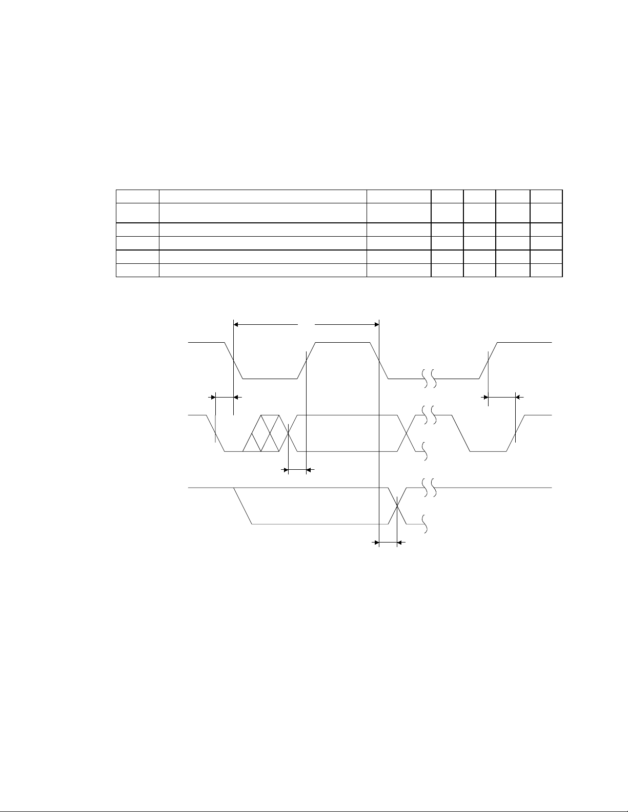
Serial Bus Timing
Unless otherwise specified, _____________
SYMBOL PARAMETER CONDITIONS MIN. TYP. MAX. UNITS
t
CL
SCL (Clock) Period
s
µ
t
SETUP
t
STABLE
t
START
t
STOP
Data In Set-up Time to SCL Low
Data Out Stable after SCL Low
SDA Low Set-up Time to SCL Low (Start Conditi on)
SDA High Hold Time after SCL Hi gh (Stop Condition)
OVERLOAD/SCL
HMUTE/SDA
(Data In)
HMUTE/SDA
(Data Out)
t
START
t
SETUP
s
µ
s
µ
s
µ
s
µ
t
CL
t
STOP
t
STABLE
4

TECHNICAL INFORMATION
Pin Description
Pin Function Description
1,13 VB2,VB1 Bootstrapped voltages supply drive to gates of high-side FET’s
2 VGG Regulated output of onboard switching regulator
3 PGND Power ground
4,12 VP2,VP1 Positive power supply connections
5 SW12V Switching node
6,11 VS2,VS1 Source voltage for high side FET’s
7,10 OUT2,OUT1 Power FET outputs
8,9 VN2,VN1 Negative power supply connections
14 SWFB Feedback for onboard regulator
15 SLEEP When set to logic high, both amplifiers are muted and in low power (idle)
16 PSMUTE A logic high output indicates the amplifiers are muted
17 OVRLD/SCL Dual function pin:
18 HMUTE/SDA Dual function pin:
19 MUTE When set to logic high, both amplifiers are muted. When set to logic low or
20 MIS/ADDR Dual function pin:
21 V5 5V power supply
22 AGND Analog Ground
23,24 INP1,INP2 Inputs for channels 1 and 2
25,26 AUXOUT1,AUXOUT2 Auxiliary outputs that provide a low impedance, buffered audio output
27 V2BG Bandgap reference
28 DCVOL When control/status of the device is via analog pins, the voltage level on this
29,31 FDBKN1,FDBKN2 Feedback for channels 1 and 2
30,32 GNDKELVIN1
GNDKELVIN2
mode. When low (grounded), both amplifiers are fully operational. If left
floating, the device stays in the mute mode. Ground if not used.
OVRLD – A logic high output indicates that the level of the input signal has
overloaded the amplifiers, signifying increased distortion
SCL – When tied to V5 through a pull-up resistor, this pin becomes the serial
clock line of the serial control bus
HMUTE – A logic high output indicates that the output stages of both
amplifiers are shut off and muted.
SDA – When OVRLD/SCL is tied to V5 through a pull up resistor, this pin
becomes the serial data line of the serial control bus
grounded both amplifiers are fully operational. Ground if not used.
MIS – When control/status of the device is via analog pins, the voltage level
ion this pint sets the Mute-in –silence threshold
ADDR – When OVRLD/SCL is tied to V5 through a pull up resistor, the voltage
on this pin selects the chip address of the device for the serial control bus
where the signal level is set by the volume control
pin sets the output signal volume
Kelvin connection to speaker ground channels 1 and 2
5

TECHNICAL INFORMATION
32-pin SSIP Package
(Top View)
1
VB2
2
VGG
3
PGND
4
VP2
5
SW12
6
VS2
7
OUT2
8
VN2
9
VN1
10
OUT1
11
VS1
12
VP1
13
VB1
14
SWFB
MUTE
INP1
INP2
V2BG
15
16
17
18
19
20
V5
21
GA
22
23
24
25
26
27
28
29
30
31
32
SLEEP
PSMUTE
OVRLD/SCL
HMUTE/SDA
MIS/ADDR
AUXOUT1
AUXOUT2
DCVOL
FDBKN1
GNDKELVIN1
FDBKN2
GNDKELVIN2
6
TECHNICAL INFORMATION
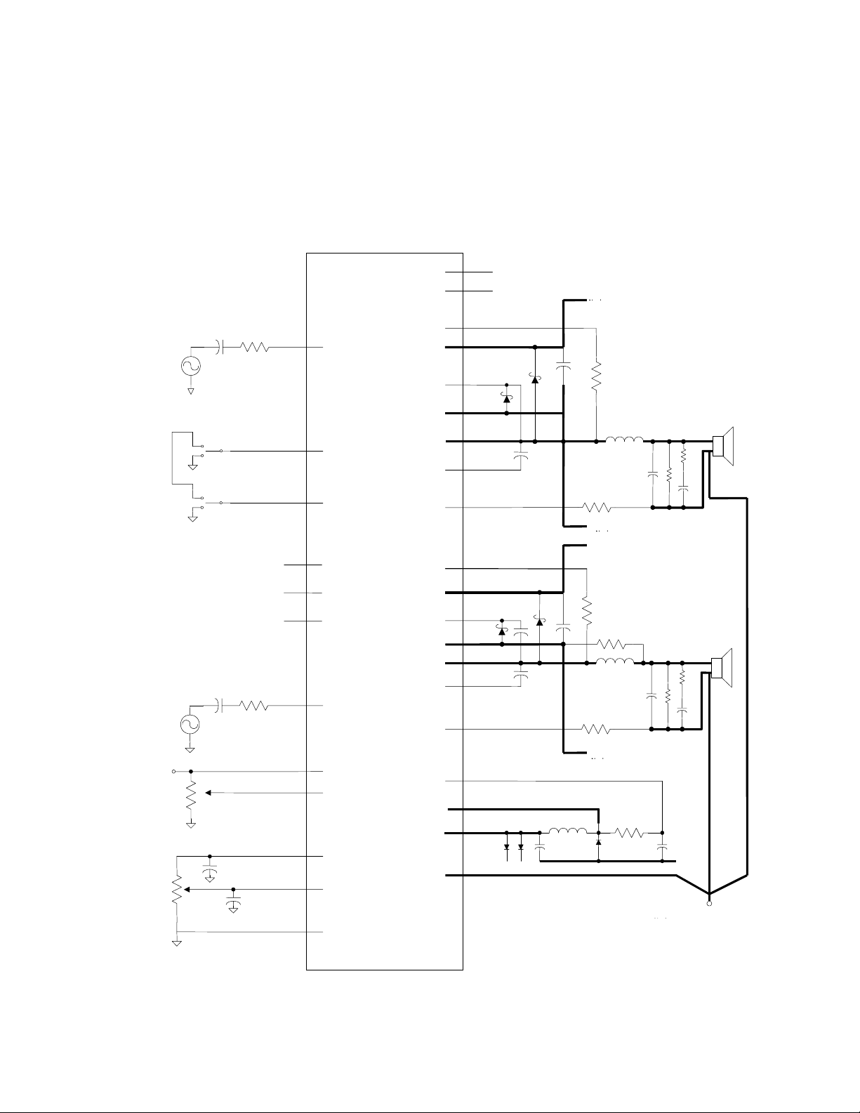
Test/Application Circuit
TA2021-100
25
26
C
IN
INP1
23
R
IN
29
12
11
V5
15
SLEEP
10
13
19
OVRLD/SCL
HMUTE/SDA
C
IN
PSMUTE
R
IN
MUTE
INP2
16
17
18
24
30
31
32
FDBKN1
VP1
VS1
VN1
9
OUT1
VB1
GNDKELVIN1
FDBKN2
VP2
4
6
VS2
8
VN2
OUT2
7
VB2
1
GNDKELVIN2
AUXOUT1
AUXOUT2
Positive Supply Star
L
F
C
F
R
G
Negative Supply Star
Positive Supply Star
L
F
C
F
R
G
R
D
R
L
C
D
R
D
R
L
C
D
+5V
V5
21
MIS/ADDR 19
27
V2BG
28
DCVOL
24
AGND
Note - Heavy Lines Indicate High-Current Paths
SW-FB14
SW12
5
VGG
2
3PGND
VB1 VB2
Negative Supply Star
VN
Power Supply Ground Star
7

TECHNICAL INFORMATION
Modes of Operation
The TA2021-100 has two modes of operation: Mode 1, where control/status of the amplifier is
by signals on analog pins of the TA2021-100, and Mode 2, where control/status of the amplifier
is by registers accessed through a digital serial control bus. When OVRLD/SCL is tied to V5
through a 5 KΩ resistor and the TA2021-100 senses this during power-up it will go into Mode 2
operation. Otherwise the TA2021-100 will use Mode 1 operation. The operating description in
this section explains operation of the TA2021-100 in Mode 1. Mode 2 operation is described in
the next section.
TA2021-100 Basic Amplifier Operation
The audio input signal is fed to the processor internal to the TA2021-100, where a modulation
pattern is generated. This pattern is spread spectrum and varies between approximately
200kHz and 1.5MHz. Complementary copies of the switching pattern are level-shifted by
MOSFET drivers which drive the gates of internal power MOSFETs that are connected as a half
bridge. The output of the half bridge is a power-amplified version of the switching pattern
that switches between VP and VN. This signal is then low-pass filtered to obtain amplified
audio.
The processor portion of the TA2021-100 is operated from a 5-volt supply (between V5 and
GND). In the generation of the complementary modulation pattern for the output MOSFETs,
the processor inserts a “break-before-make” dead time between when it turns one transistor
off and it turns the other one on in order to minimize shoot-through currents in the MOSFETs.
Feedback information from the output of the half-bridge is supplied to the processor via
FDBKN1. Additional feedback information to account for ground bounce is supplied via
GNDKELVIN1.
The MOSFET drivers in the TA2021-100 are operated from voltages obtained from VGG for the
low-side driver, and VB1 for the high-side driver. VGG must be a stable 12V above VN. The
TA2021-100 provides switching regulator circuitry to supply VGG and VB1.
Over- and Under-Voltage Protection
The TA2021-100 senses the power rails for over- and under-voltage conditions. The over- and
under-voltage limits are Vo and Vu respectively as specified in the Electrical Characteristics
table. If the supply voltage exceeds Vo or drops below Vu, the TA2021-100 shuts off the
output stages of the amplifiers and asserts a logic level high on HMUTE/SDA. The removal of
the over-voltage or under-voltage condition returns the TA2021-100 to normal operation and
returns HMUTE/SDA to a logic level low. Please note that the limits specified in the Electrical
Characteristics table are at 25°C and these limits may change over temperature.
Over-current Protection
The TA2021-100 has over-current protection circuitry to protect itself and the output transistors
from short-circuit conditions. The TA2021-100 uses the voltage across a resistor that is in series
with each output MOSFET to detect an over-current condition.
8

TECHNICAL INFORMATION
When the voltage drop becomes greater than V
(approximately 0.7V) the TA2021-100 will
OC-LIMIT
try to limit the current by internally decreasing the gain of the input stage of the TA2021-100.
If the voltage drop continues to increase to greater than V
(approximately 1.2V) the TA2021-
OC-SD
100 will shut off the output stages of its amplifiers and supply a logic level high on
HMUTE/SDA. The occurrence of an over-current condition is latched in the TA2021-100 and can
be cleared by toggling the MUTE input or cycling power.
Mute
When a logic high signal is supplied to MUTE, both amplifier channels are muted (both highand low-side transistors are turned off) and a logic level high is output on the HMUTE/SDA pin.
When a logic level low is supplied to MUTE, both amplifiers are fully operational and a logic
level low is supplied on HMUTE/SDA. There is a delay of approximately 200 milliseconds
between the de-assertion of MUTE and the un-muting of the TA2021-100.
Mute-in-silence
The TA2021-100 will automatically mute both channels when the sum of the audio signal
supplied to both of its inputs is below a preset level for approximately 340 seconds. The preset
audio level is determined by the voltage on the MIS/ADDR pin according to the following table
(The MIS/ADDR pin also determines the input-limit level, as described in the next section):
MIS/ADDR Pin Voltage
MIS Level Input-limit Level
(Fraction of V5)
0.00 – 0.05 -80dB 76%
0.05 – 0.10 -80dB 79%
0.10 – 0.15 -80dB 85%
0.15 – 0.20 -80dB 100%
0.20 – 0.25 -74dB 76%
0.25 – 0.30 -74dB 79%
0.30 – 0.35 -74dB 85%
0.35 – 0.40 -74dB 100%
0.40 – 0.45 -68dB 75%
0.45 – 0.50 -68dB 79%
0.50 – 0.55 -68dB 85%
0.55 – 0.60 -68dB 100%
0.60 – 0.65 -62dB 75%
0.65 – 0.70 -62dB 79%
0.70 – 0.75 -62dB 85%
0.75 – 0.80 -62dB 100%
0.80 – 0.85 MIS Off 75%
0.85 – 0.90 MIS Off 79%
0.90 – 0.95 MIS Off 85%
0.95 – 1.00 MIS Off 100%
9

TECHNICAL INFORMATION
The TA2021-100 will quickly automatically come out of mute when it detects that the input
signal has gone above the preset level.
Input Limit
To “soften” the clipping characteristics of the TA2021-100 it will limit the audio signal to a predetermined, programmable input-limit level according to the voltage on the MIS/ADDR pin as
specified in the previous table. This limit is a percentage of the maximum possible output level.
Overload
When logic low, the OVRLD/SCL pin indicates that the level of the input signal has overloaded
the amplifier and that the audio output signal is starting to distort. The OVRLD/SCL signal is
active only while an overload is present. The OVRLD/SCL signal can be used to control a
distortion indicator light or LED through a simple buffer circuit.
Sleep
When a logic high signal is supplied to SLEEP, both amplifier channels are shut down and the
TA2021-100 is put into a low quiescent-current mode. When a logic level low is supplied to
MUTE, both amplifiers are fully operational.
Volume Control
A 5 MΩ potentiometer is used between V2BG, DCVOL and AGND (analog ground) to control
the output volume of both channels. When DCVOL is at the same level as V2BG, the output
volume is at –6 dB. When DCVOL is at the same level as GND, the output volume is at the
minimum, or –119.5 dB.
Auxiliary Outputs
The outputs AUXOUT1 and AUXOUT2 are analog-signal audio outputs in which the signal level
is controlled by the volume control. These outputs are capable of driving approximately 15mW
each into 20-ohm loads. These outputs are still active when the TA2021-100 is in mute mode,
even if the TA2021-100 is muted because no speaker is connected (see next section).
Speaker Detect
On power-up the TA2021-100 checks to make sure that speakers are connected to prevent
damage. If a speaker is not detected on either channel on power-up, the TA2021-100 keeps the
output stages of both amplifiers shut down (in mute) and signifies this fact by asserting a logic
level one on HMUTE/SDA. The TA2021-100 will come out of mute when speakers are
connected, even after a relatively long period of time (minutes after power-up).
10

TECHNICAL INFORMATION
Functional Description – Mode 2
Serial Bus Operation
When OVRLD/SCL is tied to V5 to a 5 kΩ resistor and the TA2021-100 senses this during powerup it will go into Mode 2 operation, where control/status of the amplifier is by registers
accessed through a digital serial control bus. This serial bus is compatible with Philips’ I
The TA2021-100 operates as a slave device on the bus. The OVRLD/SCL line is an input (no clock
is generated by the TA2021-100) and the HMUTE/SDA line is a bi-directional serial data path.
Six simple operations with the two lines of the serial bus are used for transmitting to or
receiving from a TA2021-100:
1. Start bit: A high-to-low transition of the data line while the clock line is in a high
state
2. Seven-bit slave address: The first seven bits following a start bit (MSB first)
3. Read/write bit which defines whether the slave is a transmitter or receiver: The next
bit immediately after the address is the direction of the transfer. A 0 indicates that
the master will write information to the slave. A 1 indicates that the master will
receive data from the slave.
4. Acknowledge bit: Every eight-bit byte transferred (including the eight bits
comprising the address and read/write bit) is followed by an acknowledge bit from
the receiver (the master generates all clock pulses). The transmitter releases the
data line during the acknowledge clock pulse. If there was no error detected, the
receiver will pull down the SDA line during the high period of the acknowledge
clock pulse. If a slave receiver is not able to acknowledge, the slave will keep the
SDA line high and the master can then generate a stop bit to abort the transfer. If a
master receiver keeps the SDA line high during the acknowledge clock pulse the
master is signaling the end of data transmission and the slave transmitter releases
the data line to allow the master to generate a stop bit.
5. Message bits divided into eight-bit bytes: One bit is transferred during each clock
pulse. The data must be stable during the high period of the clock. The data line
can only change when the clock line is low. The MSB of the byte is transmitted first.
6. Stop bit: A low-to-high transition of the data line while the clock line is in a high
state.
2CTM
bus.
Slave ID Address
The TA2021-100 has a seven-bit slave ID address. The five most-significant bits of the slave
address are hardwired inside the TA2021-100 and are 10000. The two least-significant bits are
determined by the voltage on the MIS/ADDR pin according to the following table:
MIS/ADDR Pin Voltage
(Fraction of V5)
0.00 – 0.25 A1 = 0, A0 = 0
0.25 – 0.50 A1 = 0, A0 = 1
0.50 – 0.75 A1 = 1, A0 = 0
0.75 – 1.00 A1 = 1, A0 = 1
Address
11

TECHNICAL INFORMATION
The complete slave address is:
10000A1A0
MSB LSB
Register Assignments
The registers in the TA2021-100 are selected by the eight-bit index register. At power-up the
Index register is set to zero. The seven least-significant bits of the Index register define the
register address space in the TA2021-100. When a 1 is written to the MSB of the Index register
the Index register value is auto-incremented (by 1) after each byte transfer is complete. If a 0 is
written to the MSB of the Index register the Index register value is not changed.
The following table indicates the Index register address of each register:
I6 I5 I4 I3 I2 I1 I0 Register Addressed
0000000 STATUS
0000001 FAULT
0000010 INITIAL STATE
0000011 VOLUME ADC
0000100 CONTROL
0000101 CONFIGURATION
0000110 VOLUME1 (Channel 1)
0000111 VOLUME2 (Channel 2)
00010XX
XXX1 1XX
Test
Reserved
X = Don’t care
All Test Registers/Bits should NOT be accessed as they are used for manufacturing test of the
TA2021-100 and can cause unexpected operation. All Reserved Registers/Bits are read-only with
a value of 0.
STATUS Register
ST7 ST6 ST5 ST4 ST3 ST2 ST1 ST0
Overload
Detect
Over-
current
Reserved Reserved Reserved Mute In
Silence
Muted Fault
Detect
ST7: Overload detect. When 0, indicates normal operation. When 1, indicates that
the level of the audio input signal has overloaded the amplifier and that the
audio signal is starting to distort. This bit is read/write. Writing a 0 to it will
clear it.
ST6: Over-current detect. When 0, indicates normal operation. When 1, indicates
that the voltage across R
has become greater than V
S
, indicating an over-
OC-LIMIT
current condition and the TA2021-100 is attempting to limit the current by
decreasing the input level using the volume control. This bit is read/write.
Writing a 0 to it will clear it.
12

TECHNICAL INFORMATION
ST5: Reserved. Read-only with a value of 0. Writing to it has no effect.
ST4: Reserved. Read-only with a value of 0. Writing to it has no effect.
ST3: Reserved. Read-only with a value of 0. Writing to it has no effect.
ST2: Mute In Silence. When 0, indicates normal operation. When 1, indicates the sum
of the input levels of both channels is below the specified level for the
specified duration. This bit is read-only. Writing to it has no effect.
ST1: Muted. When 0, indicates normal operation. When 1, indicates both outputs
are muted either due to an external control request or a fault condition has
been detected. This bit is read-only. Writing to it has no effect.
ST0: Fault. When 0, indicated normal operation. When 1, indicates a fault has been
Detected. This bit is read-only. Writing to it has no effect.
FAULT Register
F7 F6 F5 F4 F3 F2 F1 F0
Reserved Reserved Reserved Reserved Over-
current
fault
Power
Supply
Mute
Over-
temp.
Fault
Voltage
Fault
F7: Reserved. Read-only with a value of 0. Writing to it has no effect.
F6: Reserved. Read-only with a value of 0. Writing to it has no effect.
F5: Reserved. Read-only with a value of 0. Writing to it has no effect.
F4: Reserved. Read-only with a value of 0. Writing to it has no effect.
F3: Over-current fault. When 0, indicates normal operation. When 1, indicates that
the voltage across R
fault and the TA2021-100 has shut down the output stages of its amplifiers. This
bit is read-only. Writing to it has no effect.
F2: Power supply mute. When 0, indicates normal operation. When 1, indicates an
over-current condition has occurred, the TA2021-100 has shut down the output
stages of its amplifiers and the over-current situation still exists. This bit is readonly. Writing to it has no effect.
F1: Over-temperature fault. When 0, indicates normal operation. When 1, indicates
that the die temperature of the TA2021-100 has exceeded TBD. This bit is readonly. Writing to it has no effect.
F0: Voltage fault. When 0, indicates normal operation. When 1, indicates an over-/
under- voltage condition has shut down the TA2021-100. This bit is read-only.
Writing to it has no effect.
INITIAL STATE Register
IS7 IS6 IS5 IS4 IS3 IS2 IS1 IS0
Reserved Reserved Speaker
has become greater than V
S
Speaker
Detect
Channel
2
Detect
Channel
1
, indicating an over-current
OC-SD
Reserved Test Test Test
IS7: Reserved. Read-only with a value of 0. Writing to it has no effect.
IS6: Reserved. Read-only with a value of 0. Writing to it has no effect.
IS5: Speaker detect channel 2. When 0, indicates that a speaker has been detected.
13

TECHNICAL INFORMATION
When 1, indicates that a speaker has not been detected and the amplifier has
been muted. This bit is read-only. Writing to it has no effect.
IS4: Speaker detect channel 1. When 0, indicates that a speaker has been detected.
When 1, indicates that a speaker has not been detected and the amplifier has
been muted. This bit is read-only. Writing to it has no effect.
IS3: Reserved. Read-only with a value of 0. Writing to it has no effect.
IS2: Test. Should not be accessed.
IS1: Test. Should not be accessed.
IS0: Test. Should not be accessed.
VOLUME ADC Register
V7 V6 V5 V4 V3 V2 V1 V0
MSB LSB
V7-V0: Volume ADC. These bits provide a digital word value for the volume level set by
the voltage on the DCVOL pin. The resolution is 0.5dB per bit/step. All bits in
this register are read-only.
V7 V6 V5 V4 V3 V2 V1 V0 Volume/Gain
11111111 Maximum
XXX1XXXX Intermediate Level
00010000 Minimum
0000XXXX Minimum
CONTROL Register
CTL7 CTL6 CTL5 CTL4 CTL3 CTL2 CTL1 CTL0
Mute Sleep Input
CTL7: Mute. Writing a 0 to this bit (power-up initialization value) tells the TA2021-100
to operate normally. Writing a 1 to this bit tells the TA2021-100 to go into mute
mode, where the output stages of both amplifiers are shut down but all other
circuitry is still operational (including the volume control and AUXOUT audio
outputs. This bit is read/write.
CTL6: Sleep. Writing a 0 to this bit (power-up initialization value) tells the TA2021-100
to operate normally. Writing a 1 to this bit shuts down both amplifiers and
most other circuitry in the TA2021-100 and puts the device in a low-power
mode. This bit is read/write.
CTL5: Test. Should not be accessed.
CTL4: Test. Should not be accessed.
CTL3: Reserved. Read-only with a value of 0. Writing to it has no effect.
CTL2-CTL0: Input-limit level. The TA2021-100 will limit the audio signal to a percentage
of the maximum possible output level as specified by these bits in order to
“soften” its clipping characteristics. These bits are read/write.
Reserved Reserved Reserved Reserved Reserved
Select
14

TECHNICAL INFORMATION
CTL2 CTL1 CTL0 Input-limit Level
111 73%
110 76%
101 78%
100 79%
011 82%
010 85%
001 88%
0 0 0 100%
CONFIGURATION Register
CFG7 CFG6 CFG5 CFG4 CFG3 CFG2 CFG1 CFG0
Test Volume
Zero
Cross
CFG7: Test. Should not be accessed.
CFG6: Volume zero cross. Writing a 0 to this bit (power-up initialization value)
tells the TA2021-100 that volume changes can be made at any time. Writing a 1
to this bit tells. The TA2021-100 to only make volume changes at zero crossings
of the audio inputs.
CFG5: Volume ramp. Writing a 0 to this bit (power-up initialization value) tells the
TA2021-100 to implement any volume change requested immediately as
requested. Writing a 1 to this bit tells the TA2021-100 to implement any volume
at a rate of 40 msec per dB.
CFG4: Volume control mode. Writing a 0 to this bit (power-up initialization value) tells
the TA2021-100 to use the voltage on the DCVOL pin to directly control the
volume of both channels. Writing a 1 to this bit tells the TA2021-100 to use the
values in the VOLUME1 and VOLUME2 registers to set the output volumes of
the respective channels. This bit is read/write.
CFG3-CFG2: MIS time. These bits set the time interval during which the input
audio level must be below the specified level after which the TA2021-100 will
mute its outputs. These bits are read/write.
Volume
Ramp
Volume
Control
Mode
MIS
Time 1
MIS
Time 0
MIS
Level 1
MIS
Level 0
CFG3 CFG2 MIS Time
0 0 340 seconds (power-up initialization
value)
0 1 85 seconds
1 0 680 seconds
11
CFG1-CFG0: MIS level. These bits set the audio level below which the input signal must
be for the TA2021-100 to mute its outputs after the specified time interval.
These bits are read/write.
CFG1 CFG0 MIS Level
0 0 -80dB (power-up initialization value)
(MIS disabled)
∞
15

TECHNICAL INFORMATION
0 1 -74dB
1 0 -68dB
1 1 -62dB
VOLUME1 Register
V1R7 V1R6 V1R5 V1R4 V1R3 V1R2 V1R1 V1R0
MSB LSB
V1R7-V1R0: Volume 1 (Channel 1). These bits set the output volume level for Channel 1
when the CFG4 bit in the CONFIGURATION register is set to 1. The resolution is
0.5dB per bit/step. The power-up initialization value is all ones. All bits in this
register are read/write.
V1R7 V1R6 V1R5 V1R4 V1R3 V1R2 V1R1 V1R0 Volume/Gain
00000000Maximum (+4dB)
11110111Minimum (-119.5dB)
11111XXXMinimum (-119.5dB)
VOLUME2 Register
V2R7 V2R6 V2R5 V2R4 V2R3 V2R2 V2R1 V2R0
MSB LSB
V2R7-V2R0: Volume 2 (Channel 2). These bits set the output volume level for Channel 2
when the CFG4 bit in the CONFIGURATION register is set to 1. The resolution is
0.5dB per bit/step. The power-up initialization value is all ones. All bits in this
register are read/write.
V2R7 V2R6 V2R5 V2R4 V2R3 V2R2 V2R1 V2R0 Volume/Gain
00000000Maximum (+4dB)
11110111Minimum (-119.5dB)
11111XXXMinimum (-119.5dB)
Bus Transfer Sequences
To Be Supplied.
16

TECHNICAL INFORMATION
Application Information
Power Supplies
The TA2021-100 requires the split supply rails VP1(VP2) and VN1(VN2), and +5V(VA). It also uses
some additional voltages, VGG, V
BOOT1
and V
components for the switching regulator … To Be Supplied
Supply Voltage and Output Power
The relationship between the bipolar power supply voltage needed, VS, for a given RMS output
power, P
, into a given load, RL, at a given level of THD (total harmonic distortion) is
OUT
approximated by:
, that it generates internally. The selection of
BOOT2
V
= (2 x RL x P
S
0.5
)
/(K x RL/(RL + RON + RS + R
OUT
COIL
))
where:
= The at-temperature R
R
ON
= Resistance of the output filter inductor.
R
COIL
= Sense Resistor
R
S
of the output transistors, M.
DSON
K = THD Factor, a number fixed by the algorithms in the TA2021-100’s signal processor
that provides the relationship between THD at full output power of the amplifier
and V
. K corresponds to THD at full output power as follows:
S
THD K
0.1% 0.83
1% 0.95
10% 1.09
Bridged Operation
Note that the two channels of a TA2021-100 amplifier can be used to provide a single, bridged
amplifier of almost four times the output power of one of the single-ended amplifier channels.
To configure a bridged amplifier, the input to one TA2021-100 channel must be the inverted
signal of the input to the other channel.
Low-frequency Power Supply Pumping
A potentially troublesome phenomenon in single-ended switching amplifiers is power supply
pumping. This is caused by current from the output filter inductor flowing into the power
supply output filter capacitors in the opposite direction as a DC load would drain current from
them. Under certain conditions (usually low-frequency input signals), this current can cause the
supply voltage to “pump” (increase) and eventually cause over-voltage/under-voltage shut
down. Moreover, since over/under-voltage are not “latched” shutdowns, the effect would be
an amplifier that oscillates between on and off states.
Even though the TA2021-100 has circuitry that nulls out any DC offset on power-up, a prudent
design will comprehend the power supply pumping issue. A no-cost solution uses the fact that
music has low frequency information that is correlated in both channels (it is in phase). This
17

TECHNICAL INFORMATION
information can be used to eliminate boost by putting the two channels of a TA2021-100
amplifier out of phase with each other. This works because each channel is pumping out of
phase with the other, and the net effect is a cancellation of pumping currents in the power
supply. The phase of the audio signals needs to be corrected by connecting one of the speakers
in the opposite polarity as the other channel.
Amplifier Gain and Input Resistor Selection
The value of the input resistor, RIN, is based on the required voltage gain, AV, of the amplifier
according to:
= 800 x103/(RIN + 5000)
A
V
where R
= Input resistor value in ohms.
IN
Input Capacitor Selection
CIN can be calculated once a value for RIN has been determined. CIN and RIN determine the input
low-frequency pole. Typically this pole is set at 10 Hz. C
C
= 1/(2π x FP)(RIN + 5000)
IN
is calculated according to:
IN
where:
= Input resistor value in ohms.
R
IN
= Input low frequency pole (typically 10Hz).
F
P
DC Offset
The TA2021-100 has circuitry that nulls out any DC offset on power-up and external circuitry to
perform this function, as was necessary with the TA0102A and TA0103A, is no longer necessary.
It should be noted that the DC voltage on the output of a TA2021-100 amplifier with no load in mute mode is
approximately 2.5V. This offset does not need to be nulled. The output impedance of the amplifier in mute
mode is approximately 10 KOhms. This means that the 2.5V drops to essentially zero when a typical load is
connected.
Clamping Diodes
The purpose of the diodes across each of the output MOSFETs is to clamp the voltages the
MOSFET experiences to levels within its rating to prevent damage. Tripath recommends that
fast-recovery or schottky diodes be used for this purpose. The breakdown voltage rating of
this diode should be similar to that of the MOSFET. Also, the forward voltage drop of this
diode should be less than that of the internal body diode of the MOSFET.
Turn-on & Turn-off Noise
If turn-on or turn-off noise is present in a TA2021-100 amplifier, the cause is frequently due to
other circuitry external to the TA2021-100. While the TA2021-100 has circuitry to suppress
turn-on and turn-off transients, the combination of the power supply and other audio circuitry
with the TA2021-100 in a particular application may exhibit audible transients. One solution
18

TECHNICAL INFORMATION
that will completely eliminate turn-on and turn-off pops and clicks is to use a relay to
connect/disconnect the amplifier from the speakers with the appropriate timing at power
on/off. The relay can also be used to protect the speakers from a component failure (e.g.
shorted output MOSFET), which is a protection mechanism that some amplifiers have. Circuitry
external to the TA2021-100 would need to be implemented to detect these failures.
Output Filter Design
One advantage of Tripath amplifiers over PWM solutions is the ability to use higher-cutofffrequency filters. This means any load-dependent peaking/droop in the 20kHz audio band
potentially caused by the filter can be made negligible. This is especially important for
applications where the user may select a 4-Ohm or 8-Ohm speaker. Furthermore, speakers are
not purely resistive loads and the impedance they present changes over frequency and from
speaker model to speaker model.
Tripath recommends designing the filter as a 2nd order, 80kHz LC filter. Tripath has obtained
good results with L
The core material of the output filter inductor has an effect on the distortion levels produced
by a TA2021-100 amplifier. Tripath recommends low-mu type-2 iron powder cores because of
their low loss and high linearity.
= 18uH and CF = 0.22uF.
F
Tripath also recommends that an RC damper be used after the LC low-pass filter. No-load
operation of a TA2021-100 amplifier can create significant peaking in the LC filter, which
produces strong resonant currents that can overheat the output MOSFETs and/or other
components. The RC dampens the peaking and prevents problems. Tripath has obtained good
results with R
= 33Ω and CD = 0.1uF.
D
It is highly recommended that the design process for a TA2021-100 amplifier include an analysis
of the interaction of intended speaker(s) with the LC filter and RC damper to ensure the
desired frequency response is attained. Component values for the LC filter and RC damper may
need to be altered from the Tripath suggestions to achieve the required response.
Grounding
To Be Supplied
Circuit Board Layout
Considerable care needs to be taken in the layout of the circuit board for a TA2021-100
amplifier. The high currents flowing through PCB traces and the inductive effects due to the
switching frequencies involved can cause large overshoot and undershoot voltages if care is not
taken. A general rule to follow is to keep the PCB trace of each signal path to/from each lead
of each output MOSFET as short as physically possible.
Certain circuit functions in a TA2021-100 amplifier cannot share PCB return paths with other
functions because of the resistive and inductive effects of the switching currents and
frequencies used. These so-called ‘Kelvin’ paths must each have a dedicated PCB trace from the
TA2021-100 to their destination. GNDKELVIN1 and GNDKELVIN2 should be treated as Kelvin
paths.
19

TECHNICAL INFORMATION
Performance Measurements of a TA2021-100 Amplifier
Tripath amplifiers operate by modulating the input signal with a high-frequency switching
pattern. This signal is sent through a low-pass filter (external to the Tripath amplifier) that
demodulates it to recover an amplified version of the audio input. The frequency of the
switching pattern is spread spectrum and typically varies between 200kHz and 1.5MHz, which is
well above the 20Hz – 22kHz audio band. The pattern itself does not alter or distort the audio
input signal but it does introduce some inaudible noise components.
The measurements of certain performance parameters, particularly those that have anything to
do with noise, like THD+N, are significantly affected by the design of the low-pass filter used
on the output of the TA2021-100 and also the bandwidth setting of the measurement
instrument used. Unless the filter has a very sharp roll-off just past the audio band or the
bandwidth of the measurement instrument ends there, some of the inaudible noise
components introduced by the Tripath amplifier switching pattern will get integrated into the
measurement, degrading it.
One advantage of Tripath amplifiers is that they do not require large multi-pole filters to
achieve excellent performance in listening tests, usually a more critical factor than performance
measurements. Though using a multi-pole filter may remove high-frequency noise and
improve THD+N type measurements (when they are made with wide-bandwidth measuring
equipment), these same filters can increase distortion due to inductor non-linearity. Multi-pole
filters require relatively large inductors, and inductor non-linearity increases with inductor
value.
Efficiency Of A TA2021-100 Amplifier
The efficiency, η, of an amplifier is:
= P
η
OUT/PIN
The power dissipation of a TA2021-100 amplifier is primarily determined by the on resistance,
, of the output transistors used, and the switching losses of these transistors, PSW. For a
R
ON
TA2021-100 amplifier, P
P
IN
= P
DRIVER
+ PSW + P
(per channel) is approximated by:
IN
((RS + RON + R
OUT
+ RL)/RL)
COIL
2
where:
P
= Power dissipated in the TA2021-100 = 1.6W/channel
DRIVER
= 2 x (0.015) x Qg (Qg is the gate charge of M, in nano-coulombs)
P
SW
R
= Resistance of the output filter inductor (typically around 50mΩ)
COIL
For a 100W RMS per channel, 8Ω load amplifier using an R
P
IN
= P
DRIVER
+ PSW + P
((RS + RON + R
OUT
+ RL)/RL)
COIL
2
= 1.6 + 2 x (0.015) x (95) + 100 x ((0.025 + 0.11 + 0.05 + 8)/8)
of 50mΩ,
S
2
= 1.6 + 2.85 + 104.6
= 109.05
20

TECHNICAL INFORMATION
In the above calculation the R
order to account for some temperature rise of the MOSFETs. (R
of 0.065Ω was multiplied by a factor of 1.7 to obtain RON in
DS (ON)
typically increases by a
DS (ON)
factor of 1.7 for a typical MOSFET as temperature increases from 25ºC to 170ºC.)
So,
η
= P
= 100/109.05 = 92%
OUT/PIN
This compares favorably to the measured efficiency (see Typical Performance graphs).
21

TECHNICAL INFORMATION
Package Information
32-pin SSIP
22

TECHNICAL INFORMATION
ADVANCED DEVELOPMENT – This is a product in development. Tripath Technology Inc. reserves
the right to make any changes without further notice to improve reliability, function or design.
This data sheet contains the design specifications for a product in development. Specifications may
change in any manner without notice. Tripath and Digital Power Processing are trademarks of
Tripath Technology Inc. Other trademarks referenced in this document are owned by their
respective companies
Tripath Technology Inc. reserves the right to make changes without further notice to any products
herein to improve reliability, function or design. Tripath does not assume any liability arising out of
the application or use of any product or circuit described herein; neither does it convey any license
under its patent rights, nor the rights of others.
.
TRIPATH’S PRODUCTS ARE NOT AUTHORIZED FOR USE AS CRITICAL COMPONENTS IN LIFE SUPPORT
DEVICES OR SYSTEMS WITHOUT THE EXPRESS WRITTEN CONSENT OF THE PRESIDENT OF TRIPATH
TECHNOLOGY INC.
As used herein:
1. Life support devices or systems are devices or systems which, (a) are intended for surgical
implant into the body, or (b) support or sustain life, and whose failure to perform, when properly
used in accordance with instructions for use provided in this labeling, can be reasonably expected
to result in significant injury to the user.
2. A critical component is any component of a life support device or system whose failure to
perform can be reasonably expected to cause the failure of the life support device or system, or to
affect its safety or effectiveness.
TRIPATH TECHNOLOGY INC.
3900 Freedom Circle, Santa Clara, California 95054, 1-408-567-3000.
WWW.TRIPATH.COM
23
 Loading...