

TRIPATH TECHNOLOGY TA1101B Datasheet
TECHNICAL INFORMATION
Stereo 10W (4ΩΩΩΩ) Class-T™ Digital Audio Amplifier using
Digital Power Processing™ Technology TA1101B
September 2000
General Description
The TA1101B is a 10W continuous average two-channel Class-T Digital Audio Power
Amplifier IC using Tripath’s proprietary Digital Power Processing™ technology. Class-T
amplifiers offer both the audio fidelity of Class-AB and the power efficiency of Class-D
amplifiers.
Applications
!"Computer/PC Multimedia
!"DVD Players
!"Cable Set-Top Products
!"Televisions
!"Video CD Players
!"Battery Powered Systems
Benefits
!"Fully integrated solution with FETs
!"Easier to design-in than Class-D
!"Reduced system cost with no heat sink
!"Dramatically improves efficiency versus
Class-AB
!"Signal fidelity equal to high quality linear
amplifiers
!"High dynamic range compatible with digital
media such as CD, DVD, and Internet audio
Typical Performance
Features
!"Class-T architecture
!"Single Supply Operation
!"“Audiophile” Quality Sound
!"0.04% THD+N @ 9W, 4Ω
!"0.18% IHF-IM @ 1W, 4Ω
!"6W @ 8Ω, 0.1% THD+N
!"11W @ 4Ω, 0.1% THD+N
!"High Power
!"10W @ 8Ω, 10% THD+N
!"15W @ 4Ω, 10% THD+N
!"High Efficiency
!"88% @ 10W, 8Ω
!"81% @ 15W, 4Ω
!"Dynamic Range = 102 dB
!"Mute and Sleep inputs
!"Turn-on & turn-off pop suppression
!"Over-current protection
!"Over-temperature protection
!"Bridged outputs
!"30-pin Power SOP package
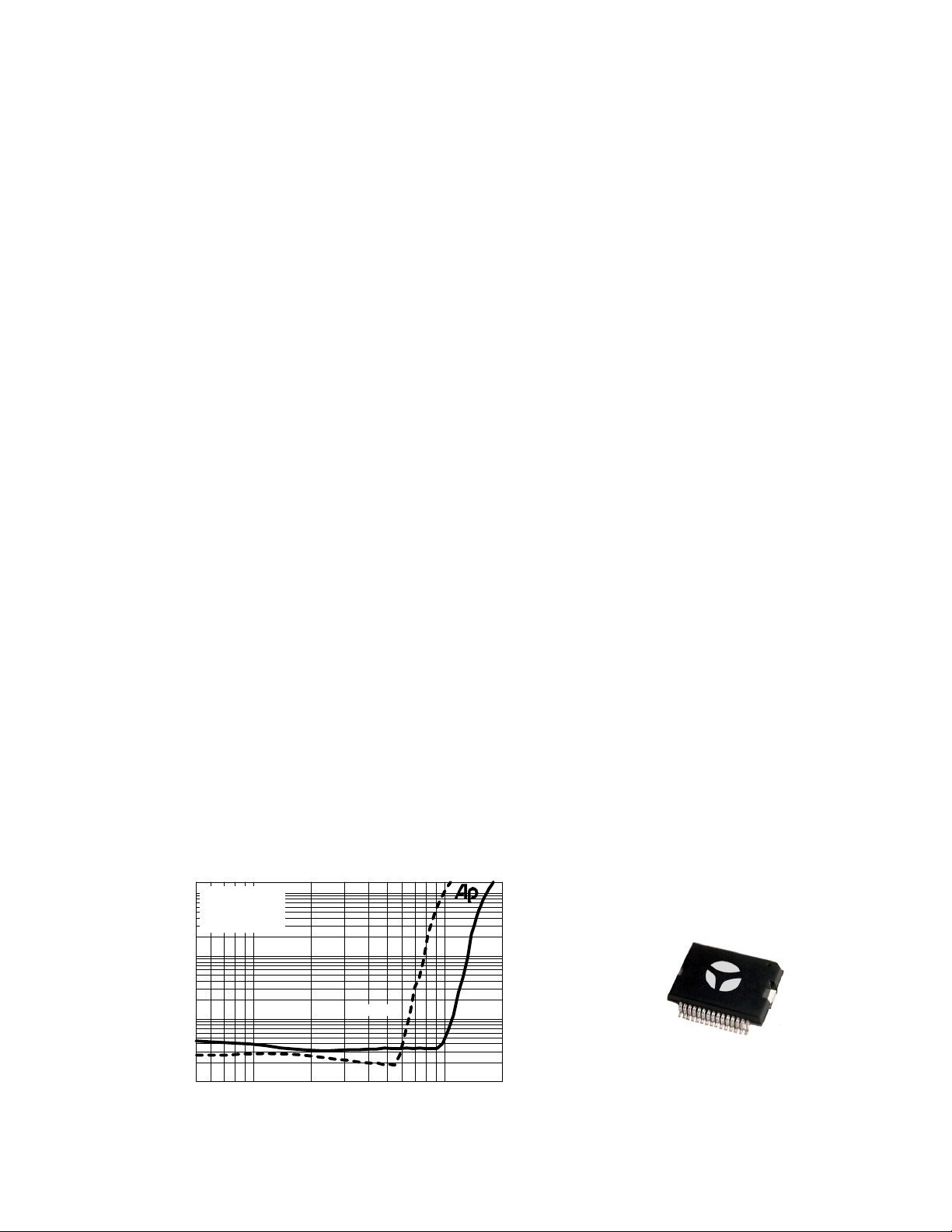
10
VDD = 12V
f = 1kHz
5
Av = 12
BW = 22Hz - 22kHz
2
1
0.5
0.2
THD+N (%)
0.1
0.05
0.02
0.01
THD+N versus Output Power
1 2 5 10 20500m
Output Power (W)
RL= 8
RL= 4
Ω
Ω
TA1101B, Rev. 2.2, 08.17.00 1
TECHNICAL INFORMATION
Absolute Maximum Ratings
(Note 1)
SYMBOL PARAMETER Value UNITS
V
DD
T
STORE
T
A
P
DISS
Supply Voltage 16 V
Storage Temperature Range
Operating Free-air Temperature Range
Continuous Total Power Dissipati on Note 2 W
-40
°
0
°
to 150°
to 70°
C
C
Note 1: Absolute Maximum Ratings indicate limits beyond which damage to the device may occur.
Note 2: See Power Dissipation Derating in the Applications Information section.
Operating Conditions
(Note 3)
SYMBOL PARAMETER MIN. TYP. MAX. UNITS
V
DD
V
IH
V
IL
Supply Voltage 8.5 12 13.2 V
High-level Input Voltage (MUTE, SLEEP) 3.5 V
Low-level Input Voltage (MUTE, SLEEP ) 1 V
Note 3: Recommended Operating Conditions indicate conditions for which the device is functional. See
Electrical Characteristics for guaranteed specific performance limits.
Electrical Characteristics
See Test/Application Circuit. Unless otherwise specified, VDD = 12V, f = 1kHz, Measurement
Bandwidth = 22kHz, R
SYMBOL PARAMETER CONDITIONS MIN. TYP. MAX. UNITS
P
O
I
DD,MUTE
I
DD, SLEEP
I
q
THD + N Total Harmonic Distortion Plus
IHF-IM IHF Intermodulation Dis tortion 19kHz, 20kHz, 1:1 (IHF) 0.18 0.5 %
SNR Signal-to-Noise Ratio
CS Channel Separation 30kHz Bandwidth 50 55 dB
PSRR Power Supply Rejection Ratio Vripple = 100mV. 60 80 dB
η
V
OFFSET
VOH High-level output vol tage
VOL Low-level output voltage
e
OUT
Output Power
(Continuous Average/Channel)
Mute Supply Current MUTE = VIH 5.5 7 mA
Sleep Supply Current SLEEP = VIH 0.25 2 mA
Quiescent Current VIN = 0 V 61 75 mA
Noise
Power Efficiency
Output Offset Voltage No Load, MUTE = Logic Low 50 150 mV
(FAULT & OVERLOAD)
(FAULT & OVERLOAD)
Output Noi se Voltage A-Weighted, input AC grounded 100
Note: Minimum and maximum limits are guaranteed but may not be 100% tested.
= 4Ω, TA = 25 °C, Package heat slug soldered to 2.8 square-inch PC pad.
L
9
THD+N = 0.1% R
R
THD+N = 10% R
R
PO = 9W/Channel 0.04 %
A-Weighted, P
= 10W/Channel, RL = 8Ω
P
OUT
3.5 V
1 V
= 4Ω
L
= 8Ω
L
= 4Ω
L
= 8Ω
L
= 1W, RL = 8Ω
OUT
5.5
12
89 dB
11
6
16
8
10
88 %
W
W
W
W
V
µ
2 TA1101B, Rev. 2.2, 08.17.00
TECHNICAL INFORMATION
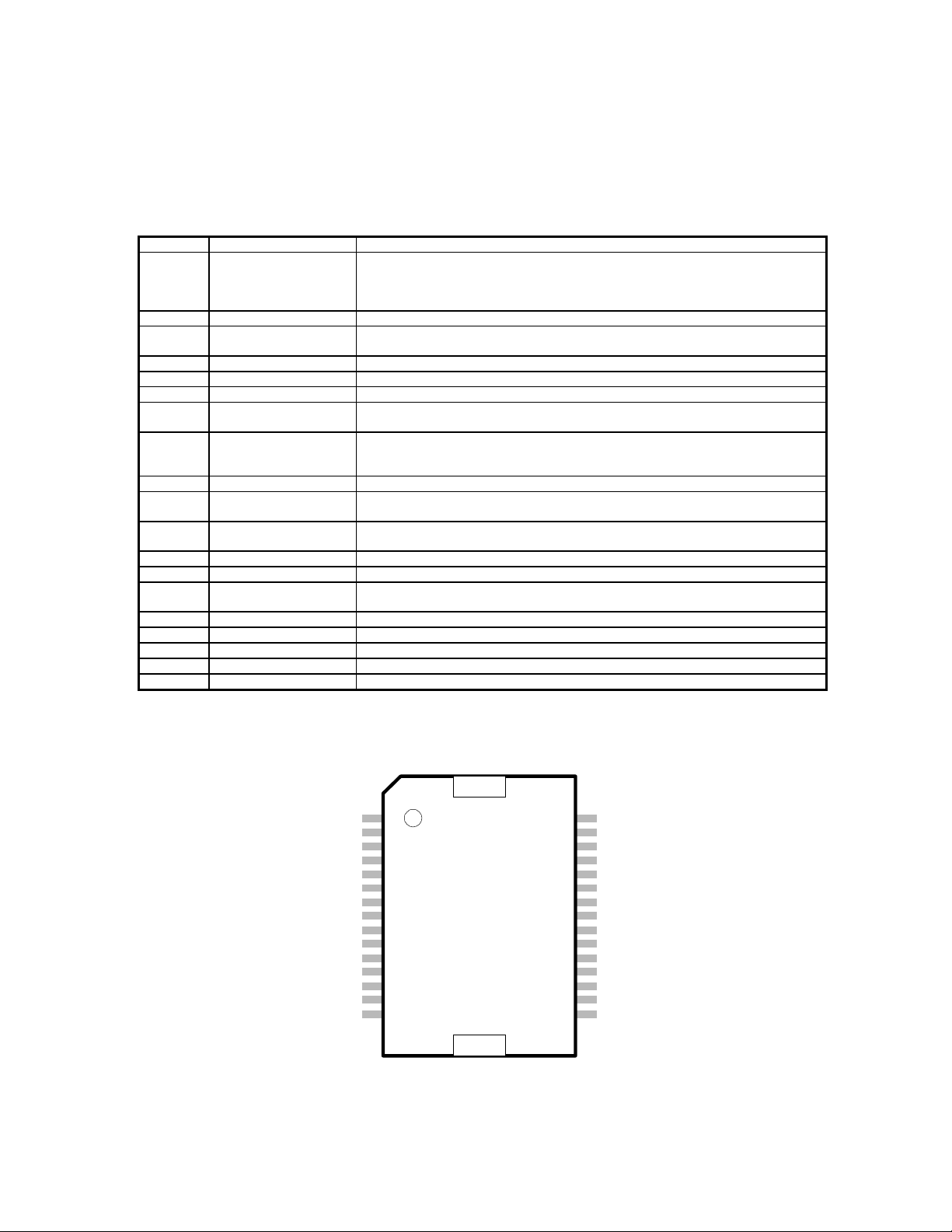
Pin Description
Pin
Function
1, 2 DCAP2, DCAP1 Charge pump switchi ng pi ns. DCAP1 (pin 2) is a free running 300kHz square
3, 8 V5D, V5A Digital 5VDC, Analog 5VDC
4, 7,
15
AGND1, AGND2,
AGND3
5 REF Internal reference voltage; approxim at el y 1.0 VDC.
6 OVERLOADB A logic low output indicates t he i nput signal has overloaded the ampl i f i er.
9, 12 VP1, VP2 I nput stage output pins.
10, 13 IN1, IN2 Single-ended inputs. Inputs are a “virtual” ground of an inverting opamp with
11 MUTE When set to l ogic high, both amplifiers are muted and in idle mode. When low
14 BIASCAP Input stage bias voltage (approximat el y 2. 4VDC).
16 SLEEP When set to logi c high, device goes into low power mode. I f not used, this pin
17 FAULT A logic hi gh out put indicates thermal overl oad, or an output is shorted to ground,
18, 28 PGND2, PGND1 Power Grounds (hi gh current)
19 DGND Digital Ground
20, 22;
25, 23
OUTP2 & OUTM2;
OUTP1 & OUTM1
21, 24 VDD2, VDD1 Supply pins f or hi gh current H-bridges, nominall y 12V DC.
26 NC Not connected
27 VDDA Analog 12VDC
29 CPUMP Charge pump output (nominally 10V above V DDA)
30 5VGEN Regulated 5VDC source us ed t o supply power to the input section (pins 3 and 8).
Description
wave between VDDA and DGND (12Vpp nominal). DCAP2 (pin 1) is level shifted
10 volts above DCAP1 (pin 2) with the same amplitude (12Vpp nom i nal ),
frequency, and phase as DCAP1.
Analog Ground
approximately 2.4VDC bias.
(grounded), both amplifiers are fully operational. If lef t floating, the device s tays in
the mute mode. Ground if not used.
should be grounded
or another output.
Bridged outputs
30-pin Power SOP Package
(Top View)
DCAP2
DCAP1
V5D
AGND1
REF
OVERLOADB
AGND2
V5A
VP1
IN1
MUTE
VP2
IN2
BIASCAP
AGND3
1
2
3
4
5
6
7
8
9
10
11
12
13
14
15
5VGEN
30
CPUMP
29
PGND1
28
VDDA
27
NC
26
OUTP1
25
VDD1
24
OUTM1
23
OUTM2
22
VDD2
21
OUTP2
20
DGND
19
PGND2
18
FAULT
17
SLEEP
16
TA1101B, Rev. 2.2, 08.17.00 3

TECHNICAL INFORMATION
Application / Test Circuit
4 TA1101B, Rev. 2.2, 08.17.00
 Loading...