

TRIPATH TDA2075A Technical data
现货库存、技术资料、百科信息、热点资讯,精彩尽在鼎好!
TDA2075A
Tripath Technology, Inc. - Technical Information
STEREO CLASS-T DIGITAL AUDIO AMPLIFIER DRIVER USING
TM
DIGITAL POWER PROCESSING
Preliminary Information Revision 0.9 – October 2005
GENERAL DESCRIPTION
The TDA2075A is a two-channel, amplifier driver, that uses Tripath’s proprietary Digital Power Processing
TM
(DPP
chipsets while providing exceptional audio performance for real world applications. Class-T amplifiers
offer both the audio fidelity of Class-AB and the power efficiency of Class-D amplifiers.
The TDA2075A is typically configured as a split-supply, single-ended, stereo amplifier. The TDA2075A
can also be configured single-supply, single-ended, stereo amplifier, via external component choice. For
applications that require bridged output drive, please refer to the TDA1400.
Applications
Powered DVD Players
Mini-Compo Systems
Audio/Video Amplifiers & Receivers
Multimedia Speakers
Benefits
Reduced system cost with smaller/less
Signal fidelity equal to high quality
High dynamic range compatible with digital
) technology. The TDA2075A offers higher integration over previous Tripath amplifiers driver
expensive power supply and heat sink
Class-AB amplifiers
media such as CD and DVD
TECHNOLOGY
Features
Class-T architecture with proprietary DPP
“Audiophile” Sound Quality
Full Audio Bandwidth, 20Hz to 20kHz
High Efficiency
Supports wide range of output power levels
and output loads by changing supply voltage
and external Mosfets
Compatible with unregulated power supplies
Output over-current protection
Over- and under-voltage protection
Over-temperature protection
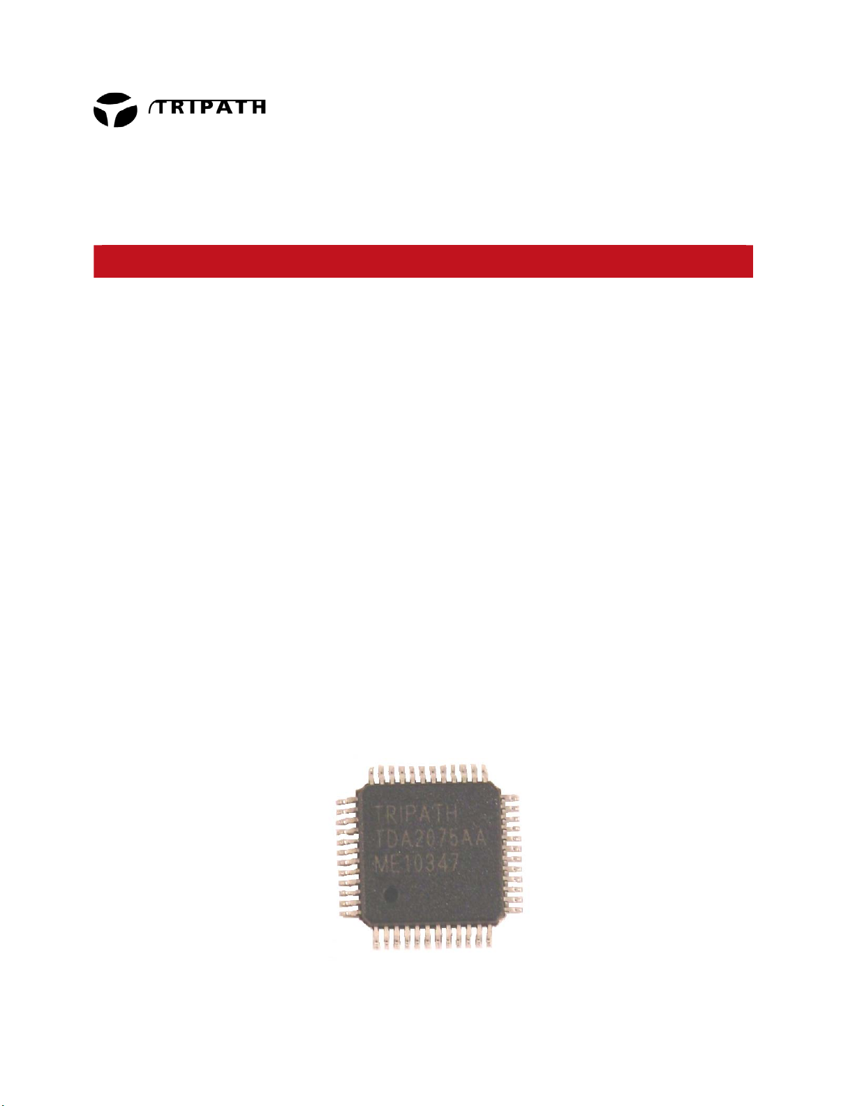
48-Pin LQFP Package
1 TDA2075A – Rev. 0.9/KLi/10.05

Tripath Technology, Inc. - Technical Information
Absolute Maximum Ratings (Note 1)
SYMBOL PARAMETER Value UNITS
V5 5V Power Supply 6 V
V
Input logic level V5 + 0.3 V
logic
V10
T
STORE
VPP, VNN Supply Voltage (Note 5) +/-70 V
T
A
TJ Junction Temperature 150º °C
ESDHB
ESDMM ESD Susceptibility – Machine Model (Note 3)
10V Power Supply 12 V
Storage Temperature Range -55º to 150º °C
Operating Free-air Temperature Range -40º to 85º °C
ESD Susceptibility – Human Body Model (Note 2)
All pins
All pins
2000
200
V
V
Note 1: Absolute Maximum Ratings indicate limits beyond which damage to the device may occur.
See the table below for Operating Conditions.
Note 2: Human body model, 100pF discharged through a 1.5KΩ resistor.
Note 3: Machine model, 220pF – 240pF discharged through all pins.
Operating Conditions (Note 4)
SYMBOL PARAMETER MIN. TYP. MAX. UNITS
V5
V10 10V Power Supply 9 10 11 V
T
A
VPP Positive Supply Voltage (note 5) 15 65 V
VNN Negative Supply Voltage (note 5) -15 -65 V
Note 4: Recommended Operating Conditions indicate conditions for which the device is functional.
Note 5: The supply limitation is based on the internal over-current detection circuit. This limitation is
5V Power Supply 4.5 5 5.5 V
Operating Temperature Range -40 25 85 °C
See Electrical Characteristics for guaranteed specific performance limits.
subject to additional characterization. In addition, depending on feedback configuration, the TDA2075A
can be used in single-supply applications, in which case, the negative supply, VNN, is not needed.
Thermal Characteristics
SYMBOL PARAMETER Value UNITS
θ
JA
Junction-to-ambient Thermal Resistance (still air) TBD C/W
2 TDA2075A – Rev. 0.9/KLi/10.05

Tripath Technology, Inc. - Technical Information
Electrical Characteristics TDA2075A (Note 6)
TA = 25 °C. See Application/Test Circuit on page 7. Unless otherwise noted, the supply voltages are
V5=5V, V10=10V, and VPP=|VNN|=40V.
SYMBOL PARAMETER CONDITIONS MIN. TYP. MAX. UNITS
I
5Q
I
10Q
I
VPPQ
I
VNNQ
I
5MUTE
V
TOC
I
VPPSENSE
V
VPPSENSE
I
VNNSENSE
V
VNNSENSE
Note 6: Minimum and maximum limits are guaranteed but may not be 100% tested.
Note 7: These supply voltages are calculated using the I
Quiescent Current
50 mA
(Mute = 0V)
Quiescent Current
(Mute = 0V)
Quiescent Current
(Mute = 0V)
Quiescent Current
(Mute = 0V)
Mute Supply Current
FETs: FQP13N10, FQP12P10
R
= 20.0kΩ
BBM
FETs: FQP13N10, FQP12P10
= 20.0kΩ
R
BBM
FETs: FQP13N10, FQP12P10
= 20.0kΩ
R
BBM
50
(Mute = 5V)
Over Current Sense Voltage
Threshold
+/-5V Common Mode Voltage
+/-40V Common Mode Voltage
VPPSENSE Threshold Currents Over-voltage turn on (muted)
Over-voltage turn off (mute off)
Under-voltage turn off (mute off)
Under-voltage turn on (muted)
Threshold Voltages with
= R
R
VPP1
VPP2
= 402KΩ
(Note 7)
Over-voltage turn on (muted)
Over-voltage turn off (mute off)
Under-voltage turn off (mute off)
Under-voltage turn on (muted)
VNNSENSE Threshold Currents Over-voltage turn on (muted)
Over-voltage turn off (mute off)
Under-voltage turn off (mute off)
Under-voltage turn on (muted)
Threshold Voltages with
= 402KΩ
R
VNN1
= 1.2MΩ
R
VNN2
(Note 7)
Over-voltage turn on (muted)
Over-voltage turn off (mute off)
Under-voltage turn off (mute off)
Under-voltage turn on (muted)
VPPSENSE
and I
Characteristics table. The typical voltage values shown are calculated using a R
60 mA
40 mA
40 mA
TBD
TBD
TBD
TBD
TBD
TBD
TBD
TBD
TBD
TBD
VNNSENSE
0.55
0.55
138
TBD
TBD
TBD
135
55
TBD
52
55.5
TBD
54.3
22.1
TBD
20.9
138
TBD
135
51
TBD
48
55.5
TBD
54.3
20.5
TBD
19.3
values shown in the Electrical
and R
VPP
mA
VNN
any tolerance variation. The minimum and maximum voltage limits shown include either a +1% or –1% (+1%
for Over-voltage turn on and Under-voltage turn off, -1% for Over-voltage turn off and Under-voltage turn on)
variation of R
VPP
or R
examples to show both typical and worst case voltage ranges for the given R
off the nominal 402kohm and 1.2Mohm values. These voltage specifications are
VNN
VPP
and R
VNN
Please refer to the Application Information section for a more detailed description of how to calculate the over
and under voltage trip voltages for a given resistor value.
V
A
µ
A
µ
A
µ
A
µ
V
V
V
V
A
µ
A
µ
A
µ
A
µ
V
V
V
V
values without
resistor values.
3 TDA2075A – Rev. 0.9/KLi/10.05

Tripath Technology, Inc. - Technical Information
Performance Characteristics
TA = 25 °C. Unless otherwise noted, the supply voltages are V5 = 5V, V10 = 10V, and VPP = |VNN| =
40V, the input frequency is 1kHz and the measurement bandwidth is 20kHz. See Application/Test Circuit.
SYMBOL PARAMETER CONDITIONS MIN. TYP. MAX. UNITS
P
Output Power
OUT
(continuous output)
THD + N Total Harmonic Distortion Plus
Noise
IHF-IM IHF Intermodulation Distortion
SNR Signal-to-Noise Ratio
η
Power Efficiency
AV Amplifier Gain
THD+N = 0.1%, R
THD+N = 1%, R
THD+N = 10%, R
THD+N = 0.1%, R
THD+N = 1%, R
THD+N = 10%, R
THD+N = 0.1%, R
THD+N = 1%, R
THD+N = 10%, R
= 60W, RL = 8Ω
P
OUT
= 4Ω
L
= 4Ω
L
= 4Ω
L
= 6Ω
L
= 6Ω
L
= 6Ω
L
= 8Ω
L
= 8Ω
L
= 8Ω
L
19kHz, 20kHz, 1:1 (IHF), R
P
= 25W/Channel
OUT
A Weighted, R
= 200W/Channel
P
OUT
P
= 115W/Channel, RL = 8Ω
OUT
P
= 10W/Channel, RL = 8Ω
OUT
= 4Ω,
L
= 8Ω
L
0.01 %
0.03 %
104.4 dB
92 %
20.09 V/V
See Application / Test Circuit
A
Channel to Channel Gain Error
VERROR
P
= 10W/Channel, RL = 8Ω
OUT
See Application / Test Circuit
e
Output Noise Voltage A-Weighted, input shorted
NOUT
R
FBC
= 10kΩ, R
= 1.1kΩ, and R
FBB
FBA
170
= 1.0kΩ
V
Output Offset Voltage No Load, Mute = Logic Low
OFFSET
1% R
FBA, RFBB
and R
FBC
resistors
-1.0 1.0 V
145
160
200
105
115
150
80
90
115
W
W
W
W
W
W
W
W
W
0.5 dB
V
µ
4 TDA2075A – Rev. 0.9/KLi/10.05
TDA2075A Pinout
Tripath Technology, Inc. - Technical Information
48-pin LQFP
(Top View)
NC
VNN SENSE
OVRLDB
VPPSENSE
AGND
AGND
OAOUT1
INV 1
MUTE
NC
OCD 1
OCD 2
REF
SUB
37
38
39
40
41
43
V5
44
V5
45
46
47
48
1
INV 2
DCMP
BIASCAP
OAOUT2
OCSP2
FAULT
NC
V5
30 29 27 2628 2536 35 33 3234 31
98765432
V5
AGND
BBMSET
GATEOFF
V10
FBOUT2
FBGND2
OCSN2
24
23
22
21
20
1942
18
17
16 NC
15
14
13
1110 12
OCSN1
OCSP1
FBGND1
FBOUT1
PGND
NC
HO2
NC
L02
NC
NC
LO1
HO1
NC
PGND
5 TDA2075A – Rev. 0.9/KLi/10.05

Tripath Technology, Inc. - Technical Information
Pin Description
Pin Function Description
1 OAOUT2 Output of inverting-input stage (Channel 2)
2 INV2 Negative input of inverting op-amp with 2.5VDC of bias (Channel 2)
3 BIASCAP Bandgap reference times two (typically 2.5VDC). Used to set the common
mode voltage for the input op amps. This pin is not capable of driving external
circuitry.
4 DCMP Internal mode selection. This pin must be connected to 0V or 5V for proper
device operation. Typically, this pin is connected to V5.
5 AGND Analog Ground
6 V5 5 Volt power supply input.
7 BBMSET Break-before-make timing control to prevent shoot-through in the output
MOSFETs. Please refer to the Application Information for additional
information.
8 GATEOFF 10V under-voltage fault pin (requires pull-up resistor)
9, 10 OCSP1, OCSN1 Over-current detect pins (Channel 1)
11 FBKGND1 Ground Kelvin feedback (Channel 1)
12 FBKOUT1 Negative switching feedback (Channel 1)
13 PGND Power Ground
15 HO1 High side gate drive output (Channel 1)
17 L01 Low side gate drive output (Channel 1)
20 LO2 Low side gate drive output (Channel 2)
22 HO2 High side gate drive output (Channel 2)
24 PGND Power Ground
25 V10 10 Volt power supply input. Used for gate drive circuitry.
26 FBKGND2 Ground Kelvin feedback (Channel 2)
27 FBKOUT2 Negative switching feedback (Channel 2)
28, 29 OCSN2, OCSP2 Over-current detect pins (Channel 2)
30 FAULT A logic high output indicates an under-voltage (5V or 10V), over-current or
over-temperature condition (requires pull-down resistor).
32 V5 5 Volt power supply input.
33 OCD2 Over-Current Detect pin (Channel 2). This pin must be connected to AGND for
proper device operation.
34 REF Internal bandgap reference voltage; approximately 1.0 VDC.
35 OCD1 Over-Current Detect pin (Channel 1). This pin must be connected to AGND
for proper device operation.
36 SUB Substrate (connect to AGND)
38 VNNSENSE Negative supply voltage sense input. This pin is used for both over and under
voltage sensing for the VNN supply.
39 OVRLDB A logic low output indicates the input signal has overloaded the amplifier.
40 VPPSENSE Positive supply voltage sense input. This pin is used for both over and under
voltage sensing for the VPP supply.
41 AGND Analog Ground
42 AGND Analog Ground
43 V5 5 Volt power supply input.
44 V5 5 Volt power supply input.
45 OAOUT1 Output of inverting-input stage (Channel 1)
46 INV1 Negative input of inverting op-amp with 2.5VDC of bias (Channel 1)
47 MUTE When set to logic high, both channels are in idle mode. When low (grounded),
both channels are fully operational (connect to FAULT pin).
14,16,18,
19,21,23,
31,37,48
NC Not Connected internally. These pins may be grounded or left floating on the
PCB layout.
6 TDA2075A – Rev. 0.9/KLi/10.05
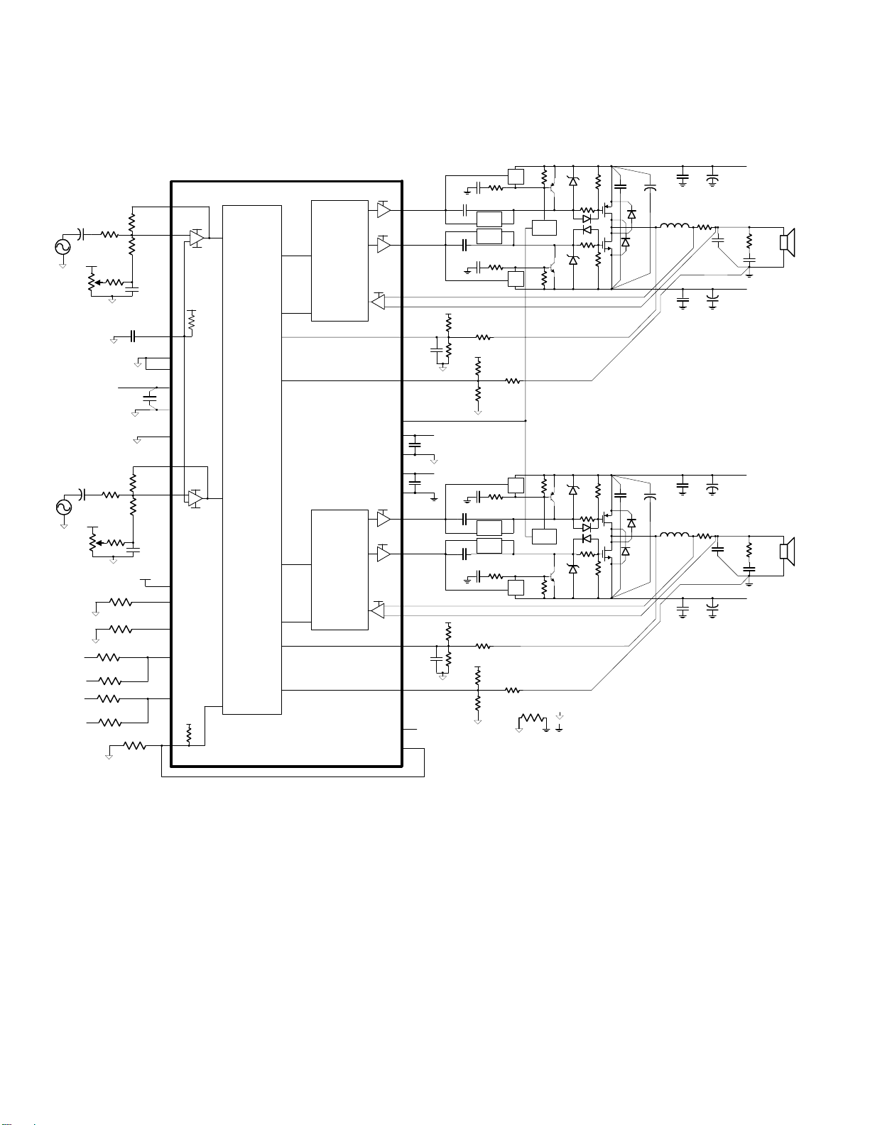
Application / Test Circuit
Tripath Technology, Inc. - Technical Information
C
2.2uF
R
50K
Offset Trim
Circuit
2.2uF
R
50K
Offset Trim
Circuit
VNN
VPP
**
TDA2075A
V5
V5
V10
V10
13,24
V10
V10
6, 32
15
HO1
LO1
17
OCSP1
9
OCSN1
10
FBKOUT1
12
FBKGND1
11
GATEOFF
8
V5
5
AGND
V10
25
PGND
22
HO2
20 LO2
OCSP2
29
OCSN2
28
FBKOUT2
27
FBKGND2
26
NC
FAULT
30
C
FB
150pF
C
FB
220pF
OAOUT1
45
I
R
R
I
F
20K
20K
+
V5
OFA
R
470K
R
OFB
470K
OFB
C
OF
0.1uF
AGND
C
A
0.1uF
BIASCAP
OCD2
OCD1
5V
C
S
0.1uF
AGND
OAOUT2
C
I
R
R
I
F
20K
20K
+
V5
OFA
V5
V5
R
470K
R
8.25K, 1%
R
*R
VNN1
*R
VNN2
*R
VPP1
*R
VPP2
OFB
AGND
REF
BBMSET
20K, 1%
R
OFB
470K
C
OF
V5
BBMSET
VNNSENSE
VPPSENSE
R
FLT
DCMP
MUTE
INV1
SUB
INV2
REF
V5
46
-
+
AGND
2.5V
FET controller
MUTE
3
33
35
V5
43, 44
41, 42
Processing
&
Modulation
36
1
V5
2
-
+
AGND
FET controller
4
34
7
MUTE
38
40
V5
14,16,18,19, 21, 23, 37, 48
47
10K
C
0.1uF
C
0.1uF
C
ISA
1.0uF
C
G
S_SUP
1.0uF
CKT
**
S_SUP
C
CKT
G
1.0uF
C
ISA
1.0uF
V5
R
*R
FBA
FBC
1K
10K, 1%
*R
FBB
V5
1.1K
R
1K
*R
5V
S
10V
S
C
ISA
1.0uF
C
G
S_SUP
1.0uF
CKT
**
S_SUP
C
CKT
G
1.0uF
C
ISA
1.0uF
V5
R
*R
FBA
FBC
1K
10K, 1%
*R
FBB
1.1K
V5
R
1K
*R
R
D_IS
ISA
D
BIAS
Q
ISP
D
BIAS
Q
ISN
D
BIAS
Q
ISP
D
BIAS
Q
ISN
Analog Ground
R
GS
C
150K
R
G
D
G
D
G
R
G
R
GS
150K
R
GS
150K
R
G
D
G
D
G
R
G
R
GS
150K
HBR
0.1uF
Q
P
D
Q
N
D
DS
C
HBR
0.1uF
Q
P
D
Q
N
D
DS
1.1K
1.1K
R
1.0K
R
1.0K
FBA
FBB
R
1.0K
R
1.0K
FBA
FBB
ISB
ISB
*R
10K, 1%
ISB
ISB
*R
10K, 1%
CKT
**
D_IS
CKT
FBC
**
D_IS
CKT
**
D_IS
CKT
FBC
4.7K
**
G_OFF
R
ISA
4.7K
R
ISA
4.7K
**
G_OFF
R
ISA
4.7K
Ω
0
CKT
CKT
Power Ground
* The values of these components must be adjusted based
on supply volt age range. See Applic ation Information.
** Refer to the RB- TDA2075A docume nt for a detailed
description of these optional circuits.
C
S
0.1uF
C
+
HBR
33uF
L
O
DS
11uH
R
S
C
S
0.1uF
C
S
0.1uF
C
+
HBR
33uF
L
L
O
O
DS
11uH
R
S
C
S
0.1uF
VPP
C
+
S
220uF
R
C
O
Z
R
0.22uF
10Ω,2W
C
Z
0.22uF
VNN
C
S
+
220uF
VPP
C
+
S
220uF
R
C
O
Z
0.22uF
10Ω,2W
C
Z
0.22uF
VNN
C
S
+
220uF
L
4 - 8Ω
R
L
4 - 8Ω
7 TDA2075A – Rev. 0.9/KLi/10.05

Tripath Technology, Inc. - Technical Information
External Components Description (Refer to the Application/Test Circuit)
Components Description
R
Inverting input resistance to provide AC gain in conjunction with RF. This input is
I
RF Feedback resistor to set AC gain in conjunction with RI. Please refer to the Amplifier
CI AC input coupling capacitor which, in conjunction with RI, forms a high-pass filter at
R
Feedback divider resistor connected to V5. This value of this resistor depends on
FBA
R
Feedback divider resistor connected to AGND. This value of this resistor depends
FBB
R
Feedback resistor connected from either the OUT1 (OUT2) to FBKOUT1
FBC
CFB Feedback delay capacitor that both lowers the idle switching frequency and filters
R
Potentiometer used to manually trim the DC offset on the output of the TDA2075A.
OFA
R
Resistor that limits the DC offset trim range and allows for precise adjustment.
OFB
COF Capacitor that filters the manual DC offset trim voltage.
R
Bias resistor. Locate close to pin 34 and ground to plane with a low impedance
REF
R
Bias current setting resistor for the BBM setting. Locate close to pin 7 and ground
BBMSET
CA BIASCAP decoupling capacitor. Locate close to pin 3 and ground to plane with a
CS Supply decoupling capacitor for the power pins. For optimum performance, these
R
Main overvoltage and undervoltage sense resistor for the negative supply (VNN).
VNN1
R
Secondary overvoltage and undervoltage sense resistor for the negative supply
VNN2
R
Main overvoltage and undervoltage sense resistor for the positive supply (VPP).
VPP1
R
Secondary overvoltage and undervoltage sense resistor for the positive supply
VPP2
biased at the BIASCAP voltage (approximately 2.5VDC).
Gain paragraph, in the Application Information section.
.
)CR2(1f
π=
IIC
the supply voltage setting and helps set the TDA2075A gain in conjunction with R
R
F, RFBA,
and R
. Please see the Modulator Feedback Design paragraphs in the
FBC
I,
Application Information Section.
on the supply voltage setting and helps set the TDA2075A gain in conjunction with
R
I, RF, RFBA,
and R
. Please see the Modulator Feedback Design paragraphs in
FBC
the Application Information Section.
(FBKOUT2) or PGND1 (PGND2) to FBKGND1 (FBKGND2). The value of this
resistor depends on the supply voltage setting and helps set the TDA2075A gain in
conjunction with R
I, RF, RFBA,
power rating of greater than
, and R
=
DISS
. It should be noted that R
FBB
2
. Please see the Modulator
)(2RVPPP FBC
must have a
FBC
Feedback Design paragraphs in the Application Information Section.
very high frequency noise from the feedback signal, which improves amplifier
performance. The value of C
should be different for channel 1 and channel 2 to
FB
minimize noise coupling between the channels. Please refer to the Application /
Test Circuit.
connection to pins 41 and 42.
directly to pin 5. See Application Information on how to determine the value for
R
.
BBM
low impedance connection to pins 41 and 42.
components should be located close to the TDA2075A and returned to their
respective ground as shown in the Application Circuit.
Please refer to the Electrical Characteristics Section for the trip points as well as the
hysteresis band. Also, please refer to the Over / Under-voltage Protection section in
the Application Information for a detailed discussion of the internal circuit operation
and external component selection. When using a single power supply, this circuit
can be defeated by connecting a 16KΩ resistor to AGND.
(VNN). This resistor accounts for the internal V
resistor value should be three times that of R
VNN1
NNSENSE
bias of 1.25V. Nominal
. Please refer to the Over / Undervoltage Protection section in the Application Information for a detailed discussion of
the internal circuit operation and external component selection. When using a single
power supply, omit R
VNN2
.
Please refer to the Electrical Characteristics Section for the trip points as well as the
hysteresis band. Also, please refer to the Over / Under-voltage Protection section in
the Application Information for a detailed discussion of the internal circuit operation
and external component selection.
8 TDA2075A – Rev. 0.9/KLi/10.05
 Loading...