

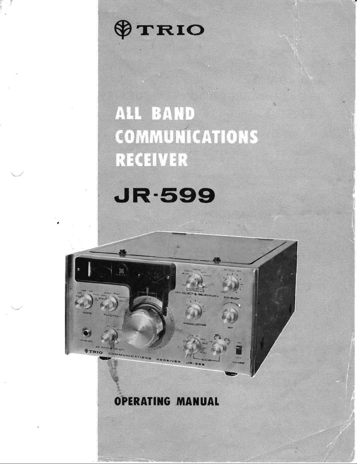
Trio JR-599 User Manual
'",
JR-589
~TR.IO
ALL
SSB
BAND
COMMUNICATIONS
~R-599
(I)
The
model
models:
SPECIAL (M)
These models may be identified
plates
The
attached
major
showninthe
Model
CUSTOM
CUSTOM SPECIAL
CUSTOM SPECIAL
DELUXE
JR-599
CUSTOM
and
CUSTOM SPECIAL (X).
on
the
differences
table
below.
SSB,
SSB, FM,
(M)
SSB, FM, CW,
(X)
is
front
IF
FM
classified
DELUXE,
by
panels.
of
these models are
Filter
CW,
AM
AM
VHF
Not
144 MHz
50
into
three
CUSTOM
their
name
Converter
equipped
converter
& 144 MHz
converter
RECEIVER
(2)
Optional
availableatdealersofour
modify'
CUSTOM
SPECIAL
as
We
with a
this
filters
and
sub-models CUSTOM
SPECIAL
(X) by
are sure
smart
that
their
users
and
manual.
crystal
converters
products
(M)
into
models
own
hands.
can
entertain
pleasant QSO
are
for users
DELUXE
CUSTOM
themselves
after
reading
made
to
and
11111
1111111I11111I1'·1111
Special
Circuit Description : . . . . . . . .
Controls and their Functions : . . . .
Operating Instructions . . . . . . . . . . . . . . . . . . . . . . . . . . . . . . . . . . . . . . . . . . . . .
Accessory Circuitry 22
Alignment :
Maintenance 27
Schematic Diagram 29
Specifications . . . . . . . . . . . . . . . . . . . . . . . . . . . . . . . . . . . . . . . . . . . . . . . . . . . .
II
'Ir!UIIIIIIW"III(JHlI IIItI1Illftfl
1111I11
ltllll
l/IllllIlllllllIlllll/lIIl1l1llllllU
Iltlllli:lllllllll!llllllllllllllllllllJllllllllllllrtlllllllllllHtllltlUlIIllItIIlI
Features....................................................
tllllllllllllll!lIIll11IIl11JllttlllTllllln
..
..
10
..
15
..
25
..
30
Htlll..ltlIIIIIIIJUtItIIllIIlI
2
3
Iltl
CONTENTS
1111:1
'Ill I lflll"
1
SPECIAL
Qllmllllllllllllllllllllllllllllllllllllllllllllllllllllllllllllllllllllllllllllllllllllllllllllllllllllllllllllllll1I11111l11111111l11l111111111111111111111111111111111111111111111111l1111111111111111111111111111111111111111111111111111lI111111111l1111111111111l11111111111111l11111111111111111111111111111111111111111111111l11111111l1111
1.
All solid
receptionofthe
freq
uency
and
standard
2.
Field
amplifier
and
tu
be receivers characteristics.
3. IC
4.
employed
stability
VFO
low noise-factor
5. Precision
variable
provided for main
kHz
receiving frequency readable
Hz.
Fixed
6.
channels-spot
frequencies.
7. Amplifier
selector
high
for SSB signal.
8.
100
circuits
calibration available for every
turn
this
~SO.
9. Receiver incremental
corporated
of
receiving frequencyorcorrectionofa
frequency
ing dial during a
operation,
mitter.
state
range from 1.8to29.7
144 MHz
signal.
Effect
and
image characteristics
and
employing
type
capacitor
band
channel oscillators self-contained for 5
type
switch - distortionless
input
and
25
incorporated
of
main
set
as a frequency measuring set during
circuits insure high
amateur
bands
Transistor
mixer - a SIN, cross
as
IF
gain.
FET
output.
double
with
its
reception
AGC circuit
signal, whichisspecifically useful
kHz
tuning
provides
without
combined
as practised using a
bands
allocated over a
and
WWV's 10 MHz
(FET)
better
amplifier provides lligh
provides a highly-stable,
gear mechanism
with
linear characteristic
tuning
one
crystal
means
manipulation
dial covering a 25
complete
to
the
available for 5 specific
with
receptionofa
controlled
- precise frequency
one
.dial as well as for use
tuning
(RIT)
for fme
transmitter-receiver
quality
MHz,
used as
modulation
than
vacuum
....
turn
nearest
time-constant
calibrator
complete
circuit in-
adjustment
of
main tun-
mated
the
and
- a
500
tuned
trans-
FEATURES
and
and
FM
positiontointerlock
the
MODE switch.
incorporated
- for
controlofcrystals for
attenuator
provide
40
switch -
transformerless (OTL)
distortion
combined
TX-599
extremely high-degree transmi Her-receiver
are
controlofthe
50
RF
of
11. Crystal
SSB
selected as desired by means
depending
ference with a SELECTIVITY
AUTO
with
filter
CIAL
12. Beat frequency oscillator (BFO)
under
receptions with an electronic switch provided
for selection
RF
13.
to
0, 20,
selector
serve as a field
14.
Output
frequency
with low
15.
Operable
source as well as a DC 12 V source, as selected
by means
16. Provision
MHz crystal converters. [Model
CIAL (M) self-contains a 144 MHz
and Model CUSTOM SPECIAL (X)
and 144 MHz converter.]
17. A
available when
model
transmitter
18.
An
operation,orthe
is practicable when a
JR-599
mitter
under
LC filters serving asIFfilters for
receptions
on
the
AM
reception."
ofanappropriate
insertedinantenna
means
and
circuit
from an AC 100, 117,
of
is
Receiver
for
60
strength
adopted
a voltage
made for
transmitter-receiver
operated
Transmitter,
for
model
so-called cross-operated
operated
respectively, are easily
of
a MODE switch
condition
"An
in model CUSTOM SPE-
adjustmentofRF
dB
steps, as selected using a
enables·
measuring set.
factor
selector
mountinga50
JR-599
combination
and
Model
with their VFOs placed
mated
of
radio inter-
switch
its
electron
additional crystal
both
SSB
crystal.
input
model
- high
available.
in
conjunction
sets.
JR-599
type
power
220or240
switch.
CUST9M
a
combination
Receiver.
TX-599
placed in
operated
converter
operation
of
switch
and
CW
circuit
gain
by
to
audio
output
and 144
SPE-
both
50
with
VFO,
model
Trans-
V
10. Ring, linear
SSB,
AM
and
and
ratio
FM signal
detectors
receptions
equipped
respectively.
for
19.
Communication
abletoinsure higher-quality reception.
speaker
"SP-55"
made
avail-
2
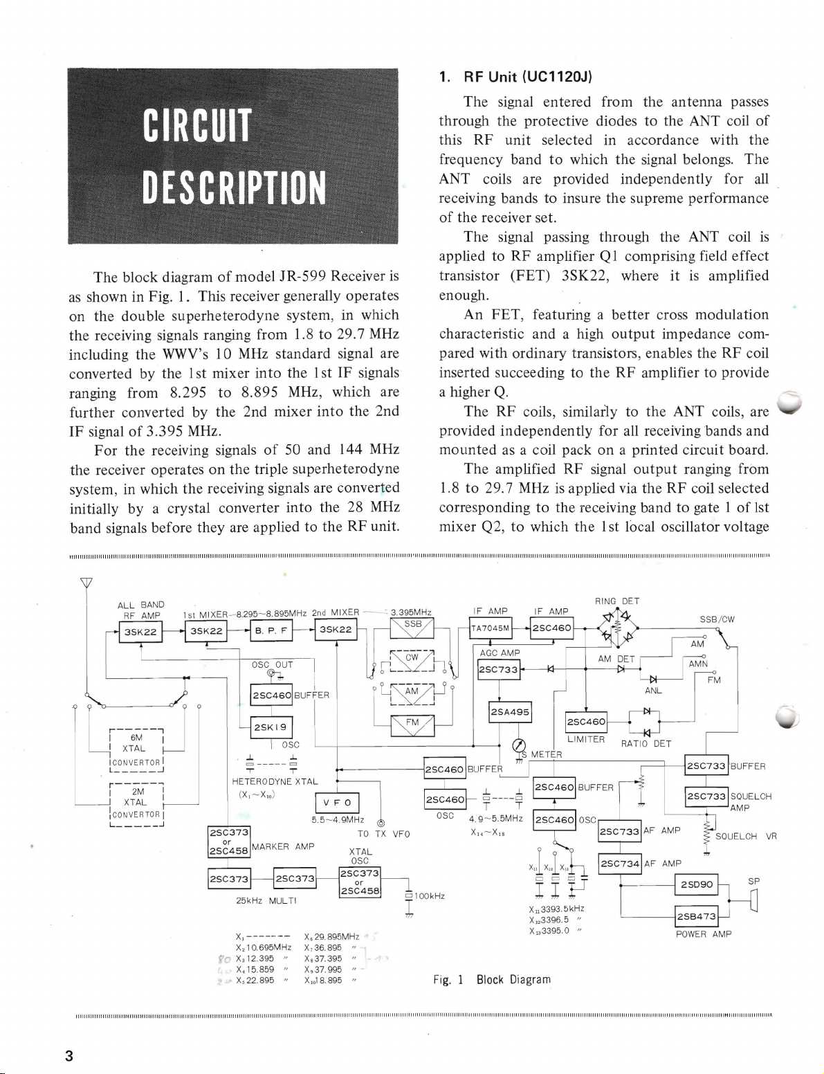
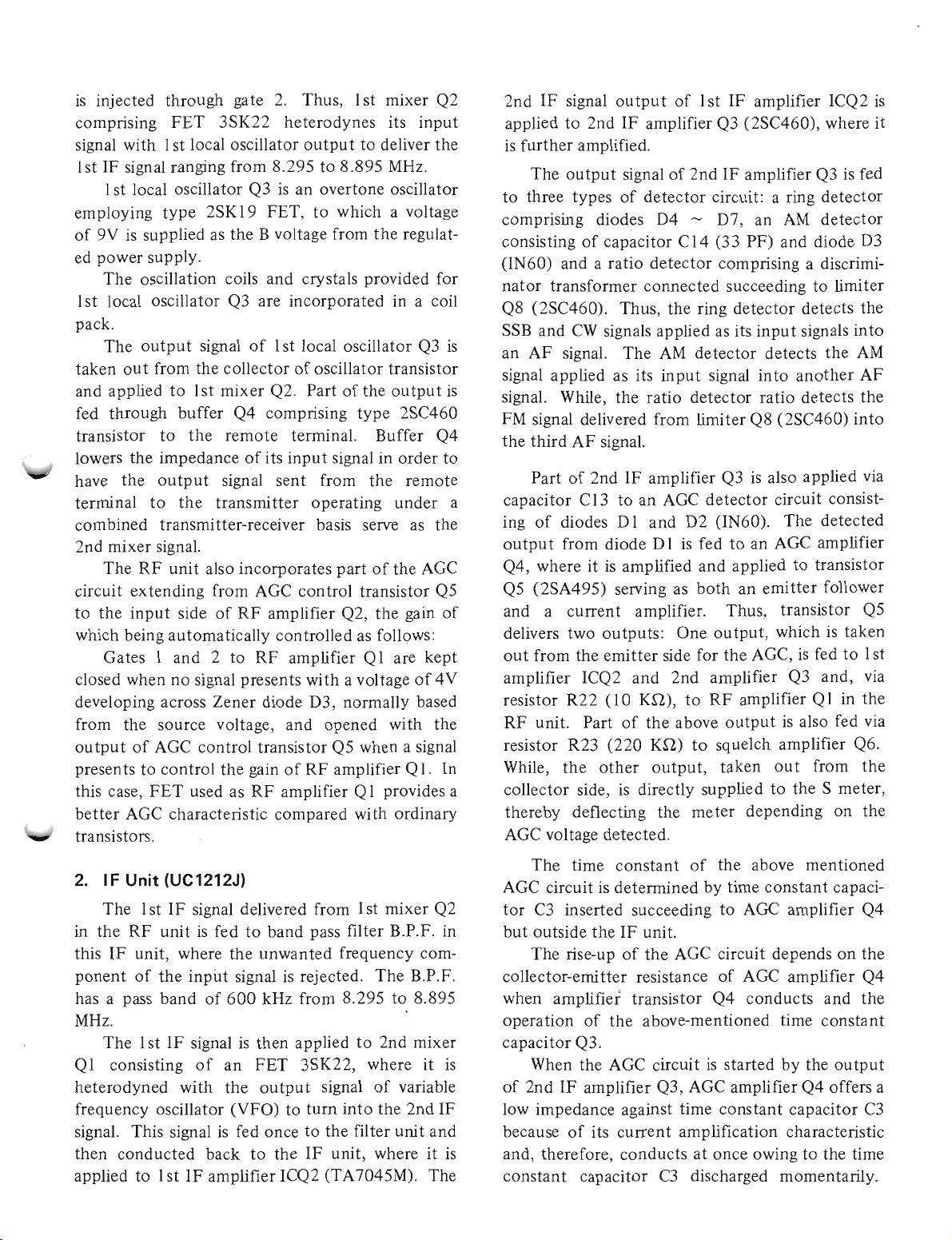
The block diagramofmodel JR-599 Receiver
as
showninFig. 1. This receiver generally operates
on
the
double
the
receiving signals ranging from 1.8to29.7
including the WWV's 10
converted by the 1st mixer
ranging from 8.295
further converted by the 2nd mixer
IF
signalof3.395 MHz.
For
the
the receiver operatesonthe
superheterodyne
MHz
to
8.895 MHz, which are
receiving signals
system, in which
MHz
standard signal are
into
the 1stIFsignals
into
the 2nd
of
50 and 144
MHz
triple superheterodyne
system, in which the receiving signals are converted
by
initially
a crystal converter
band signals before they are applied
into
the 28 MHz
to
the
RF
unit.
1.
RF Unit (UC1120J)
The
signal entered from the
through the protective diodes to the ANT coil
this
RF
unit selected
frequency band
to
in
accordance with the
which the signal belongs.
ANT coils are provided independently for
antenna
passes
of
The
all
receiving bands to insure the supreme performance
of
the receiver set.
The
signal passing through the ANT coil
applied to
is
transistor
RF
amplifier Q1 comprising field effect
(FET)
3SK22, where
it
is
amplified
is
enough.
An FET, featuring a
characteristic and a high
pared with ordinary transistors, enables the
inserted succeeding to
a higher
The
Q.
RF
coils, similady to
the
better
output
cross modulation
impedance com-
RF
amplifier to provide
the
ANT coils, are
RF
coil
provided independen tly for all receiving bands and
mounted
1.8
corresponding
as a coil pack
The
amplified
to
29.7 MHzisapplied via
RF
to
the receiving bandtogate 1of1st
on
a printed circuit board.
signal
output
the
ranging frbm
RF
coil selected
mixer Q2,towhich the 1st local oscillator voltage
111111111111111111111111111111111111111111111111111111111111111111111111l1l11l11l11111111111111111111111111ll111111111111111111l111111111l11l1Illllllllll1111111111111'1l11111111111111l1111111111IlJllllllJll11111l1J1111l111111l1111l11111111111111111l111l1111l1111111l111lIllllllllllllllll1JllllllllllllllllllllllllllllllllllJllllllll1flllll
RING
DET
AM
OSC
r
C>-r
__
6M
__
~-'J
WXTAL U
ICONVERTORI
L
r-----~
I
:CONVERTOR
L
2M
XTAL I
...J
I
I
...1
OUTI
~I
l.-...,....--J
~BUF~ER
r
I
OSC
...I. .J.
=
-----
O.695MHz
=
5.5-4.9MHz
X,
29.
X,36.895
X.37.395 "
X,37.995 "
X,,18.895 "
t--
895MHz
__
~BUFFER
r:::::::::::L
~
OSC
TOTXVFO
"
Fig.
4.9-55MHz
Block
1
T T
HETERODYNE XTAL
(X,-X,,)
Xl
-------
X,l
S'r
X,12.395 "
X,15.859 "
X,22.895 "
1----l<:l-f-+-_-jD)l-E_T~
L{>I-J
.1.
.L
=r----T
Xn3393.5kHz
X,,3396.5
X,,3395.0 "
Diagram
"
ANL
~
POWER
FM
VR
AMP
IlllllllllI11111111l11111111111lllll1rllllllllllllllllllllll1111111111111111111111111111111111111111111111111111111111111111111111111:11111111111111111111111111111111111111111111111111111111111111111111111111111111111111111111111111111111111111111111111111111111111111111111111111111111111111111IIIIIIIII1IlllllltlNIlIIIIIIIIIIIII1ll111
3
is
injected
comprising
signal with I st local oscillator
1st IF signal ranging from
Ist local oscillator Q3
employing
of
9Vissupplied as
power
ed
The
1
st
local oscillator Q3 are
throughgate
FET
type
3SK22
2SKl9
2.
heterodynes
8.295to8.895
is
an
FET,
the
B voltage from
Thus, 1st
outputto
overtone
to
which a voltage
the
mixer
its
input
deliver
MHz.
oscillator
regulat-
Q2
the
supply.
oscillation coils and crystals provided for
incorporated
in a coil
pack.
The
output
taken
out
and applied
fed
through
transistor
lowers the
the
have
terminal
to
combined
2nd
mixer
The
RF
circuit
to
the
extending
input
which being
Gates1and
signal
from
the
to
1st
buffer
to
the
impedanceofits
output
the
of
1st local oscillator Q3
collectorofoscillator transistor
mixer
signal sent from
transmitter
Q2. Partofthe
Q4 comprising
remote
terminal.
input
operating
type
Buffer
signal in
the
output
2SC460
order
remote
under
transmitter-receiver basis serve as the
signal.
unit
also
incorporates
from AGC
side
of
RF
automatically
2 to
RF
amplifier Q2,
controlled
amplifier
partofthe
control
transistor
the
gain
as follows:
Ql
are
AGC
kept
Q4
to
Q5
of
closed whennosignal presents with a voltageof4V
developing across Zener diode D3, normally based
from the source voltage, and
outputofAGC
presents
this case,
better
to
FET
AGC characteristic
control
control
used as
transistor Q5 when a signal
the
gainofRF
RF
amplifier Q1 provides a
compared
opened
amplifier Q1.In
with the
with ordinary
transistors.
2nd
IF
signal ou
appliedto2ndIFamplifier Q3 (2SC460), where
is
further
to
three
The
amplified.
output
types
comprising diodes D4
consistingofcapacitor
(IN60) and a
nator
transformer
Q8 (2SC460). Thus,
AF
CW
signal.
is
an
SSB and
signal applied as its
is
a
signal. While,
FM
signal delivered from limiter Q8 (2SC460)
the
third
AF
Part
of
capacitor
ing
output
Q4, where
Q5
and a
Cl3
of
diodes D 1
from
itisamplified
(2SA495)
current
delivers two
out
from
the
amplifier ICQ2
resistor
RF
R22
unit. Part
resistor R23
While,
collector
thereby
the
side,isdirectly suppliedtothe S meter,
deflecting the
AGC voltage
tputof1st
IF amplifier ICQ2
signalof2ndIFamplifier Q3 is fed
of
detector
circuit: a ring
~
D7, an
AM
detector
detector
C14 (33 PF) and diode D3
ratio
detector
connected
the
signals applied as its inpu t signals
The
AM
input
the
ratio
comprising a discrimi-
succeedingtolimiter
ring
detector
detector
signal
detector
detects
into
ratio
detects
another
detects
the
the
into
AM
AF
the
into
signal.
2ndIFamplifier Q3isalso applied via
to
an AGC
and
diode
D1isfedtoan AGC amplifier
serving as
detector
circuit consist-
D2 (IN60).
and
appliedtotransistor
both
an
emitter
The
detected
follower
amplifier. Thus, transistor Q5
outputs:
emitter
(l0
of
(220
other
and
K.Q),
the
K.Q)
One
side for
2nd
to
above
output,
output,
the
which is taken
AGC,isfedto1st
amplifier Q3
RF
amplifier Q 1 in
outputisalso fed via
to
squelch amplifier Q6.
taken
meter
out
depending
from
and,
on
via
the
the
the
detected.
is
it
2.
IF Unit (UC1212J)
The
in
the
RF
this
IF
unit, where
ponent
of
has a pass
1stIFsignal delivered from 1st
unitisfedtoband pass filter B.P.F. in
the
unwanted
the
input
signalisrejected.
bandof600
kHz from
mixer
frequency com-
The
8.295to8.895
MHz. .
The1stIFsignalisthen
Ql
consisting
heterodyned
of
with
an
the
frequency oscillator (VFO)
signal. This signal
then
conducted
applied to 1stIF
is
fed oncetothe
back
amplifier ICQ2 (TA 7045M).
appliedto2nd
FET
3SK22, where
output
to
to
the
signal
turn
into
of
the
filter
IF
unit, whereitis
unit
Q2
B.P.F.
mixer
it
variable
2nd
IF
and
The
The
time
constant
AGC circuit is
tor
C3
inserted succeedingtoAGC amplifier Q4
but
outside
The
rise-upofthe
determined
theIFunit.
collector-emitter resistance
when amplifier transistor
operation
capacitor
is
When the AGC circuit
of
2ndIFamplifier Q3, AGC amplifierQ4offers a
of
Q3.
the
low impedance against time
because
and, therefore,
constant
of
its
capacitor
current
conductsatonce
of
the above
by time
mentioned
constant
AGC circuit dependsonthe
of
AGC amplifier Q4
Q4
conducts
above-mentioned time
is
startedbythe
constant
capacitor
amplification characteristic
owingtothe time
C3
discharged momentarily.
capaci-
and
the
constant
output
C3
When
the
impedance against time
thereby bringing itself
slowly becauseofcapacitor
Thus,
the
outputof2nd
IF amplifieriscut
off, on
contrary, AGC amplifier Q4 increases its
it
follows
constant
to
the
C3
that
AGC amplifierQ4provides an
capacitor C3,
cut-off
condition
charged gradually.
ideal quick-start slow-release characteristic for its
operation.
operation
switch
the
quick AGC operation.
position
(Note
applies to a case where the FUNCTION
is
placed in
of
FUNCTION switch AGC amplifier
provides an AGC characteristic
above characteristic because
of
charge
time
that
the
constant
the
above-mentioned AGC
(AGC)
For
of
FAST
just
position for
the
(AGC) SLOW
oppositetothe
the
discharge and
capacitor C3
Q4
conducted
reversely.)
the
way,
the
By
outputofAGC transistor Q5
applied via resistor R23 to squelch amplifier Q6
is
(2SC733)
base
controlling
amplified there and
of
buffer transistor Q7 (2SC733),
the
base voltage with
As a result, buffer transistor Q7 controls
amplifier
perform a squelch
Ql
in the
AF
operation
then
appliedtothe
the
unit with its
under
controlofthe
input
output
thereby
signal.
AF
inpu t signal.
Buffer transistor Q7,
an
acts as
impedance
or
FM signal with a lower impedance
emitter
to
conduct
volume control outside the
the
MODE switch from
mentioned
follower providing a higher
the
detected
IF
the
2nd
unit,asselected by
above, also
SSB,
to
IF
amplifier Q3
CW,
the
AM
AF
output.
3.
Filter Unit (UC1213J)
The
filter
unit
is inserted outside
the
between
of
1stIFamplifier Q2 in
This
outputof2nd
unit
incorporates four fllters with diode
switches provided for
signals respectively. These
thatanappropriate
filterisselected by meansofa
mixer
the
latter
the
SSB,
CW,
filters are so designed
diode switch when the MODE switch
Q2 and
unit.
AM
the
IF
the
and FM
is
placed in
unit
input
the position for a desired receiving signal.
that
the
Now, suppose
the
in
SSB position for reception
signal. This applies a voltage
the
terminal for
causes a
currenttoflow from the terminal through
resistor RI
resistors R2 (4.7
diode switchoffilter
(220
D)
kD)
MODE switchisplaced
of
of
13.8 Vtothe SSB
in
the
two directions to
and R3
(220
D).
the SSB
XF-l.
This
Thus, the
to
current passing resistor R2 flows
current
(1
resistor R3 flows as
resistor
R22
tion a positive voltage
kD)
(1
through
to
R4
diode D 1(lN60) and resistor R21
the
earth. While, the
(4.7
kD),
kD)tothe
the
diode D2
earth.
of
forward
Under
approx. 2.3 Visbuilt
as
current
current
(lN60)
the
the
forward
passing
through
and resistor
above condi-
up across resistors R21 and R22 to the earth. This
to
applies a backward voltage
(l
N60). As a result, diodes D 1 and D2 turns
D8
ON and diodes D3
allowing only
XF-l
from 2nd
The ratio
OFF
The
of
4.7
Hence,
DC
resistance
of
the
mH),
of
conditionsofthe
XF-l
kD
and an external capacitanceof33 pF.
the
filter is so designed
resistors for diode switch as
of
printed
the
capacitanceoflead wires and
capacitance as
Other
filters for
through
the
SSB signaltopass
mixer
the
Q1to1stIFamplifier Q2.
signals
under
diodesisapprox.70dB.
filter requiresanexternal resistance
4.7
kD
and
circuit board and coilsL1and L2
the
external capacitanceof33 pF.
the
diodes D3 through
D8 turns
OFF,
through
the above ON and
thatitemploys the
the
the
internal capacitances
other
CW,
AM
and FM signals
thereby
fllter
external
stray
XF-2, XF-3 and a LC circuit are selected by their
diode switches
ed above when
CW,
AM
and FM positions, respectively.
4.
VFO
The
VFO
justinthe
the
Unit (UC0116J)
Unit
incorporates a variable frequen-
cy oscillator circuit, which delivers
same
manner
as describ-
MODE switch is placed in
the
output
the
frequencies varied over a frequency rangeof600
kHz from 5.5 to 4.9 MHz
order
to convert
the
l.st
8.895 to 8.295 MHz
into
to
the
2nd
IF
signals ranging from
the
2nd
IF
mixer in
signal
of
3.395 MHz.
A sub-dial scale is calibrated for
frequency range from graduation 0
the
to
gradation
above
600atintervalsof1 kHz.
The
variable frequency osicllator consists
oscillator transistor Q1 (3SK22) arranged
modified Clapp socillator circuit and
stably with
The
output
buffer
transistor Q2
of
variable frequency oscillator
operate
(2SKI9).
of
as
quite
deliversed through buffer transistor Q2 and one
of
stage
harmomic filter to
the
output
circuit, a
Darlington circuit comprising amplifier transistors
Q3 and Q4, Hence, the
the
stably against
variationofits load.
output
circuit operate
(l
a
is
5
The
YFO
incremen
voltage
The
tal
RIT
generated
incorporatedinthe
a receiver relay during
combined
the
YFO
YFO
SELECT
panel provides
mentioned
Note
removed
its
from
adjustment
unit
also
incorporates
tuning
(RIT)
circuit
in its
circuit.
is
operated
generator
UC I0 IOJUnit
the
transmitter-receiver
frequency
dial.
RIT
voltage.
that
means
the
regardless
The
RIT
for
YFO
Unit
controlling
its caseormodified
needs a high degreeofadjustment
technique.
5.
Carrier (BFO)
The
carrier
oscillator
transistor
(2SC460)
The
(BFO)
BFO
Q2
and crystals
diode switch consisting
(I
SI555),
ring
inserts a
detector
Unit
(UC1214J)
unit
incorporates
circuit.
circuit, consisting mainlyofoscillator
(2SC460),
X-I,
of
diodes DI
beatorcarrier
for
reception
signal.
output
capaci
transistor
frequencies are
Oscillator
and its
of
trimmer
parallel with crystal X I
Q2isthe
torsTCI
through
through
Selectionofa crystal for
of
the
CW,
LSBorUSB signalisperformed
above-mentioned
Suppose,
placedinthe
signal. This applies a
Y
to
the
LSB
diode
switch as follows:
for
example,
LSB
position
power
terminalofthe
that
for
As a result, a forward voltage
LSB
terminal
choke
internal
This in
conducting
by
with
the
base
and
coil
resistance
turn
Hence, oscillator
at
the
X3 crystal
The
beat
the
same
of
the
USBorCW
through
resistor
L4(ImH)todiode
the
diode
since
becauseofthe
inserts crystal
diode
via
capacitor
emitter
of
oscillator
transistor
frequency,or3393.5
frequency
oscillator
mannerasmentioned
signal. But, its
X3
Q I
a receive
from
the
circuit, which
and
actuated
reception
operation,
of
control
the
under
and
setting
on
the
the
should
never be
internally
a beat
buffer
X-2
frequency
transistor Q2
and
X-3
with
through
frequencyinthe
of
the
SSB
or
Pierce B-E circuit
adjusted
by
TC3 inserted in
X3 respectively.
the
BFO in
reception
by the
the
MODE
switch
receptionofa LSB
supply
voltageof13.8
Carrier (BFO) Unit.
is
applied from
R4
(22
kS1)
D4(IS1555), there-
the
diode
offers
voltage applied.
connected
C6
(22
pF)
in series
across
transistor
starts
in oscillation
kHz.
operates
above
center
for
reception
frequency
just
RIT
by
the
varies
of
front
above-
since
D4
CW
means
the
and
a low
the
Q
I.
in
3.395
reception
frequency
is
IF
the
makesitdifficulttoreceive
MHz
is
shifted
of
the
zero beats
CW
by
700
to
signal because the
with
theoutput
800
Hz
signalof2nd
amplifier Q3 in this case owingtothe fact
output
signal'iscontinuous
the
wave,
incoming
and
frequen-
for
center
that
this
cy.
The
above-mentioned
is
accomplished
cy
When
position,
terminal
kS1)
turning
through
therefore,
and emi
oscillator
frequency
cy.
adjusted
TC
a
I, which provides
the
MODE
a DC voltageisapplied
of
this carrier
and
choke
the
the
insert
coil
diode
diode
the
tterofoscilla
transistor
The
a little
beat
lower
tone
through
frequencyby±200
The
output
of
by
shiftofthe
the
diode
YFO
switch
frequen-
as follows:
switchisplacedinthe
from
the
CWR
unit
Ll
(I
ON. This
without
via resistor
mH)
grounds
any
capacitor
to
diode
crystal X2
RI
crystal directly across the base
tor
for
the
Q2
the
use
means
transistor
starts
than
Q I. As a result, .
in oscillation at a
the crystal frequen-
CW
reception
of
trimmer
for
varying the BFO
may
capacitor
Hz.
BFO
oscillator
transistor
Q I
CW
(2.2
D I,
and,
be
is
applied via a voltage divider circuit comprising
capacitor
transistor Q2.
emitter
low as a
of
the
6.
The
is
rates a
generates a
from
for
of
accomplished
The
mainly
(2SC373)
TransistorQ1,
,«ith
kHz.
collector
means for fine
CII
(10
Buffer
follower, offers an
bout
100
output
25 kHz / 100
voltage
25
kHz/100
marker
marker
3.5to28
calibration
a
25
MHzatintervalsof25or100
of
or
100
by
marker
of
four
and
one
the100
kHz
Trimmer
circuitofoscilla
pF)
and
transistor
S1,
thereby
and
frequency.
kHz
Marker
kHz
signal
generator
signal over a
the
main
kHz
marker
meansofthe
signal
generator
transistors Q I
100
kHz
actingasan
crystalata
capacitor
tor
adjustment
CI3
(22
pF)tobuffer
Q2,
acting
output
impedance
minimizing variation
Unit
(UC1505J)
marker
unit
incorpo-
circuit which
frequency
tuning
dial. Selection
signal
may
FUNCTION
circuit
consists
through
crystal
(HC/!3U).
oscillator, oscillates
frequency
TCIinserted
transistor
of
the
Q I provides
oscillator fre-
as an
range
kHz
be
switch.
Q4
of
100
in ,the
as
quency.
The
capacitor
outputofoscillator
C4
(33
pF)todiode
transistor
D I,
Q Iisfed via
through
which
6
itisshaped
period
free-running multivibrator consisti.ng
Q2 and Q3 at a period
multivibrator has a free-running period
of
into
one
a pulsed wavefonn occuringata
fourth
the
100 kHz and drives a
of
of
just
25
kHz since the
of
transistors
about
25
kHz.
The
output
amplifier transistor Q4,
in the rectangular wavefonn and delivered to
amplifier Q 1 in the
When
100 kHz CAL position
is
grounded via
of
the
multivibratorisapplied to
through
RF
Unit.
the
FUNCTION switchisplaced in the
the
the
MS
whichitis
emitteroftransistor Q2
terminal
of
shaped
RF
this unit,
turning transistor Q2 off. This disables the multi-
and
vibrator
allows transistor Q3
mere amplifier. As a result,
the
signal from
as
they
are to amplifier transistor Q4 and, there-
to
fore,
7.
RF
Regulated
The
regulated
oscillator transistor are
amplifier Q
Power
1.
Supply Unit (UC1010J)
power
supply
to
operate as a
the
100 kHz pulsed
unit
conducted
provides
necessary operating voltages for the VFO, BFO and
it
1st local oscillator. Especially,
the
with least variation to
circuit)
to
prevent
VFO (including the
the
VFO from changing its
oscillator frequency with variation
supplies a voltage
RIT
of
the supply
voltage.
The
unit
consists mainlyoffour transistors Q1
Q2
(2SA497),
(2SC373), Q3 (2SC372) and Q4
(2SC372) and reference diode D 1 (RD6A).
tor
Transis
Q1isthe current
which controls the
an
error
with
the
error
Q4
is the
serves as
voltage. Transistors Q2 and Q3 are
voltage amplifier transistors. Transistor
error
voltage
the
temperature-characteristic cancelling
input
detector
con
trol transistor,
current
in accordance
transistor and also
transistor for transistor Q3. Diode D1 (RD6A) is
the
zener diode for producing a reference voltage.
The
error
detector
stages
of
regulated
voltage
Q4
is
amplified
transistors
power
Q2
supply
detected
through
by
error
two amplifier
and Q3. This allows
unit
to
provide
voltage
the
an
ex-
tremely excellent voltage stability.
The
voltage stability due
change dependsonthe
of
the reference voltage diode and the error voltage
temperature
to
a
temperature
characteristics
amplifIer circuit.
The
reference voltage diode used is zener diode
RD6A, which has a
temperature
coefficientofO.
While,
the
error
voltage amplifier circuit consists ot
amplifier transistors Q2 and Q3 with transistor Q3
coupled
voltage
tion
through
detector
of
its characteristic duetotemperature
because transistors Q3 and
perature characteristics.
t,dnsistor Q 1 suffers from
characteristic due
is
a silicon PNP transistor.
addition,
In
so arranged
tor
Q1 againstanexcessive current which might be
flowed through
terminal
is
ordinary regulated
Resistors RIO
VR2 are provided to
voltages
to
differential
connection
diode Q4, and offers least varia-
Q4
cancel their tem-
Further,
almost
to
temperature change because it
current
no
changeofits
this regulated power supply
thatitprotects
the
shorted
to earth, as
power
andR11
be fed
to
current
control
transistor when the
encountered
supply circuits.
and variable resistor
produce
the
RIT
necessary
circuit in
to
change
control
unit
transis-
output
the
error
RIT
VFO
unit.
8. AF Unit (UC1307J)
The
AF
unit
incorporates
circuit to
operate
circuit amplifies
variable resistor
control, from squelch
connected
is
tor
circuits to 2ndIFamplifier transistor Q3.
The
through the MODE switch and detec-
AF
amplifier circuit, consisting mainly
the
VR4
the
speaker. This amplifier
AF
(l0
buffer
an
AF
amplifier
output
kn),
delivered via
or
the
AF
transistor Q7, which
volume
four amplifier transistor Q1 (2SC733), Q2
Q4
(2SC734), Q3 (2SD90) and
(2SB473), operates
as follows:
The
AF
signal from squelch
is
Q7
conducted
via capacitor
the
signalisamplified on
basis.
The
Cl
output
from
the
IN terminalofthe unit
to
amplifier transistor Q1,where
the
of
amplifier transistor
amplified by amplifier transistor Q2 on
voltage and
power
amplification bases.
buffer
transistor
voltage amplification
Ql
both
the
The
output
signal from amplifier transistor Q2isapplied to a
power
Q4, where it
tion basis. Since transistors Q3 and
through a
the
formerless (OTL) circuit and, therefore, deliver
output
compared with
amplifier consisting
is
amplified
on
comprementary
preceding circuit,
they
signal with extremely small
that
of
the
of
transistors Q3 and
the
power
connection
form an
amplifica-
Q4
are coupled
circuit to
output
distortion
conventional
trans-
the
power
is
in
of
is
7
transformer
transformer
coupled
stage. A negative voltage is fed
of
transistors
to
the
input
reducing
lowering
improvement
negative DC
of
transistor
because
series
and
at
the
jointoftransistors Q3
Variable resistor
circuit
VR
of
I for
transistors Q3 and
The
variation
compensated
parallel
(33
with
pF)
negative
Q3 and
Q4
sideoftransistor
the
disortionofoutput
the
output
of
impedance
damping
currentisfed back
Q4
to
the
of
transistors
this reduces
Q2,
the
VRIinsertedinthe
transistor
adjustment
by
the
Q2isthe
Q4
of
the
thermister
semi-fixed
of
wr.en
above
is a voltage cancelling
feedback
voltage
transistor Q2.
9. Fixed Channel
The
fixed
transistor
oscillator
acting
Q I
circuit
as a buffer.
Oscillator
with
a fixed channel crystal selected by the CH
SELECT
switch
onaseparate
the fixed
through
where
. signal
channel
The
output
emitter
itisheterodyned
under
reception.
Unit
(UC0113J)
channel
arranged
and
transistor
among
printed
unit
so astoform
emitter
Q I
those which are
circuit
signals.
of
oscillator transistor Q2isfed
follower
to
the
preceding
back
from
the
joint
via resistor
Q2,
factor. In
emitter
Q3
and
thereby
signal
with
from
of
Q4
RIO(IOk.Q)
not
only
further
the
resultant
addition,
the
collector
transistor
connected
variationofthe voltage
and
Q4.
collector
semi-fixed
the
supply
no
signal presents.
supply
TH1(5T32)
control.
capacitor
to
the
collector
incorporates
control
current
current
inserted in
Capacitor
for
side
oscillator
a Pierce C-G
follower
transistor
operatesinconjunction
mounted
board
Q2
with
for
to
2nd
the
fixed channel
reception
mixer
but
Q2
C7
the
Q2
of
Q2,
in
to
of
RF
amplifier Q I
FET
2SKI9
and
Local oscillators Q3
transistor
quencies
operating
a
respectively.
The
ing
channel
channel
ANT
itisfed
Thus,
signal
output
of
is
28 to
51.7
signal
oscillator Q3
MHz. These
input
A
and D2 is
this
and
The
an
AGCtoimprove the selectivity.
In
inserted
amplifier
resonance
widen its
with
improvement
of
the
(S)
2SC785, provide local oscillator fre-
of
22
with
input
signal, i.e.
frequency
A
or
B,isapplied from
input
circuitofthe
through
mixer
of
50
to
of
local oscillator Q3
29.7
MHz.
to
53.4
MHz,
with
the
into
HF
circuitofthe
protective
insertedinthe
converter
mixer
comprisinganFET.
RF
amplifier stageisoperated
addition,
in
each
and
frequency
substantial
selection
of
converter
144
MHz
Crystal Converter CC-29 (UC2301J)
and
and
the
range
from
mixer
FET
3SK22
and
23.7
A and B
the
from
51.7
Q2
employ
respectively.
Q4,
each comprising
MHz
for
the
channel
signalina receiv-
50 to
51.7
to
53.4
MHz for
the
antennatothe
signals,
MHz for
converter, from which
RF
amplifier
Q2
heterodynes
51.7
MHz
Q2tomixer
theAchannel
with
the
22 MHz
intoanHF
For
theBchannel
the
mixer
23.7
MHz
an
HF
signals are
RF
amplifier unit.
heterodynes
output
signalof28to29.7
then
signal
of
fed
circuit comprising diodes D I
ANT
input
circuit
for
protection
a variable
tuning
the
mixer
of
pass band
of
the
the sensitivity
of
RF
capacity
capacitor
circuit for the
stages
tuning
to
circuit
simultaneously
A
or
B channel for
and
selectivity
amplifier
vary the
(Utility model applied for).
mixer
Q2.
signal
the
local
to
the
under
RF
and
an
of
of
is
10. Crystal Converter
The
TRIO
plied with
and
the
provide
MHz
VHF
(A)50MHz
The
mainly
model
the
50 MHz Crystal
144
MHz Crystal
means
for
reception
bands.
Crystal Converter CC-69 (UC-2302J)
50 MHz crystal
of
RF
amplifier Q I,
local oscillators Q3 and
circuit
and
block diagrams given in Fig.
JR-599
SPECIAL (X) are sup-
Converter
Converter
of
the
converter
mixer
Q4,asshown
(CC-69)
(CC-29)
50
and
consists
Q2
and
144
two
in the
2.
to
The
144
MHz crystal
mainly
oscillators Q3
ll1
the
of
RF
circuit
amplifier Q I,
and
and
3.
RF
FET
amplifier
2SK19
Q I
and
Local oscillators Q3
transistor
quencies
operating
respectively.
2SC535, provide local oscillator fre-
of
I 16
and
with
the A and B
Tripler
converter
mixer
Q4,
and
tripler
block
diagrams given in Fig.
and
FET
and
mixer
3SK22
Q4,
Q2
each
I 17.7 MHz for the
channel
Q5,
consistingoftransis-
consisJs
Q2,
2 local
Q5,asshown
employ
an
respectively.
comprising
mixer
signals,
8

tor
2SC384, triples the frequencyofeach local
oscillator
output
to
obtain the above-
mentioned local oscillator frequencies.
input
The
ing frequency range from 144
signal, i.e. the signal in a receiv-
to
145.7
MHz
for channel Aorfrom 145.7to147.4 MHz for
channel
ANT
it
is fed through
B,isapplied from the antennatothe
input
circuitofthe
RF
converter, from which
amplifier Q1 to mixer Q2.
Thus, mixer Q2 heterodynes the A channel
of
signal
output
144to145.7
of
tripler Q3,
oscillator frequency,
29.7 MHz.
to
147.4 MHz,
signal with
Q3, or
1l1111111111111ll11l111ll11ll1ll1ll111ll11ll111ll11111tllllllllllllllIIlIllIIIll1ll1llllllllllllllllllllllll1I111111111ll1l111111111ll111l1111ll1ll1ll1l1ll1ll1ll1l1ll1ll1ll111l1111ll111l1l1l11111111111l1ll1ll1l11111111l11l1ll1l1l11l1111111ll11l1111111111111111111111l111ll11ll11l1111111111111111111111111111111111Il1tllltltllllllll111111l
For
the
117.7
the
B channel local oscillator frequency,
MHz
with the 116
or
the A channel local
MHz
intoanHF signalof28 to
the B channel signalof145.7
the
mixer heterodynes the
MHz
output
oftripler
into
an HF signal
HF signals are then fed to the
the
RF
amplifier unit.
of
28
to
29.7
input
MHz.
These
circuit
of
A protective circuit compnsmg diodes D1
is
and D2
inserted in the ANT
this converter for protection
and
mixer, comprisinganFET
The RF amplifier stage
input
circuit
of
RF
amplifier
respectively.
is
operated under
of
an AGC to improve the selectivity.
In addition, a variable capacitor diodes
inserted in each tuning circuit for the
amplifier
resonance frequency
and
the mixer stages
to
of
tuning circuit and
RF
vary the
widen its substantial pass band simultaneously
of
the
A
or
with selection
of
improvement
of
the converter (Utility model applied for).
the sensitivity and selectivity
B channel for
is
.
ANT
Fig.
2
50
MHz
Crystal
Converter
(CC·69)
A CHANNEL
B CHANNEL
/
ANT
A CHANNEL
B CHANNEL
(b)
50MHz
51.7MHz·~
23.7MHz
Block
144MHz~145.7MHz
145.7MHz~1474MHz
28MHz
~517MHz
OUTPUT
OUTPUT
-29.
53.4MHz
FREQUENCY
FREQUENCY
7MHz
Fig.
3
144
MHz
Crystal
Converter
(CC·29)
IlrurnrffllOllllrlllllllllllllllllllllllllllllllllllllllllllllllllllllllll11Illlllllllllllltlllllllllllllllllllllllllllll1l11l11111111111111lUI111111111111111111111111111111111111111111111111111I11111111llllllllllltlllllllllllllllllllllllllllllllllllllllllll111111111I11111111111111111111111111111111111111111111111111111111111111111"
(bl
Block
9
CONTROLS
AND
THEIR
Front
Panel
Controls
(1)
BAND
(Main Band Selector Switch)
Main band selector switch BAND, a 10position
selection
8 bands allocated over a frequency range from
1.8
signal
(2)
5-position
rotary
of
to
29.1 MHz
andanexternal band.
BAND
Auxiliary band selector switch BAND, a
(Auxiliary
FUNCTIONS
(Photo 1)
switch provides means for
a desired receiving band among
the
rotary
WWV's
Band Selector Switch)
switch, provides means
10 MHz standard
the
to
select either HF or VHF band as the operating
band. When this switch
position,
switch effective
tion as mentioned in item
positions,
crystal converter in the receiver circuit for
reception
tively. (Note
model JR-599 CUSTOM DELUXE provided
that
MHz
This
the
converter.)
(3) POWER (Power Switch)
The POWER switch provid power ON-OFF
control
applies powertothe
places the receiver in the runing condition.
(4)
RIT
Control RIT provides means for fine adjust-
it
makes
to
select any band for recep-
the
switch inserts a 50 or 144
of
the 50 or 144 MHz band respec-
that
this switchisineffective on
the
modelisoperated with
crystal converter mounted additionally.
is
because said modelismarketed without
to
the
receiver. In
(Receiver Incremental
is
placed in the HF
the
main band selector
(1)
above. In
no
the
ON position,
power supply circuit and
Tuning
Control)
other
MHz
50 or 144
it
@----
@
----~=-====-~d1
===,.l'1':
®
(])
;==~;;;;;;;;;r_-;r-~~==-;;;i----
®
l"r...,-:=~~---
cID
®
......
(JI
a"",
-JA-
BANC
•••
® ®
@
Photo1Front
@
Panel
CD
®
10
ment
receiver
mitter
the
of
a recelvmg frequency when this
is
operated
with model TX-599 Trans-
as a combined transmitter-receiver.
If
the user want to operate this receiver
QSO basis, set up
the
receiver and model
on
TX-599 for a combined transmitter-receiver
operation.
Then,
tuning
transmitting frequency
station
O.
Tune
frequency
to
the
If
set the BAND switches and main
dial
on
the receiver for the riominal
of
with
a desired
the
RIT switch placed in position
partner
the receivertothe actual transmitting
of
the
partner
station and proceed
QSO operation.
the receiving frequency shifts during the
QSO operation, re-tune the receiver to the
current
controltoand
receiving frequency by turning the
fro, insteadofmanipulating the
RIT
main tuning dial. Otherwise, the transmitting
frequency
(5) PRESELECTOR (RF
of
the local station will be shifted.
Amplifier
Tuning
controll
The PRESELECTOR switchisthe tuning
control
for
the
RF
amplifier stage
of
this
receiver. This control should be adjusted until
the
receiver provides the maximum sensitivity.
(6) SQUELCH (Squelch Control)
The
SQUELCH control serves as the ON-
OFF
control for
operations.
wise from
That
the
squelch control to the
audio frequency circuit
tionofthe
incoming signal.
While, pulling the
of
its normal position turns the RIT switch off.
(7) (8)
trol
VFO
SELECT -
VFO
and Selectivity Selector Switch)
The
VFO SELECT - SELECTIVITY con-
is
a composite switch consistingofa VFO
both
the squelch and RIT
is, turning this control clock-
OFF
position intensity
IF
output
is
disabled for regenera-
knobofthis
SELECTIVITY
until the
control
(Composite
the
out
and selectivity selector switches.
The
VFO SELECT switch, a 4-position
rotary
switch forming the
upper
knob
of
the
VFO SELECT-SELECTIVITY switch, provides
means
select a desired VFO
under
the
to
combined transmitter-receiver operation
models
switch should be
JR-599
and TX-599. Normally, this
kept
in the NORM position.
of
The
SELECTIVITY switch, a 5-position
rotary
switch forming the lower
knob
of
the
VFO SELECT-SENSITIVITY switch, provides
means
on
reception
ference. In
placed
delivers
the
to
select an
type
of
other
at
a position for which the speaker
the
sound
adequateIFband
of
emission for the signal
the
condition
of
radio inter-
words, this switch should be
output
whichismost easy
depending
under
to
hear.
(9) (10)
composite switch consisting
control and an
the
switch,
output.
creases the volumeofspeaker
switch forming
GAIN insert a resistance
step in the
AF
GAIN
- RF
ATT
(CompositeAFGain-
RF
Attenuator
The
AF GAIN -
The
AF GAIN control, a control forming
upper
is
knob
the
Selector Switch)
RF
ATT controlisa
of
an
RF
ATT switch.
of
the
AF
GAIN -
volume control for the speaker
Turning this control clockwise
output.
The
RF
ATT switch, a 4-position
the
RF
lower
ATT
switch, provides means to
knob
attenuatorof60dBat20dB
input
circuit
of
the
RF
AF
RF
of
the AF
amplifier
GAIN
ATT
in-
rotary
stage. Using this switch, therefore, model
JR-599
may be used
to
make measurentofa
field intensity.
(11) PHONES (Phone Jack)
The
PHONES
tion
of
a head
(12) FUNCTION (Function Selector Switch)
The
FUNCTION switch, a 6-position
jackisprovided for connec-
phone
plug.
rotary
switch, provides meanstoplace model JR-599
under
a desired functional condition such as a
stand-by operation, monitor, sJow and fast
responses and calibration, as obtained by turn-
ing the switch in the STABY, MONI, SLOW,
FAST, 100 kHz and
25
kHz positions respec-
tively.
(13) MODE (Receiver Mode Selector Switch)
The
MODE switch, a 6-position
rotary
switch, provides means to select an adequate
mode
the
of
the receiver operation depending on
type
of
emission
of
the signal
to
received.
be
11
t
so
on
(a)
CW
(Continuous
Switch
operate
tinuous
telegraph
(b)
LSB
Switch
position
the
wave for
codes.
(Lower
position
operatethe
signal for
receptionofthe
bands. This
custom
to
use
transmission
MHz bands.
(c) USB
operate
signal for
14 MHz
rule
Switch
band.
to
use
(Upper
position
the
reception
the
mission and
the 14 MHz
Users
select a
of
a SSB
to
damodulate
(d)
AM
should
wrong
band.
(Amplitude
Switch
operate
the
receiveronan
tude-modulated
radiotelephone
If
the
receiverisoperated
ing
SSB signal
placedinthis
speaker
pu1.When
incoming
below
turn
tion.
MHz
USB
(e) AM.N
suppress
the
mere
operating
signals belonging
7 MHz
the
MODE
For
the
bandorhigher,
position.
(Automatic
Switch
position
the
atomospherics,
Wave)
CW
is
provided
receiver
receiver
is
becauseitisaninternational
and
on
an
incoming
reception
Side
Band)
LSB is
on
an
incoming
3.5
the
LSB
of
SSB signal for
receptionofthe
of
the
provided
and
7.5 MHz
3.5
Sideband)
USB
is
provided
receiver
of
on
the
an
incoming
bands
above
Thisisbecause it is a general
USBofSSB signal
reception
of
the
for
bands
band.
be careful
sideband
Otherwise,
the
incoming
enough
signal for
the
receiver fails
signalatall.
reception
Modulation)
position
AM
is
provided
incoming
signal for
reception
speech.
on
an incom-
with
the
MODE
AM
position
numbles
band,
therefore,
switch
signals belonging
AM.N is
annoying
motor
out
the
in
turn
Noise
pulsed
by
mistake,
its
sound
receiver
to
the
never fail
the
LSB posi-
to
the
switchinthe
Suppression)
provided
noises
cars engine
with
to
con-
Morse
to
LSB
and
to
USB
the
trans-
above
not
ampliof
the
switch
the
out-
the
bands
the
14
due
and
to
to
to
to
to
appealing
speaker
during
signal fromanAM
(f) FM
(Frequency
Thisisthe
operate
signal
crystal
circui
(14) S
the
with
converter
1.
METER
TheSMETER
7
signal
under
reception,
dB.
The
scaleisso
reads40dB
(15) Sub-dial Scale
The
whenitdeflectstograduation
sub-dial scaleisthe
belowarectangular
center
tions
tion,
sectionoffront
The
scale bears
which,
are
starting
calibrated
circumferenece
range
from0to
kHz.
This scale, being
the
main
tuning
graduation
tuning
for
dial,
orafrequency
kHz.
(16) Main Dial Scale
The
main dial scaleisthe
keptinposition
main
tuning
The
tions,
graduations,
dial
scale bears
which,
are
circumferenceofthe
to
being
tuned
dial.
25 kHz
marked
the
receiving
of
may
from 0
former
latter
red figures. Hence,itprovides
indicating
receiver
tuning
Because
this
scale
in
reception
station.
Modulation)
switch
receiver
the
built-in 50
inserted
indicates
calibrated
small
panel.
the
blue
with
alternately
of
the
600
MHzatintervals
mounted
dial,
shifts
everyone
against
with
spring
the
starting
calibrated
disc for
and
with
through
its
constructional
be
calibrated
the
sound
position
on
as read
disc scale
an
of
an
incoming
or
in
the
the
on
that
output
incoming
provided
144
receiver
level
of
its scale
the
mounted
windowatthe
and
orange gradua-
the
zero
blue gradua-
around
disc
forafrequency
on
the
shaft
its
complete
band
disc scale
the
bottom
position
by
turnofthe
covering 25
tightly
sideofthe
pressure.
black
with
and
red gradua-
the
zero
around
the
frequency
25
to
50
black figures
ranges
kHz,
and
means
frequencytowhich
the
use
of
the
characteristic,
quite
easily by
of
to
FM
MHz
the
meter
S-9.
upper
the
of
25
of
one
black
entire
the
the
for
the
main
in
12
 Loading...