

Page 1

REFERENCE MANUAL
Copernicus™ GPS Receiver
For Modules with firmware version 2.01 (or later)
Part Number 58052-00
Page 2

NORTH AMERICA
Trimble Navigation Limited
Corporate Headquarters
935 Stewart Drive
Sunnyvale, CA 94086
+1-800-787-4225
+1-408-481-7741
EUROPE
Trimble Navigation Europe
Phone: +49-6142-2100-161
KOREA
Trimble Export Ltd, Korea
Phone: +82 2 555 5361
CHINA
Trimble Navigation Ltd, China
Phone: +86-21-6391-7814
TAIWAN
Trimble Navigation, Taiwan
Phone: +886-02-85096574
www.trimble.com
Page 3

Corporate Office
Hardware Limited Warranty
Trimble Navigation Limited
935 Stewart Drive
Sunnyvale, CA 94085
U.S.A.
Phone: +1-408-481-8000, 1-800-827-8000
www.trimble.com
Support
+1-800-767-4822 (USA and Canada)
+1-913-338-8225 (International)
Copyright and Trademarks
© 2007 Trimble Navigation Limited. All rights reserved. No
part of this manual may be copied, reproduced, translated, or
reduced to any electronic medium or machine-readable form
for any use other than with the Copernicus™ GPS Receiver.
The Globe & Triangle logo, Trimble, Colossus, FirstGPS, and
Lassen, are trademarks of Trimble Navigation Limited.
The Sextant logo with Trimble is a trademark of Trimble
Navigation Limited, registered in the United States Patent and
Trademark Off ice .
All other trademarks are the property of their respective
owners.
Release Notice
This is the October 2007 release (Revision B) of the
Copernicus™ GPS Receiver System Designer Reference
Manual, part number 58052-00.
Trimble warrants that this Trimble hardware product (the
“Product”) shall be free from defects in materials and
workmanship and will substantially conform to Trimble’s
applicable published specifications for the Product for a period
of one (1) year, starting from the date of delivery. The warranty
set forth in this paragraph shall not apply to software/firmware
products.
Software and Firmware License, Limited Warranty
This Trimble software and/or firmware product (the
“Software”) is licensed and not sold. Its use is governed by the
provisions of the applicable End User License Agreement
(“EULA”), if any, included with the Software. In the absence
of a separate EULA included with the Software providing
different limited warranty terms, exclusions, and limitations,
the following terms and conditions shall apply. Trimble
warrants that this Trimble Software product will substantially
conform to Trimble’s applicable published specifications for
the Software for a period of ninety (90) days, starting from the
date of delivery.
Warranty Remedies
Trimble's sole liability and your exclusive remedy under the
warranties set forth above shall be, at Trimble’s option, to
repair or replace any Product or Software that fails to conform
to such warranty (“Nonconforming Product”), or refund the
purchase price paid by you for any such Nonconforming
Product, upon your return of any Nonconforming Product to
Trimble in accordance with Trimble’ s standard return ma teria l
authorization procedures.
Warranty Exclusions and Disclaimer
The following limited warranties give you specific legal rights.
You may have others, which vary from state/jurisdiction to
state/jurisdiction.
Waste Electrical and Electronic Equipment (WEEE)
Notice
This Trimble product is furnished on an OEM basis. By
incorporating this Trimble product with your finished goods
product(s) you shall be deemed the “producer” of all such
products under any laws, regulations or other statutory scheme
providing for the marking, collection, recycling and/or
disposal of electrical and electronic equipment (collectively,
“WEEE Regulations”) in any jurisdiction whatsoever, (such as
for example national laws implementing EC Directive 2002/96
on waste electrical and electronic equipment, as amended), and
shall be solely responsible for complying with all such
applicable WEEE Regulations.
Restriction on Hazardous Substances
As of July 1, 2006, the Product is compliant in all material
respects with DIRECTIVE 2002/95/EC OF THE EUROPEAN
P ARLIAMENT AND OF THE C OUNCIL of 27 January 2003
on the restriction of the use of certain hazardous substances in
electrical and electronic equipment (RoHS Directive) and
Amendment 2005/618/EC filed under C(2005) 3143, with
exemptions for lead in solder pursuant to Paragraph 7 of the
Annex to the RoHS Directive applied. The foregoing is limited
to Product placed on the market in the Member States of the
European Union on or after 1 July 2006. Trimble has relied on
representations made by its suppliers in certifying this Product
as RoHS compliant.
These warranties shall be applied only in the event and to the
extent that: (i) the Products and Software are properly and
correctly installed, configured, interfaced, maintained, stored,
and operated in accordance with Trimble’s relevant operator's
manual and specifications, and; (ii) the Products and Software
are not modified or misused.
The preceding warranties shall not apply to, and Trimble shall
not be responsible for defects or performance problems
resulting from (i) the combination or utilization of the Product
or Software with products, information, data, systems or
devices not made, supplied or specified by Trimble; (ii) the
operation of the Product or Software under any specification
other than, or in addition to, Trimble's standard specifications
for its products; (iii) the unauthorized modification or use of
the Product or Software; (iv) damage caused by accident,
lightning or other electrical discharge, fresh or salt water
immersion or spray; or (v) normal wear and tear on
consumable parts (e.g., batteries).
Page 4

THE WARRANTIES ABOVE STATE TRIMBLE'S ENTIRE
LIABILITY, AND YOUR EXCLUSIVE REMEDIES, RELATING
TO PERFORMANCE OF THE PRODUCTS AND SOFTWARE.
EXCEPT AS OTHERWISE EXPRESSLY PROVIDED HEREIN,
THE PRODUCTS, SOFTWARE, AND ACCOMPANYING
DOCUMENTATION AND MATERIALS ARE PROVIDED “AS-
IS” AND WITHOUT EXPRESS OR IMPLIED WARRANTY OF
ANY KIND BY EITHER TRIMBLE NAVIGATION LIMITED OR
ANYONE WHO HAS BEEN INVOLVED IN ITS CREATION,
PRODUCTION, INSTALLATION, OR DISTRIBUTION,
INCLUDING, BUT NOT LIMITED TO, THE IMPLIED
WARRANTIES OF MERCHANTABILITY AND FITNESS FOR A
PARTICULAR PURPOSE, TITLE, AND NONINFRINGEMENT.
THE STATED EXPRESS WARRANTIES ARE IN LIEU OF ALL
OBLIGATIONS OR LIABILITIES ON THE PART OF TRIMBLE
ARISING OUT OF, OR IN CONNECTION WITH, ANY
PRODUCTS OR SOFTWARE. SOME STATES AND
JURISDICTIONS DO NOT ALLOW LIMITATIONS ON
DURATION OR THE EXCLUSION OF AN IMPLIED
WARRANTY, SO THE ABOVE LIMITATION MAY NOT APPLY
TO YOU.
TRIMBLE NAVIGATION LIMITED IS NOT RESPONSIBLE FOR
THE OPERATION OR FAILURE OF OPERATION OF GPS
SATELLITES OR THE AVAILABILITY OF GPS SATELLITE
SIGNALS.
Limitation of Liability
TRIMBLE’S ENTIRE LIABILITY UNDER ANY PROVISION
HEREIN SHALL BE LIMITED TO THE GREATER OF THE
AMOUNT PAID BY YOU FOR THE PRODUCT OR SOFTWARE
LICENSE OR U.S.$25.00. TO THE MAXIMUM EXTENT
PERMITTED BY APPLICABLE LAW, IN NO EVENT SHALL
TRIMBLE OR ITS SUPPLIERS BE LIABLE FOR ANY
INDIRECT, SPECIAL, INCIDENTAL, OR CONSEQUENTIAL
DAMAGES WHATSOEVER UNDER ANY CIRCUMSTANCE OR
LEGAL THEORY RELATING IN ANY WAY TO THE
PRODUCTS, SOFTWARE, AND ACCOMPANYING
DOCUMENTATION AND MATERIALS, (INCLUDING,
WITHOUT LIMITATION, DAMAGES FOR LOSS OF BUSINESS
PROFITS, BUSINESS INTERRUPTION, LOSS OF BUSINESS
INFORMATION, OR ANY OTHER PECUNIARY LOSS),
REGARDLESS OF WHETHER TRIMBLE HAS BEEN ADVISED
OF THE POSSIBILITY OF ANY SUCH LOSS AND
REGARDLESS OF THE COURSE OF DEALING WHICH
DEVELOPS OR HAS DEVELOPED BETWEEN YOU AND
TRIMBLE. BECAUSE SOME STATES AND JURISDICTIONS
DO NOT ALLOW THE EXCLUSION OR LIMITATION OF
LIABILITY FOR CONSEQUENTIAL OR INCIDENTAL
DAMAGES, THE ABOVE LIMITATION MAY NOT APPLY TO
YOU.
Page 5

Page 6

Table of Contents
Table of Contents 1
1 STARTER KIT . . . . . . . . . . . . . . . . . . . . . . . . . . . . . . . . . 5
Receiver Overview . . . . . . . . . . . . . . . . . . . . . . . . . . . . . . . . . . . . . . . 6
Starter Kit . . . . . . . . . . . . . . . . . . . . . . . . . . . . . . . . . . . . . . . . . . . . 7
Starter Kit Components . . . . . . . . . . . . . . . . . . . . . . . . . . . . . . . . . 7
Interface Unit. . . . . . . . . . . . . . . . . . . . . . . . . . . . . . . . . . . . . . . 8
Serial Port Interface . . . . . . . . . . . . . . . . . . . . . . . . . . . . . . . . . . 10
Removing the Reference Board from the Interface Unit. . . . . . . . . . . . . . . . 13
Antenna . . . . . . . . . . . . . . . . . . . . . . . . . . . . . . . . . . . . . . . . . . . . 14
Using a Passive Antenna. . . . . . . . . . . . . . . . . . . . . . . . . . . . . . . . 14
Quick Start Guide . . . . . . . . . . . . . . . . . . . . . . . . . . . . . . . . . . . . . . . 15
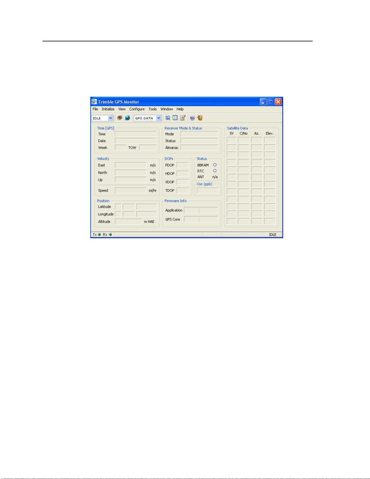
Trimble GPS Monitor Toolkit. . . . . . . . . . . . . . . . . . . . . . . . . . . . . . . . . 17
Install the FTDI USB/Serial Driver Software . . . . . . . . . . . . . . . . . . . . . 17
Connect the PC via the USB Cable . . . . . . . . . . . . . . . . . . . . . . . . . . 18
Start the TGM Application. . . . . . . . . . . . . . . . . . . . . . . . . . . . . . . 20
Connect to the GPS Receiver . . . . . . . . . . . . . . . . . . . . . . . . . . . . . 21
Configure GPS Ports . . . . . . . . . . . . . . . . . . . . . . . . . . . . . . . . . . 23
Configure Output Formats . . . . . . . . . . . . . . . . . . . . . . . . . . . . . . . 24
Configure GPS . . . . . . . . . . . . . . . . . . . . . . . . . . . . . . . . . . . . . 24
Configure PPS Output . . . . . . . . . . . . . . . . . . . . . . . . . . . . . . . . . 25
Configure NMEA Output . . . . . . . . . . . . . . . . . . . . . . . . . . . . . . . 25
Configure TAIP Output . . . . . . . . . . . . . . . . . . . . . . . . . . . . . . . . 26
Creating a Log . . . . . . . . . . . . . . . . . . . . . . . . . . . . . . . . . . . . . 27
Sending Raw Data to device . . . . . . . . . . . . . . . . . . . . . . . . . . . . . . 28
2 PRODUCT DESCRIPTION . . . . . . . . . . . . . . . . . . . . . . . . . 31
Key Features . . . . . . . . . . . . . . . . . . . . . . . . . . . . . . . . . . . . . . . . . 32
Block Diagram . . . . . . . . . . . . . . . . . . . . . . . . . . . . . . . . . . . . . 33
Specifications . . . . . . . . . . . . . . . . . . . . . . . . . . . . . . . . . . . . . . . . . 34
Performance . . . . . . . . . . . . . . . . . . . . . . . . . . . . . . . . . . . . . . 34
Interface . . . . . . . . . . . . . . . . . . . . . . . . . . . . . . . . . . . . . . . . 34
Electrical . . . . . . . . . . . . . . . . . . . . . . . . . . . . . . . . . . . . . . . . 35
Physical. . . . . . . . . . . . . . . . . . . . . . . . . . . . . . . . . . . . . . . . . 35
Environmental . . . . . . . . . . . . . . . . . . . . . . . . . . . . . . . . . . . . . 35
MTBF . . . . . . . . . . . . . . . . . . . . . . . . . . . . . . . . . . . . . . . . . . . . . 36
Absolute Minimum and Maximum Limits . . . . . . . . . . . . . . . . . . . . . . . . . . 37
Normal Operating Conditions. . . . . . . . . . . . . . . . . . . . . . . . . . . . . . . . . 38
Power Consumption Over Temperature and Voltage . . . . . . . . . . . . . . . . . . . . . 39
Run Mode . . . . . . . . . . . . . . . . . . . . . . . . . . . . . . . . . . . . . . . 39
ESD Protection . . . . . . . . . . . . . . . . . . . . . . . . . . . . . . . . . . . . . . . . 39
Ordering Information . . . . . . . . . . . . . . . . . . . . . . . . . . . . . . . . . . . . . 40
Copernicus GPS Receiver 1
Page 7

Table of Contents
3 INTERFACE CHARACTERISTICS . . . . . . . . . . . . . . . . . . . . . 41
Pin Assignments . . . . . . . . . . . . . . . . . . . . . . . . . . . . . . . . . . . . . . . 42
Pin Description . . . . . . . . . . . . . . . . . . . . . . . . . . . . . . . . . . . . . . . . 43
Detailed Pin Descriptions . . . . . . . . . . . . . . . . . . . . . . . . . . . . . . . 44
Protocols . . . . . . . . . . . . . . . . . . . . . . . . . . . . . . . . . . . . . . . . 46
Serial Port Default Settings . . . . . . . . . . . . . . . . . . . . . . . . . . . . . . . . . . 47
GPS Timing. . . . . . . . . . . . . . . . . . . . . . . . . . . . . . . . . . . . . . . . . . 48
Serial Time Output. . . . . . . . . . . . . . . . . . . . . . . . . . . . . . . . . . . 48
A-GPS. . . . . . . . . . . . . . . . . . . . . . . . . . . . . . . . . . . . . . . . . . . . . 50
Enabling A-GPS with the Trimble GPS Monitor Application (TGM) . . . . . . . . 50
Enabling A-GPS with TSIP . . . . . . . . . . . . . . . . . . . . . . . . . . . . . . 51
Pulse-Per-Second (PPS). . . . . . . . . . . . . . . . . . . . . . . . . . . . . . . . . . . . 52
4 OPERATING MODES . . . . . . . . . . . . . . . . . . . . . . . . . . . . 53
Copernicus Receiver Operating Modes. . . . . . . . . . . . . . . . . . . . . . . . . . . . 54
Run Mode . . . . . . . . . . . . . . . . . . . . . . . . . . . . . . . . . . . . . . . 54
Standby Mode . . . . . . . . . . . . . . . . . . . . . . . . . . . . . . . . . . . . . 54
Monitor Mode . . . . . . . . . . . . . . . . . . . . . . . . . . . . . . . . . . . . . 54
Changing the Run/Standby Modes . . . . . . . . . . . . . . . . . . . . . . . . . . . . . . 55
Copernicus Standby Current . . . . . . . . . . . . . . . . . . . . . . . . . . . . . . 55
Using the XSTANDBY Pin to Switch Modes . . . . . . . . . . . . . . . . . . . . . 56
Using Serial Ports to Switch Modes . . . . . . . . . . . . . . . . . . . . . . . . . . 56
18-Hour RTC Roll Over . . . . . . . . . . . . . . . . . . . . . . . . . . . . . . . . . . . 58
Saving Almanac, Ephemeris and Position to Flash Memory. . . . . . . . . . . . . . . . . 59
Graceful Shutdown. . . . . . . . . . . . . . . . . . . . . . . . . . . . . . . . . . . 59
SBAS . . . . . . . . . . . . . . . . . . . . . . . . . . . . . . . . . . . . . . . . . . . . . 59
WAAS. . . . . . . . . . . . . . . . . . . . . . . . . . . . . . . . . . . . . . . . . . . . . 59
Number of channels . . . . . . . . . . . . . . . . . . . . . . . . . . . . . . . . . . 59
Acquisition . . . . . . . . . . . . . . . . . . . . . . . . . . . . . . . . . . . . . . . 60
Usage. . . . . . . . . . . . . . . . . . . . . . . . . . . . . . . . . . . . . . . . . . 60
Almanac collection. . . . . . . . . . . . . . . . . . . . . . . . . . . . . . . . . . . 60
Ephemeris collection. . . . . . . . . . . . . . . . . . . . . . . . . . . . . . . . . . 60
5 APPLICATION CIRCUITS . . . . . . . . . . . . . . . . . . . . . . . . . . 61
Passive antenna—Minimum Connections . . . . . . . . . . . . . . . . . . . . . . . . . . 62
Active Antenna—Full Connection . . . . . . . . . . . . . . . . . . . . . . . . . . . . . . 64
Active Antenna—No Antenna Status. . . . . . . . . . . . . . . . . . . . . . . . . . . . . 66
6 RF LAYOUT CONSIDERATIONS. . . . . . . . . . . . . . . . . . . . . . 69
General Recommendations . . . . . . . . . . . . . . . . . . . . . . . . . . . . . . . . . . 70
Design considerations for RF Track Topologies . . . . . . . . . . . . . . . . . . . . . . . 72
PCB Considerations . . . . . . . . . . . . . . . . . . . . . . . . . . . . . . . . . . . . . 73
Microstrip Transmission Lines. . . . . . . . . . . . . . . . . . . . . . . . . . . . . 73
Stripline Transmission Lines. . . . . . . . . . . . . . . . . . . . . . . . . . . . . . 75
2 Copernicus GPS Receiver
Page 8

Table of Contents
7 MECHANICAL SPECIFICATIONS . . . . . . . . . . . . . . . . . . . . . 77
Mechanical Outline Drawing . . . . . . . . . . . . . . . . . . . . . . . . . . . . . . . . . 78
Soldering the Copernicus GPS Receiver to a PCB . . . . . . . . . . . . . . . . . . . . . . 79
Solder mask . . . . . . . . . . . . . . . . . . . . . . . . . . . . . . . . . . . . . . 79
Pad Pattern . . . . . . . . . . . . . . . . . . . . . . . . . . . . . . . . . . . . . . . 80
Paste Mask . . . . . . . . . . . . . . . . . . . . . . . . . . . . . . . . . . . . . . . 81
8 PACKAGING . . . . . . . . . . . . . . . . . . . . . . . . . . . . . . . . 83
Introduction . . . . . . . . . . . . . . . . . . . . . . . . . . . . . . . . . . . . . . . . . . 84
Reel . . . . . . . . . . . . . . . . . . . . . . . . . . . . . . . . . . . . . . . . . . . . . . 85
Weight . . . . . . . . . . . . . . . . . . . . . . . . . . . . . . . . . . . . . . . . . 85
Tapes . . . . . . . . . . . . . . . . . . . . . . . . . . . . . . . . . . . . . . . . . . . . . 86
9 SHIPPING and HANDLING . . . . . . . . . . . . . . . . . . . . . . . . . 87
Shipping and Handling Guidelines . . . . . . . . . . . . . . . . . . . . . . . . . . . . . . 88
Handling . . . . . . . . . . . . . . . . . . . . . . . . . . . . . . . . . . . . . . . . 88
Shipment . . . . . . . . . . . . . . . . . . . . . . . . . . . . . . . . . . . . . . . . 88
Storage . . . . . . . . . . . . . . . . . . . . . . . . . . . . . . . . . . . . . . . . . 88
Moisture Indicator . . . . . . . . . . . . . . . . . . . . . . . . . . . . . . . . . . . 88
Floor Life. . . . . . . . . . . . . . . . . . . . . . . . . . . . . . . . . . . . . . . . 88
Moisture Precondition . . . . . . . . . . . . . . . . . . . . . . . . . . . . . . . . . . . . 89
Baking Procedure . . . . . . . . . . . . . . . . . . . . . . . . . . . . . . . . . . . . . . . 90
Soldering Paste . . . . . . . . . . . . . . . . . . . . . . . . . . . . . . . . . . . . . . . . 90
Solder Reflow. . . . . . . . . . . . . . . . . . . . . . . . . . . . . . . . . . . . . . . . . 90
Recommended Soldering Profile . . . . . . . . . . . . . . . . . . . . . . . . . . . . . . . 91
Optical Inspection. . . . . . . . . . . . . . . . . . . . . . . . . . . . . . . . . . . . . . . 91
Cleaning. . . . . . . . . . . . . . . . . . . . . . . . . . . . . . . . . . . . . . . . . . . . 92
Soldering Guidelines . . . . . . . . . . . . . . . . . . . . . . . . . . . . . . . . . . . . . 92
Repeated Reflow Soldering . . . . . . . . . . . . . . . . . . . . . . . . . . . . . . 92
Wave Soldering . . . . . . . . . . . . . . . . . . . . . . . . . . . . . . . . . . . . 92
Hand Soldering. . . . . . . . . . . . . . . . . . . . . . . . . . . . . . . . . . . . . 92
Rework . . . . . . . . . . . . . . . . . . . . . . . . . . . . . . . . . . . . . . . . . . . . 92
Conformal Coating . . . . . . . . . . . . . . . . . . . . . . . . . . . . . . . . . . . . . . 92
Grounding the Metal Shield. . . . . . . . . . . . . . . . . . . . . . . . . . . . . . . . . . 93
10 COPERNICUS REFERENCE BOARD . . . . . . . . . . . . . . . . . . . 95
Introduction . . . . . . . . . . . . . . . . . . . . . . . . . . . . . . . . . . . . . . . . . . 96
Reference Board Block Diagram . . . . . . . . . . . . . . . . . . . . . . . . . . . . . . . 98
Reference Board Schematic (page 1 of 3) . . . . . . . . . . . . . . . . . . . . . . . . . . 99
Reference Board Schematic (page 2 of 3) . . . . . . . . . . . . . . . . . . . . . . . . . . 100
Reference Board Schematic (page 3 of 3) . . . . . . . . . . . . . . . . . . . . . . . . . . 101
Reference Board I/O and Power Connector . . . . . . . . . . . . . . . . . . . . . . . . .102
Reference Board Power Requirement. . . . . . . . . . . . . . . . . . . . . . . . . . . . .102
Reference Board Jumper Table . . . . . . . . . . . . . . . . . . . . . . . . . . . . . . . .103
Reference Board Component Locations Drawing . . . . . . . . . . . . . . . . . . . . . . 104
Copernicus GPS Receiver 3
Page 9

Table of Contents
11 FIRMWARE UPGRADE. . . . . . . . . . . . . . . . . . . . . . . . . . . 105
Software Architecture. . . . . . . . . . . . . . . . . . . . . . . . . . . . . . . . . . . . .106
Boot Monitor . . . . . . . . . . . . . . . . . . . . . . . . . . . . . . . . . . . . . . . . .106
Firmware Binary File Format. . . . . . . . . . . . . . . . . . . . . . . . . . . . . . . . . 107
Firmware Loading Procedure . . . . . . . . . . . . . . . . . . . . . . . . . . . . . . . . .107
Pseudo-code . . . . . . . . . . . . . . . . . . . . . . . . . . . . . . . . . . . . . .107
Pseudo-Code Explanation . . . . . . . . . . . . . . . . . . . . . . . . . . . . . . . 109
Error Recovery . . . . . . . . . . . . . . . . . . . . . . . . . . . . . . . . . . . . . 111
Monitor Interface Protocol . . . . . . . . . . . . . . . . . . . . . . . . . . . . . . . . . . 111
Protocol Format . . . . . . . . . . . . . . . . . . . . . . . . . . . . . . . . . . . . 111
Data Transmission . . . . . . . . . . . . . . . . . . . . . . . . . . . . . . . . . . . 111
Monitor Mode Packet Descriptions . . . . . . . . . . . . . . . . . . . . . . . . . . 112
ENQ, ACK, NAK . . . . . . . . . . . . . . . . . . . . . . . . . . . . . . . . . . . 112
Packet ID – 0x96 (Boot ROM Version Report) . . . . . . . . . . . . . . . . . . . . 112
Packet ID – 0x8F (Erase Firmware Section). . . . . . . . . . . . . . . . . . . . . . 113
FlashLoader Tool Reference Guide. . . . . . . . . . . . . . . . . . . . . . . . . . . . . . 116
Introduction . . . . . . . . . . . . . . . . . . . . . . . . . . . . . . . . . . . . . . 116
File and Folder Structure. . . . . . . . . . . . . . . . . . . . . . . . . . . . . . . . 116
Source Code Reference . . . . . . . . . . . . . . . . . . . . . . . . . . . . . . . . 116
Compiling and Generating the Executable. . . . . . . . . . . . . . . . . . . . . . . 117
A TRIMBLE STANDARD INTERFACE PROTOCOL (TSIP) . . . . . . . . . 119
Interface Scope . . . . . . . . . . . . . . . . . . . . . . . . . . . . . . . . . . . . . . . . 120
Run Mode Packet Structure. . . . . . . . . . . . . . . . . . . . . . . . . . . . . . . . . . 120
Automatic Output Packets . . . . . . . . . . . . . . . . . . . . . . . . . . . . . . . . . . 121
Automatic Position and Velocity Reports. . . . . . . . . . . . . . . . . . . . . . . . . . . 122
Initialization Packets to Speed Start-up. . . . . . . . . . . . . . . . . . . . . . . . . . . . 123
Packets Output at Power-Up . . . . . . . . . . . . . . . . . . . . . . . . . . . . . . . . . 123
Timing Packets . . . . . . . . . . . . . . . . . . . . . . . . . . . . . . . . . . . . . . . .124
Satellite Data Packets . . . . . . . . . . . . . . . . . . . . . . . . . . . . . . . . . . . . .124
Backwards Compatibility to Lassen iQ. . . . . . . . . . . . . . . . . . . . . . . . . . . . 124
Recommended TSIP Packets . . . . . . . . . . . . . . . . . . . . . . . . . . . . . . . . . 126
Command Packets Sent to the Receiver . . . . . . . . . . . . . . . . . . . . . . . . . . . 127
Report Packets Sent by the Receiver to the User . . . . . . . . . . . . . . . . . . . . . . . 128
Key Setup Parameters or Packet BB . . . . . . . . . . . . . . . . . . . . . . . . . . . . . 129
Dynamics Code . . . . . . . . . . . . . . . . . . . . . . . . . . . . . . . . . . . .129
Elevation Mask. . . . . . . . . . . . . . . . . . . . . . . . . . . . . . . . . . . . .130
Packet Descriptions . . . . . . . . . . . . . . . . . . . . . . . . . . . . . . . . . . . . . . 131
Packet Descriptions Used in Run Mode . . . . . . . . . . . . . . . . . . . . . . . . 131
Command Packet 0x1E - Clear Battery Backup, then Reset. . . . . . . . . . . . . . 133
Command Packet 0x1F - Request Software Versions . . . . . . . . . . . . . . . . .133
Command Packet 0x21 - Request Current Time. . . . . . . . . . . . . . . . . . . .133
Command Packet 0x23 - Initial Position (XYZ ECEF) . . . . . . . . . . . . . . . . 133
Command Packet 0x24 - Request GPS Receiver Position Fix Mode . . . . . . . . . 134
Command Packet 0x25 - Initiate Soft Reset & Self Test . . . . . . . . . . . . . . .134
4 Copernicus GPS Receiver
Page 10

Table of Contents
Command Packet 0x26 - Request Health . . . . . . . . . . . . . . . . . . . . . . . 134
Command Packet 0x27 - Request Signal Levels. . . . . . . . . . . . . . . . . . . .134
Command Packet 0x2B - Initial Position (Latitude, Longitude, Altitude). . . . . . .134
Command Packet 0x2D - Request Oscillator Offset. . . . . . . . . . . . . . . . . .135
Command Packet 0x2E - Set GPS Time. . . . . . . . . . . . . . . . . . . . . . . .135
Command Packet 0x31 - Accurate Initial Position (XYZ ECEF) . . . . . . . . . . .135
Command Packet 0x32 - Accurate Initial Position,
(Latitude, Longitude, Altitude) . . . . . . . . . . . . . . . . . . . . . . . . . . . 136
Command Packet 0x35 - Set Request I/O Options . . . . . . . . . . . . . . . . . .136
Command Packet 0x37 - Request Status and Values of Last Position and Velocity. . 139
Command Packet 0x38 - Request/Load Satellite System Data . . . . . . . . . . . .139
Command Packet 0x3A - Request Last Raw Measurement . . . . . . . . . . . . . . 140
Command Packet 0x3C - Request Current Satellite Tracking Status . . . . . . . . . 140
Report Packet 0x41 - GPS Time . . . . . . . . . . . . . . . . . . . . . . . . . . . .140
Report Packet 0x42 - Single-Precision Position Fix, XYZ ECEF . . . . . . . . . . .141
Report Packet 0x43 - Velocity Fix, XYZ ECEF . . . . . . . . . . . . . . . . . . . .142
Report Packet 0x45 - Software Version Information . . . . . . . . . . . . . . . . . 142
Report Packet 0x46 - Health of Receiver . . . . . . . . . . . . . . . . . . . . . . .143
Report Packet 0x47 - Signal Levels for all Satellites . . . . . . . . . . . . . . . . .144
Report Packet 0x4A - Single Precision LLA Position Fix. . . . . . . . . . . . . . .145
Report Packet 0x4B - Machine/Code ID and Additional Status. . . . . . . . . . . . 146
Report Packet 0x4D - Oscillator Offset . . . . . . . . . . . . . . . . . . . . . . . . 146
Report Packet 0x4E - Response to Set GPS Time . . . . . . . . . . . . . . . . . . .147
Report Packet 0x55 - I/O Options . . . . . . . . . . . . . . . . . . . . . . . . . . .147
Report Packet 0x56 - Velocity Fix, East-North-Up (ENU) . . . . . . . . . . . . . . 148
Report Packet 0x57 - Information About Last Computed Fix. . . . . . . . . . . . . 149
Report Packet 0x58 - Satellite System Data/Acknowledge from Receiver . . . . . . 149
Report Packet 0x5A - Raw Measurement Data . . . . . . . . . . . . . . . . . . . .152
Report Packet 0x5F . . . . . . . . . . . . . . . . . . . . . . . . . . . . . . . . . .153
Report Packet 0x5C - Satellite Tracking Status . . . . . . . . . . . . . . . . . . . .153
Report Packet 0x6D - All-In-View Satellite Selection. . . . . . . . . . . . . . . . . 154
Command Packet 0x7A . . . . . . . . . . . . . . . . . . . . . . . . . . . . . . . .154
Report Packet 0x7B . . . . . . . . . . . . . . . . . . . . . . . . . . . . . . . . . .155
Command Packet 0x7E - TAIP Message Output . . . . . . . . . . . . . . . . . . . 155
Command Packet 0x82 - SBAS Correction Status . . . . . . . . . . . . . . . . . . . . . .157
Report Packet 0x83 - Double-Precision XYZ Position Fix and Bias Information. . . 158
Report Packet 0x84 - Double-Precision LLA Position Fix and Bias Information. . . 158
Packets 0x8E and 0x8F - Superpacket . . . . . . . . . . . . . . . . . . . . . . . . .159
Command Packet 0xBB - Navigation Configuration . . . . . . . . . . . . . . . . .159
Command Packet 0xBC - Protocol Configuration. . . . . . . . . . . . . . . . . . . 159
Command Packet 0xC0 - Graceful Shutdown and Go To Standby Mode . . . . . . . 160
Command Packet 0xC1 - Set Bit Mask for GPIOs in Standby Mode . . . . . . . . . 162
Command Packet 0xC2 - SBAS SV Mask. . . . . . . . . . . . . . . . . . . . . . .164
TSIP Superpackets . . . . . . . . . . . . . . . . . . . . . . . . . . . . . . . . . . . . . . 165
Command Packet 8E-15 - Set/Request Datum. . . . . . . . . . . . . . . . . . . . .165
Command Packet 0x8E-17 - Request Last Position or Auto-Report Position in UTM
Single Precision Format . . . . . . . . . . . . . . . . . . . . . . . . . . . . . .166
Copernicus GPS Receiver 5
Page 11

Table of Contents
Command Packet 8E-18 - Request Last Position or Auto Report Position in UTM
Double Precision Format . . . . . . . . . . . . . . . . . . . . . . . . . . . . . .166
Command Packet 0x8E-20 - Request Last Fix with Extra Information . . . . . . . .167
Command Packet 0x8E-26 - Non-Volatile Memory Storage . . . . . . . . . . . . . 167
Command Packet 0x8E-2A - Request Fix and Channel Tracking Info, Type 1 . . . . 167
Command Packet 0x8E-2B - Request Fix and Channel Tracking Info, Type 2 . . . . 168
Command Packet 8E-4A - Set/Request Lassen iQ GPS Cable Delay
and PPS Polarity . . . . . . . . . . . . . . . . . . . . . . . . . . . . . . . . . .168
Command Packet 0x8E-4F - Set PPS Width. . . . . . . . . . . . . . . . . . . . . . 168
Report Packet 0x8F-15 - Current Datum Values. . . . . . . . . . . . . . . . . . . . 169
Report Packet 8F-17 - UTM Single Precision Output . . . . . . . . . . . . . . . . . 170
Report Packet 8F-18 - UTM Double Precision Output . . . . . . . . . . . . . . . .171
Report Packet 0x8F-20 - Last Fix with Extra Information (binary fixed point) . . . . 172
Report Packet 0x8F-26 - Non-Volatile Memory Status . . . . . . . . . . . . . . . .174
Report Packet 0x8F-2A - Fix and Channel Tracking Info, Type 1 . . . . . . . . . .174
Report Packet 0x8F-2B - Fix and Channel Tracking Info, Type 2. . . . . . . . . . . 176
Report Packet 0x8F-4F - Set PPS Width. . . . . . . . . . . . . . . . . . . . . . . . 178
Datums . . . . . . . . . . . . . . . . . . . . . . . . . . . . . . . . . . . . . . . . . . . .179
B TRIMBLE ASCII INTERFACE PROTOCOL (TAIP). . . . . . . . . . . . .185
Protocol Overview . . . . . . . . . . . . . . . . . . . . . . . . . . . . . . . . . . . . . . 186
Message Format. . . . . . . . . . . . . . . . . . . . . . . . . . . . . . . . . . . . . . . . 187
Start of a New Message . . . . . . . . . . . . . . . . . . . . . . . . . . . . . . . .187
Message Qualifier . . . . . . . . . . . . . . . . . . . . . . . . . . . . . . . . . . . 187
Message Identifier . . . . . . . . . . . . . . . . . . . . . . . . . . . . . . . . . . . 188
Data String . . . . . . . . . . . . . . . . . . . . . . . . . . . . . . . . . . . . . . . 188
Vehicle ID . . . . . . . . . . . . . . . . . . . . . . . . . . . . . . . . . . . . . . .188
Checksum . . . . . . . . . . . . . . . . . . . . . . . . . . . . . . . . . . . . . . .188
Message Delimiter . . . . . . . . . . . . . . . . . . . . . . . . . . . . . . . . . . .188
Sample PV Message . . . . . . . . . . . . . . . . . . . . . . . . . . . . . . . . . . . . .189
Time and Distance Reporting. . . . . . . . . . . . . . . . . . . . . . . . . . . . . . . . .190
Latitude and Longitude Conversion . . . . . . . . . . . . . . . . . . . . . . . . . . . . . 191
Message Data Strings . . . . . . . . . . . . . . . . . . . . . . . . . . . . . . . . . . . . . 192
AL Altitude/Up Velocity . . . . . . . . . . . . . . . . . . . . . . . . . . . . . . . . . . .193
CP Compact Position Solution . . . . . . . . . . . . . . . . . . . . . . . . . . . . . . . .194
ID Identification Number . . . . . . . . . . . . . . . . . . . . . . . . . . . . . . . . . .195
IP Initial Position. . . . . . . . . . . . . . . . . . . . . . . . . . . . . . . . . . . . . . .196
LN Long Navigation Message . . . . . . . . . . . . . . . . . . . . . . . . . . . . . . . .197
PR Protocol. . . . . . . . . . . . . . . . . . . . . . . . . . . . . . . . . . . . . . . . . .198
PT Port Characteristic . . . . . . . . . . . . . . . . . . . . . . . . . . . . . . . . . . . .199
PV Position/Velocity Solution . . . . . . . . . . . . . . . . . . . . . . . . . . . . . . . . 200
RM Reporting Mode . . . . . . . . . . . . . . . . . . . . . . . . . . . . . . . . . . . . .201
RT Reset Mode . . . . . . . . . . . . . . . . . . . . . . . . . . . . . . . . . . . . . . . . 202
ST Status . . . . . . . . . . . . . . . . . . . . . . . . . . . . . . . . . . . . . . . . . . .203
TM Time/Date . . . . . . . . . . . . . . . . . . . . . . . . . . . . . . . . . . . . . . . .205
VR Version Number . . . . . . . . . . . . . . . . . . . . . . . . . . . . . . . . . . . . .206
6 Copernicus GPS Receiver
Page 12

Table of Contents
X1 Extended Status. . . . . . . . . . . . . . . . . . . . . . . . . . . . . . . . . . . . . .207
Communication Scheme for TAIP . . . . . . . . . . . . . . . . . . . . . . . . . . . . . . 208
Query for Single Sentence . . . . . . . . . . . . . . . . . . . . . . . . . . . . . . . 208
Scheduled Reporting Frequency Interval . . . . . . . . . . . . . . . . . . . . . . . 208
The Response to Query or Scheduled Report . . . . . . . . . . . . . . . . . . . . . 208
The Set Qualifier . . . . . . . . . . . . . . . . . . . . . . . . . . . . . . . . . . . . 209
Sample Communication Session. . . . . . . . . . . . . . . . . . . . . . . . . . . . 209
C NMEA 0183 . . . . . . . . . . . . . . . . . . . . . . . . . . . . . . . . . 211
Overview . . . . . . . . . . . . . . . . . . . . . . . . . . . . . . . . . . . . . . . . . . . 212
The NMEA 0183 Communication Interface . . . . . . . . . . . . . . . . . . . . . . . . . 213
NMEA 0183 Message Format . . . . . . . . . . . . . . . . . . . . . . . . . . . . . . . .213
Field Definitions . . . . . . . . . . . . . . . . . . . . . . . . . . . . . . . . . . . . . . . 214
Invalid Command Set . . . . . . . . . . . . . . . . . . . . . . . . . . . . . . . . . 215
Checksum . . . . . . . . . . . . . . . . . . . . . . . . . . . . . . . . . . . . . . . . . . .215
Exception Behavior . . . . . . . . . . . . . . . . . . . . . . . . . . . . . . . . . . . . . .216
Power-up with No Back-up Data on SRAM. . . . . . . . . . . . . . . . . . . . . . 216
Power-up with Back-up Data on SRAM. . . . . . . . . . . . . . . . . . . . . . . .216
Interruption of GPS Signal. . . . . . . . . . . . . . . . . . . . . . . . . . . . . . .216
General NMEA Parser Requirements . . . . . . . . . . . . . . . . . . . . . . . . . 217
NMEA 0183 Message Options . . . . . . . . . . . . . . . . . . . . . . . . . . . . . . . . 218
NMEA 0183 Message Formats . . . . . . . . . . . . . . . . . . . . . . . . . . . . . . . . 220
GGA - GPS Fix Data. . . . . . . . . . . . . . . . . . . . . . . . . . . . . . . . . .220
GLL - Geographic Position - Latitude/Longitude . . . . . . . . . . . . . . . . . . . 221
GSA - GPS DOP and Active Satellites . . . . . . . . . . . . . . . . . . . . . . . .221
GSV - GPS Satellites in View . . . . . . . . . . . . . . . . . . . . . . . . . . . . . 222
RMC - Recommended Minimum Specific GPS/Transit Data . . . . . . . . . . . . . 223
VTG - Track Made Good and Ground Speed . . . . . . . . . . . . . . . . . . . . .223
ZDA - Time & Date . . . . . . . . . . . . . . . . . . . . . . . . . . . . . . . . . . 224
AH - Almanac Health . . . . . . . . . . . . . . . . . . . . . . . . . . . . . . . . . 225
AL - Almanac Page . . . . . . . . . . . . . . . . . . . . . . . . . . . . . . . . . . 226
AS - Almanac Status . . . . . . . . . . . . . . . . . . . . . . . . . . . . . . . . . .227
BA - Antenna Status . . . . . . . . . . . . . . . . . . . . . . . . . . . . . . . . . .227
CR - Configure Receiver. . . . . . . . . . . . . . . . . . . . . . . . . . . . . . . . 228
EM - Enter Monitor Mode . . . . . . . . . . . . . . . . . . . . . . . . . . . . . . . 228
EP - Ephemeris. . . . . . . . . . . . . . . . . . . . . . . . . . . . . . . . . . . . . 229
IO Ionosphere . . . . . . . . . . . . . . . . . . . . . . . . . . . . . . . . . . . . .231
KG - Set Initial Position . . . . . . . . . . . . . . . . . . . . . . . . . . . . . . . . 231
NM - Automatic Message Output . . . . . . . . . . . . . . . . . . . . . . . . . . .232
PS - PPS Configuration . . . . . . . . . . . . . . . . . . . . . . . . . . . . . . . . 233
PT - Serial Port Configuration . . . . . . . . . . . . . . . . . . . . . . . . . . . . . 234
RT - Reset . . . . . . . . . . . . . . . . . . . . . . . . . . . . . . . . . . . . . . . 235
SG - Set Bit Mask for GPIOs in Standby Mode.. . . . . . . . . . . . . . . . . . . .236
SV - Set Bit Mask for SBAS SV. . . . . . . . . . . . . . . . . . . . . . . . . . . . 238
TF - Receiver Status and Position Fix . . . . . . . . . . . . . . . . . . . . . . . . . 239
UT - UTC . . . . . . . . . . . . . . . . . . . . . . . . . . . . . . . . . . . . . . .240
VR - Version . . . . . . . . . . . . . . . . . . . . . . . . . . . . . . . . . . . . . .241
Copernicus GPS Receiver 7
Page 13

Table of Contents
8 Copernicus GPS Receiver
Page 14

CHAPTER
1
STARTER KIT 1
In this chapter:
Receiver Overview
Starter Kit
Antenna
Quick Start Guide
Trimble GPS Monitor
Toolkit
The Copernicus GPS module is a drop-in
receiver solution that provides position,
velocity, and time data in a choice of three
protocols.
This chapter provides a detailed description of
the starter kit components and instructions for
getting started with interface, hardware setup,
and configuration procedures.
Copernicus GPS Receiver 5
Page 15

1 STARTER KIT
Receiver Overview
Trimble's Copernicus™ GPS receiver delivers proven performance and Trimble
quality for a new generation of position-enabled products. The Copernicus GPS
features the Trimble revolutionary T rimCore™ software technology enabling
extremely fast startup times and high performance in foliage canopy, multipath and
urban canyon environments.
Designed for the demands of automated, pick and place, high-volume production
processes, the Copernicus is a complete 12-channel GPS receiver in a 19mm x 19mm
x 2.54mm, thumbnail-sized shielded unit. The small, thin, single-sided module is
packaged in tape and reel for pick and place manufacturing processes; 28 reflowsolderable edge castellations provide interface to your design without costly I/O and
RF connectors. Each module is manufactured and factory tested to Trimble's highest
quality standards.
The ultra-sensitive Copernicus GPS receiver can acquire GPS satellite signals and
generate fast position fixes with high accuracy in extremely challenging
environments and under poor signal conditions. The module consumes less than
94mW typically at full power with continuous tracking. It has been designed to meet
restrictions on the use of hazardous substances under the RoHS European Directive.
The Copernicus GPS receiver provides position, velocity and time data in a choice of
three protocols: TSIP, TAIP, a nd NMEA. Trimble's TSIP protocol offers complete
control over receiver operation and provides detailed satellite information. The TAIP
protocol is an easy-to-use ASCII protocol designed specifically for track and trace
applications. The bi-directional NMEA 0183 v3.0 protocol offers industry-standard
data messages and a command set for easy interface to mapping software.
Compatible with active or passive antenna designs, the Copernicus GPS receiver is
perfect for portable handheld, battery-powered applications. The receiver's small size
and low power requirement make it ideal for use in Bluetooth appliances, sport
accessories, personal navigators, cameras, computer and communication peripherals,
as well as vehicle and asset tracking, navigation, and security applications.
6 Copernicus GPS Receiver
Page 16

Starter Kit
The Copernicus GPS Starter Kit provides everything you need to get started
integrating state-of-the-art GPS capability into your application. The reference board
provides a visual layout of the Copernicus GPS receiver on a PCB including the RF
signal trace, the RF connector, and the I/O connections of the 28 signal pins. In
addition, the starter kit contains a power converter, power adapter, a GPS antenna,
and software to evaluate the ease with which you can add Copernicus GPS to your
application.
Starter Kit Components
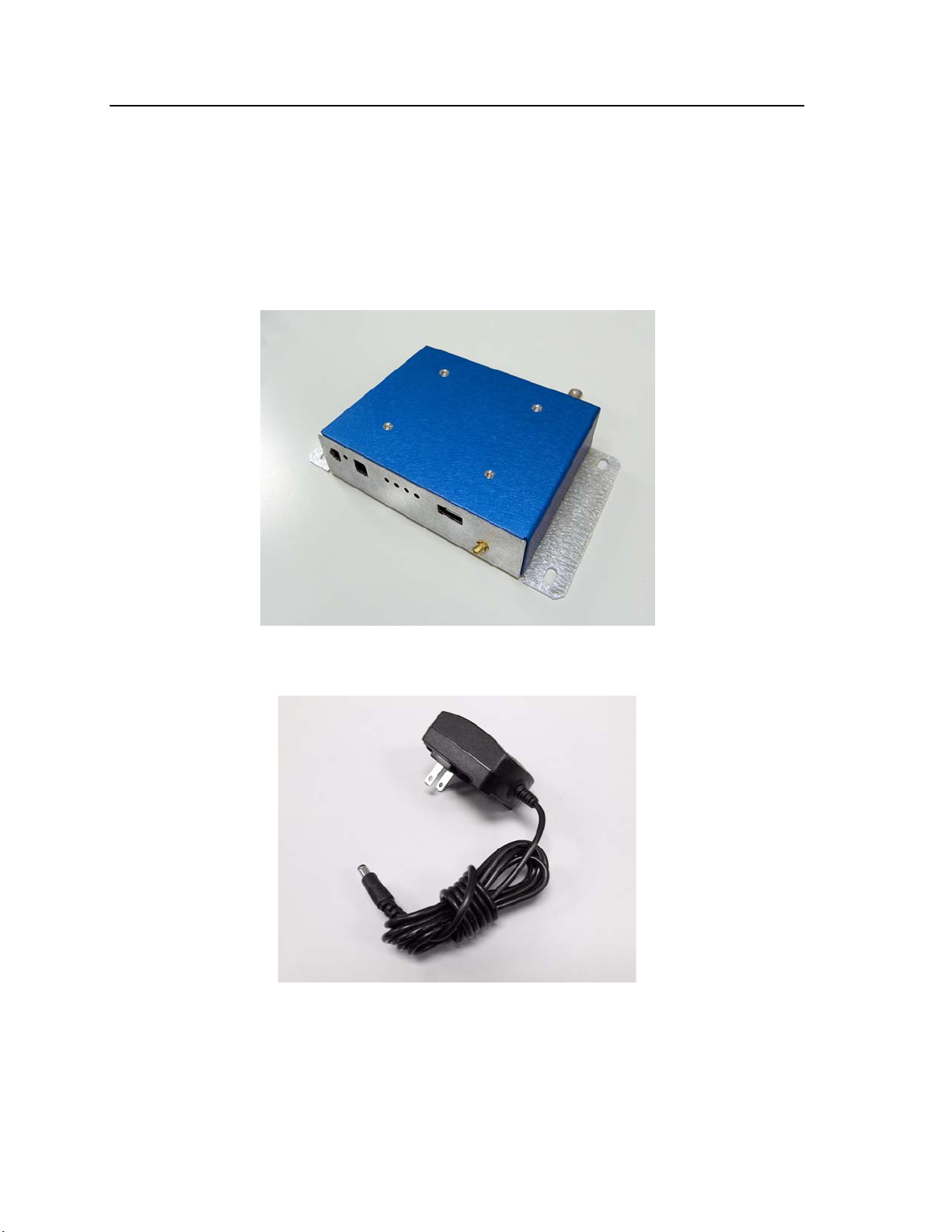
The RoHS compliant (lead-free) Copernicus GPS Starter Kit includes the following:
• Interface unit with reference board and Copernicus GPS receiver
• AC/DC power supply converter
• Universal power adapters for the major standard wall outlets
• Magnetic-mount GPS antenna, 3.3 V, MCX connector, 5 meter cable
• USB cable
STARTER KIT 1
• Cigarette lighter adapter power cable
• Copernicus GPS SMT receivers (3 pieces)
• 14 Jumpers
• Quick Start Guide
• CD containing the SW tools and the Copernicus GPS Reference Manual
Copernicus GPS Receiver 7
Page 17
1 STARTER KIT
Interface Unit
Inside the starter kit interface unit, the Copernicus GPS reference board sits on a shel f
supported by 4 standoffs above the motherboard. The antenna transition cable is
mounted to the outside of the unit and connects to the MCX connector on the
reference board. An 8-wire ribbon cable interfaces the power and I/O between the
reference board and motherboard.
Figure 1.1 Starter Kit Interface Unit
Figure 1.2 AC/DC Power Supply Converter
8 Copernicus GPS Receiver
Page 18
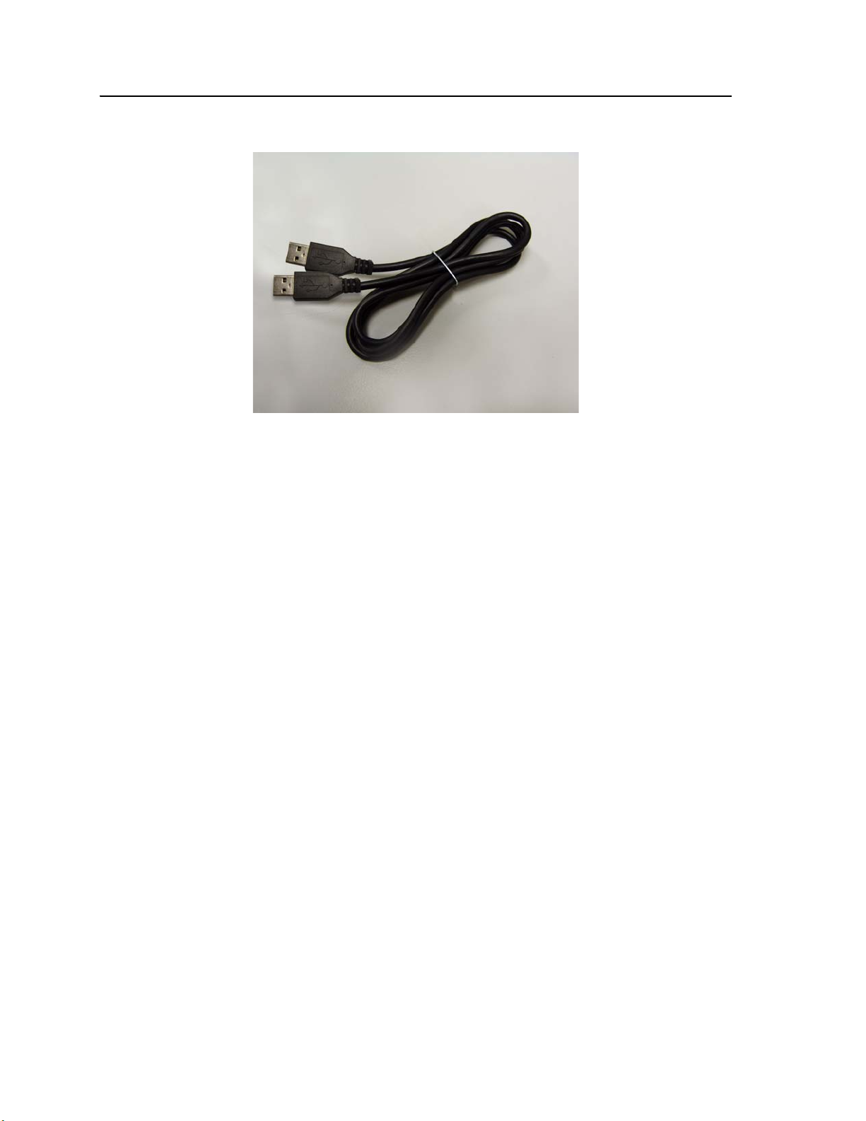
Figure 1.3 USB Cable
STARTER KIT 1
Copernicus GPS Receiver 9
Page 19

1 STARTER KIT
Serial Port Interface
The Copernicus GPS interface unit has a dual port USB interface that is available
through a single A-type USB connection. Before the starter kit can be used with a
USB 2.0-equipped Microsoft Windows (2000, XP)-based PC, the appropriate USB
2.0 drivers must be installed on the PC.
Loading the FTDI Driver
The Copernicus GPS uses a USB 2.0 interface chip from Future T echnology Devices
International Ltd. (FTDI). The FTDI driver must be downloaded and installed on
your PC before you can run the Trimble GPS Monitor (TGM) application used to
communicate with the Copernicus GPS.
1. Use the following URL to access the FTDI drivers:
http://www.ftdichip.com/Drivers/VCP.htm
2. Download and install the appropriate VCP (Virtual COM Port) driver for your
operating system (Win'98 / ME /2000 / XP). Select the option with FT2232C
series support. Follow the instructions provided on the Web site and with the
driver. (http://www.ftdichip.com/Documents/InstallGuides.htm)
3. Use the supplied USB cable to connect the Copernicus GPS interface unit to
your PC. The FTDI driver automatically assigns two (2) virtual COM ports to
the USB port. Use the Windows Device Manager to determine which COM
Ports have been assigned to the USB port.
Default Settings
The default settings on the interface unit USB Port are provided in Table 1.1.
Table 1.1 Serial Port Default Settings
Virtual
Ports
ATXD-A
BTXD-B
Port
Direction
RXD-A
RXD-B
Protocol Baud Rate Data Bits Parity Stop Bits Flow
Control
TSIP-Out
TSIP-IN
NMEA-Out
NMEA-IN
38.4 K
38.4 K
4800
4800
8
8
8
8
None
None
None
None
1
1
1
1
NO
NO
NO
NO
10 Copernicus GPS Receiver
Page 20
STARTER KIT 1
Interface Connections
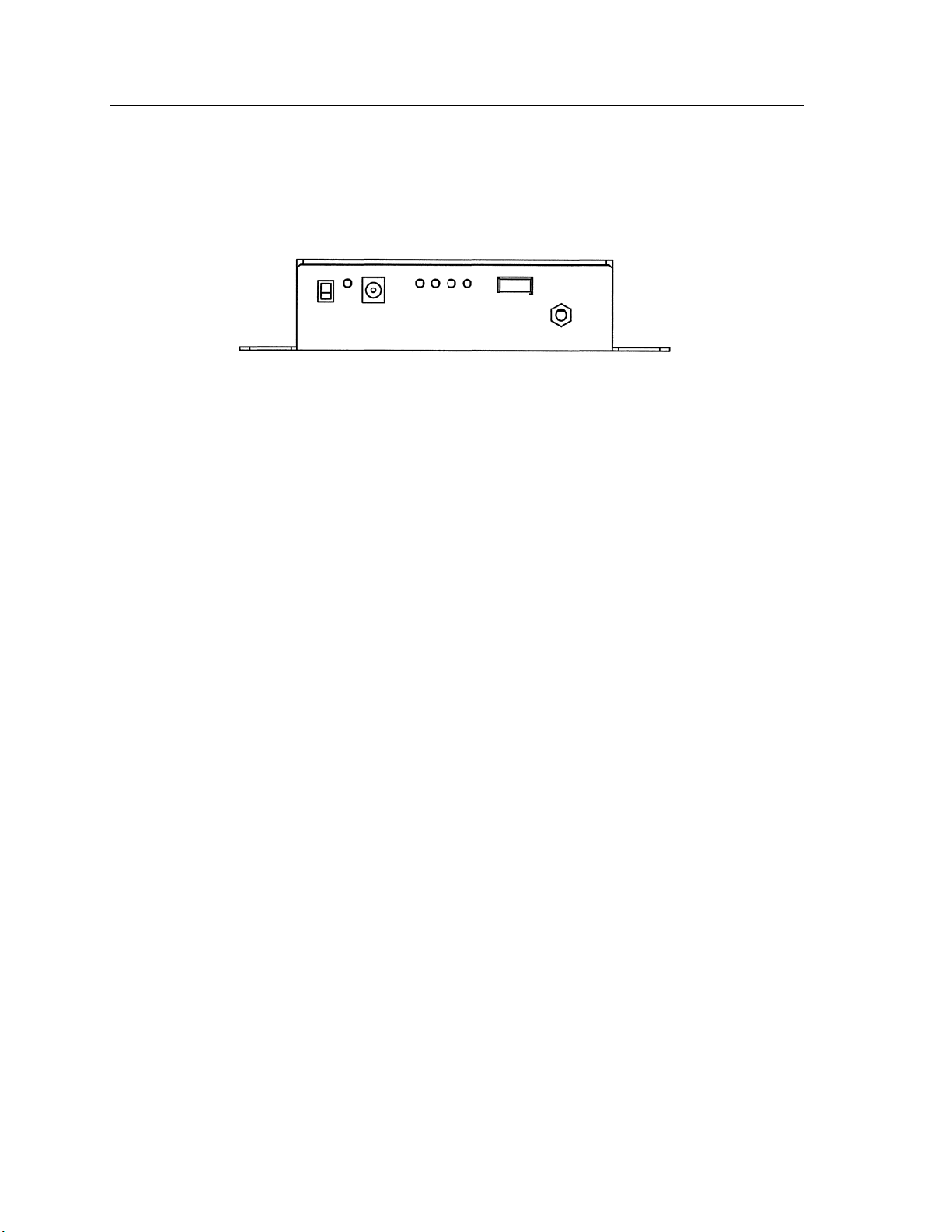
Following is a description of the Copernicus GPS interface unit (numbered references
correlate to numbers in the image below).
8
9
Figure 1.4 Front side of the Interface Unit
6 5 4 3
1. Antenna Connector
The antenna connector is an MCX type connector that is intended to be used
with the supplied 3.0V antenna. This interfaces to the Copernicus GPS
reference board antenna connector.
2. USB Connector
The USB connector is an A-type USB connector that is USB 2.0 and 1.1
compatible. This connection can also be used to power the starter kit and GPS
receiver.
When using the USB connection for power, the PC should be running on AC
power (not battery power) to ensure proper voltage levels to the interface unit.
3. Port A-TX LED
When blinking red, user is transmitting data to the Copernicus GPS receiver on
port A.
4. Port A-RX LED
2
When blinking red, the Copernicus GPS receiver is transmitting data to the
user device on port A.
5. Port B-TX LED
When blinking red, user is transmitting data to the Copernicus GPS receiver on
port B.
6. Port B-RX LED
When blinking red, the Copernicus GPS receiver is transmitting data to the
user device on port B.
Copernicus GPS Receiver 11
Page 21

1 STARTER KIT
7. Power Connector
The power connector (barrel connector) is located on the front right side of the
starter kit. The power connector connects to the AC/DC power converter
supplied with the starter kit. The power converter converts 100 -240 VAC To
12 or 24VDC. The power connector can accept 9 to 32 VDC.
8. Power LED
The Power LED indicates when main power, VCC, is available to the receiver.
Main power is controlled by the Power Switch (#8). When the switch is in the
ON position the LED illuminates Green and VCC is supplied to the receiver.
When the switch is in the OFF position the LED is not lit and the receiver is
powered only by the standby regulator or battery.
Note – For the Copernicus GPS receiver to operate with standby power, the power
source must be from the main power connector (#6) (not from the USB connector).
9. Power Switch
The power switch is used to enable or disable VCC to the receiver.
10. PPS BNC (located on the backside of the interface unit)
The BNC connector provides a 5V TTL level PPS pulse output by the receiver .
The output configuration is controlled by the receiver, not the starter kit driver
circuit. This output is able to drive a 50ohm load.
Note – The Copernicus GPS receiver reference board contains a number of
configuration jumpers for use with various Trimble GPS receivers. Jumpers JP5 and
JP15 must be in place for use with Copernicus GPS receiver.
12 Copernicus GPS Receiver
Page 22

Removing the Reference Board from the Interface Unit
Follow this procedure to remove the Copernicus GPS reference board from the
interface unit:.
1. Before disassembling the interface unit, disconnect the unit from any external
power source and confirm that both you and your work surface are properly
grounded for ESD protection.
2. Remove the four screws, which secure the bottom plate of the interface unit to
the base of the metal enclosure. Set the bottom plate aside.
3. Remove the two screws securing the Copernicus GPS reference board to the
standoffs. These screws are located at opposite ends of the receiver module.
STARTER KIT 1
Copernicus GPS Receiver 13
Page 23
1 STARTER KIT
Antenna
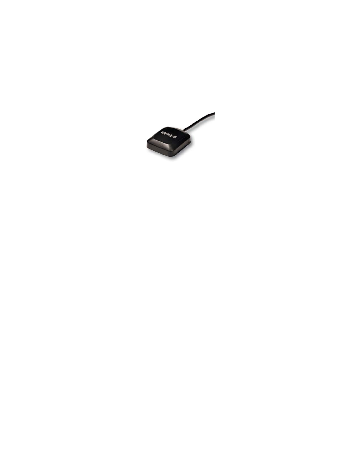
Using a Passive Antenna
The Copernicus GPS Starter Kit comes with an active mini magnetic mount 3.0 V
GPS antenna. This antenna mates with the MCX connector on the interface unit. The
reference board supplies power to the active antenna through the RF transition cable.
To test performance with a passive antenna (not supplied in the Copernicus GPS
Starter Kit) the passive antenna should be connected directly to the MCX connector
on the reference board, to ensure minimal signal loss. Since the passive antenna has
no LNA, the antenna detection and short circuit will not report a true antenna
condition. If the passive antenna is a (DC open) patch antenna, the FW reports an
antenna open condition. If the antenna power jumper is removed, the antenna is
reported as shorted.
14 Copernicus GPS Receiver
Page 24
Quick Start Guide
1. Confirm that you have the following:
– The Copernicus GPS Starter Kit.
– Windows desktop or laptop computer with a USB port.
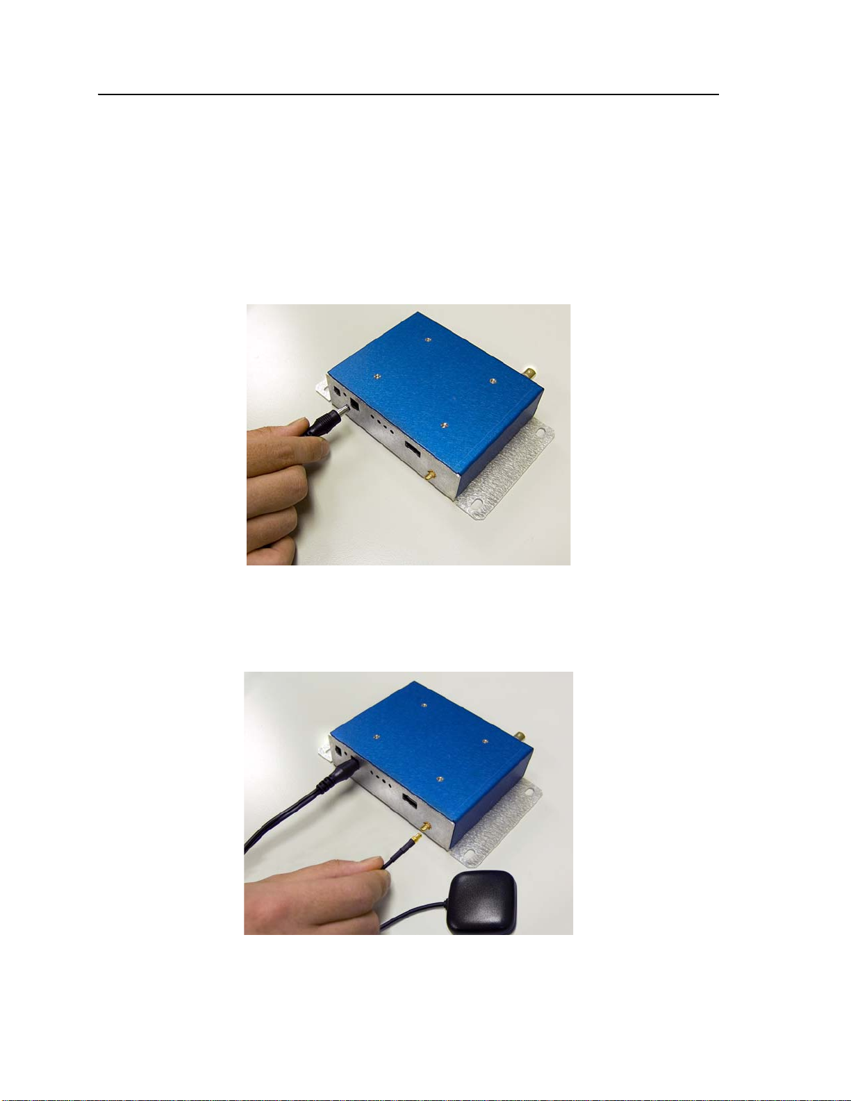
2. Connect the computer’s power cable to the power converter.
3. Plug the power cable into the interface unit.
STARTER KIT 1
Figure 1.5 Connecting Power
4. Plug the power cable into a wall outlet.
5. Connect the magnetic mount GPS antenna to the interface unit.
Figure 1.6 Antenna Connection
6. Place the antenna on the window sill or put the antenna outside.
Copernicus GPS Receiver 15
Page 25
1 STARTER KIT
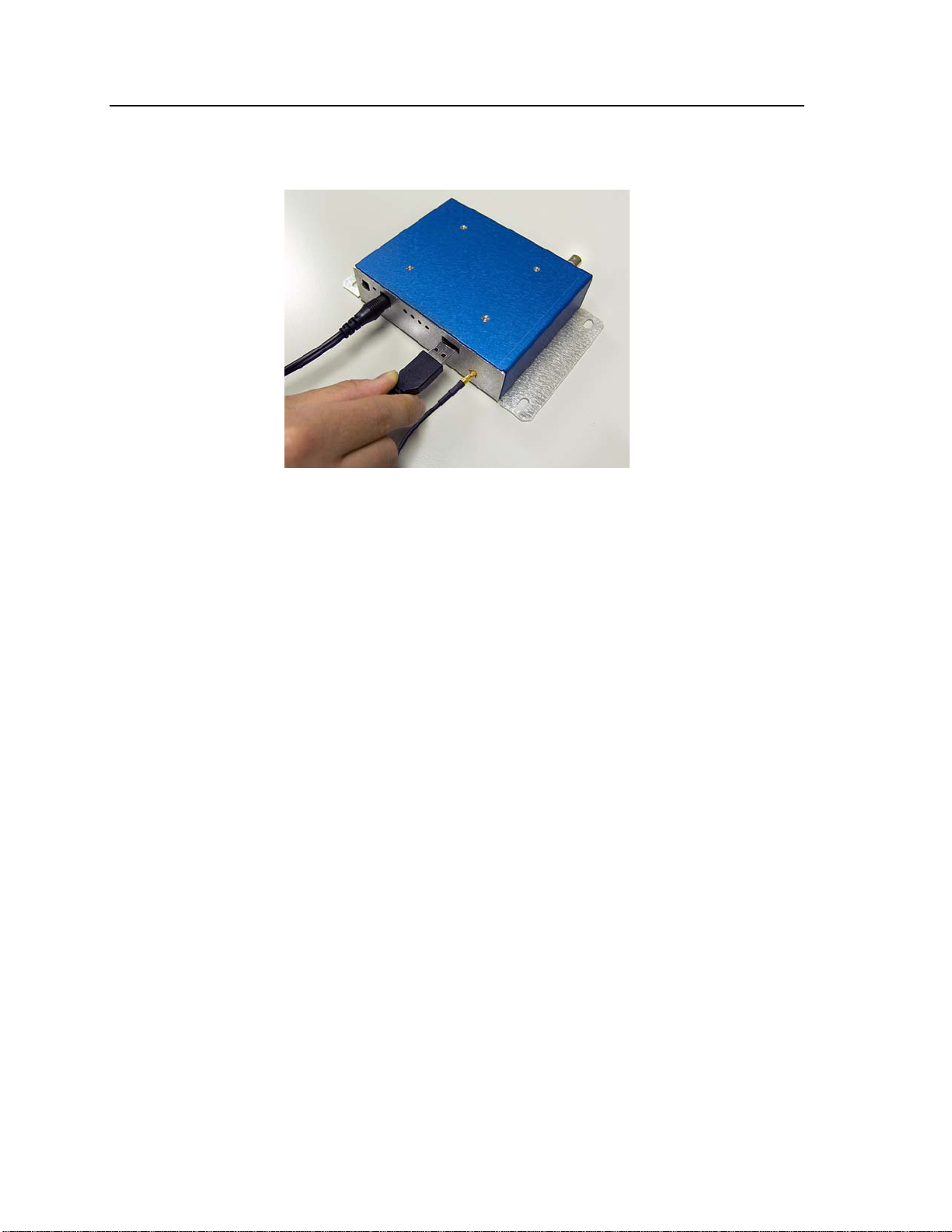
7. Connect the USB cable to the USB connector on the interface unit.
Figure 1.7 Connecting the PC
8. Power-on your computer.
9. Insert the CD found in the starter kit box into your computer CD drive.
10. Install the Trimble GPS Monitor Program from the supplied CD. (see Trimble
GPS Monitor Toolkit, page 17).
11. Download and install the appropriate FTDI driver on your PC (see Install the
FTDI USB/Serial Driver Software, page 17).
12. Execute the Trimble GPS Monitor Program.
13. Select one of the USB virtual COM ports. Either the TSIP or NMEA data
stream is visible on your monitor. To view the other protocol, select a different
USB virtual COM port.
16 Copernicus GPS Receiver
Page 26

Trimble GPS Monitor Toolkit
The Trimble GPS Monitor Tookit is designed to assist you in configuring your
Trimble GPS receiver. The application works with a standard RS-232 serial interface
or the USB interface supplied in the Copernicus GPS starter kit.
TGM includes helpful features such as “Detect Receiver” to test a GPS receiver port
for protocol and baud rate in the event that these settings are lost, the ability to log the
output of multiple GPS devices simultaneously, and the ability send and view
received raw data.
Prior to using the TGM application with a USB interface, you must first download
and install the FTDI USB serial driver software (see instructions below).
Note – The Trimble GPS Monitor application (TGM) replaces many of the previous
“monitor” and “chat” programs used for Trimble Embedded and Resolution T
products.
Install the FTDI USB/Serial Driver Software
The Copernicus GPS starter kit uses a USB 2.0 dual serial port emulator interface
chip from Future Technology Devices International Ltd. (FTDI). Prior to using the
TGM application with a USB interface, you must first download and install the FTDI
USB serial driver software on your PC.
STARTER KIT 1
1. Confirm that you have the following:
– A PC with Windows Vista, Windows XP Service Pack 2, or Windows
2000 Service Pack 4 installed and a free USB port.
– Internet access to complete the installation
2. Download the software for your Trimble product from the Trimble Support
web site http://www.trimble.com/support.shtml, and select the relevant product
link and then the Software Tools option.
3. Select and Save all files to a directory on the hard drive.
4. Install the FTDI driver on your PC.
5. Locate the file called “CDM_Setup.exe” you just saved, and double click it. If
properly installed you should see a FTDI CDM Driver Installation popup
window with the message “FTDI CDM Drivers have been successfully
installed”. Click the OK button.
Copernicus GPS Receiver 17
Page 27
1 STARTER KIT
Connect the PC via the USB Cable
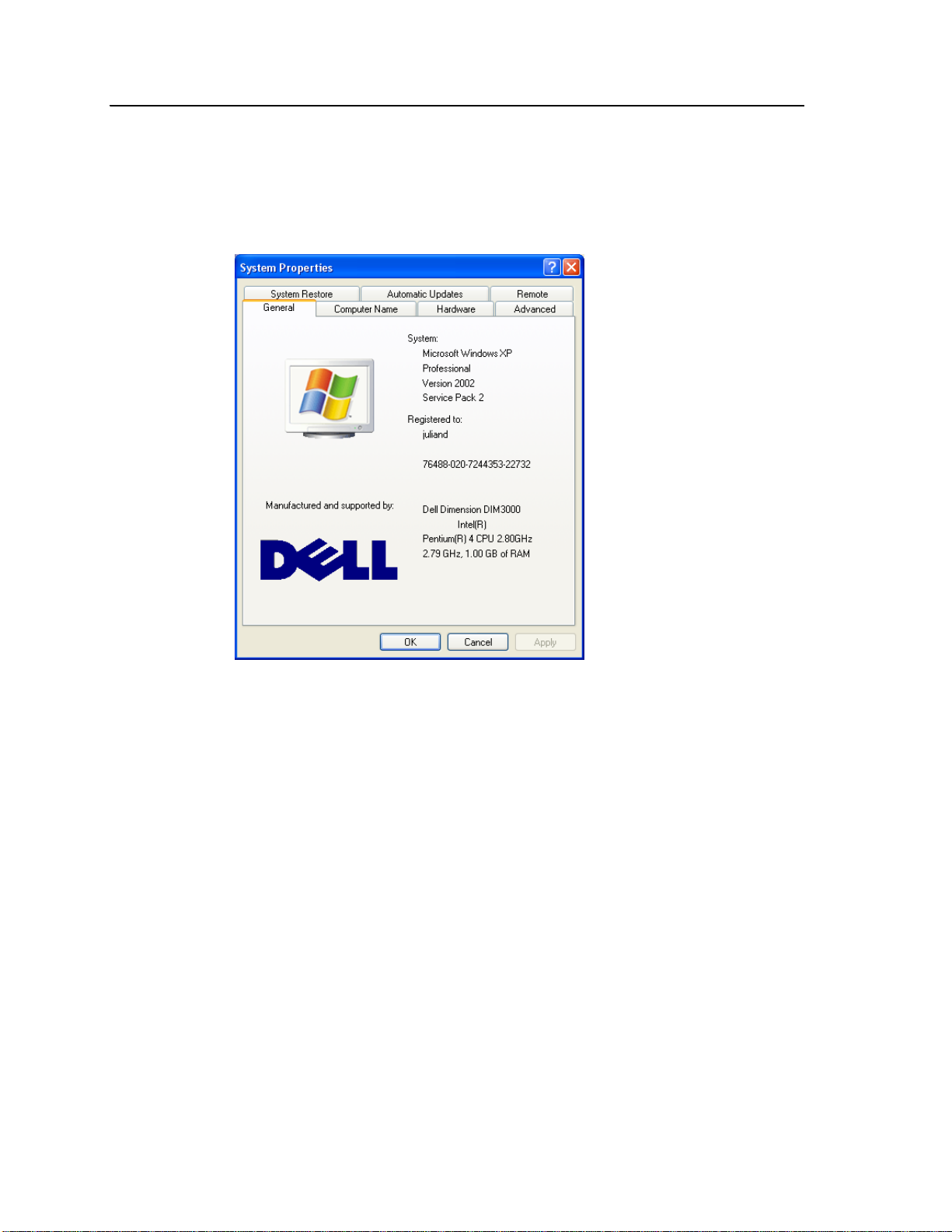
1. Right-click the MyComputer icon.
2. Select the Properties option to view the System Properties Window.
3. Select the Hardware tab.
18 Copernicus GPS Receiver
Page 28
STARTER KIT 1
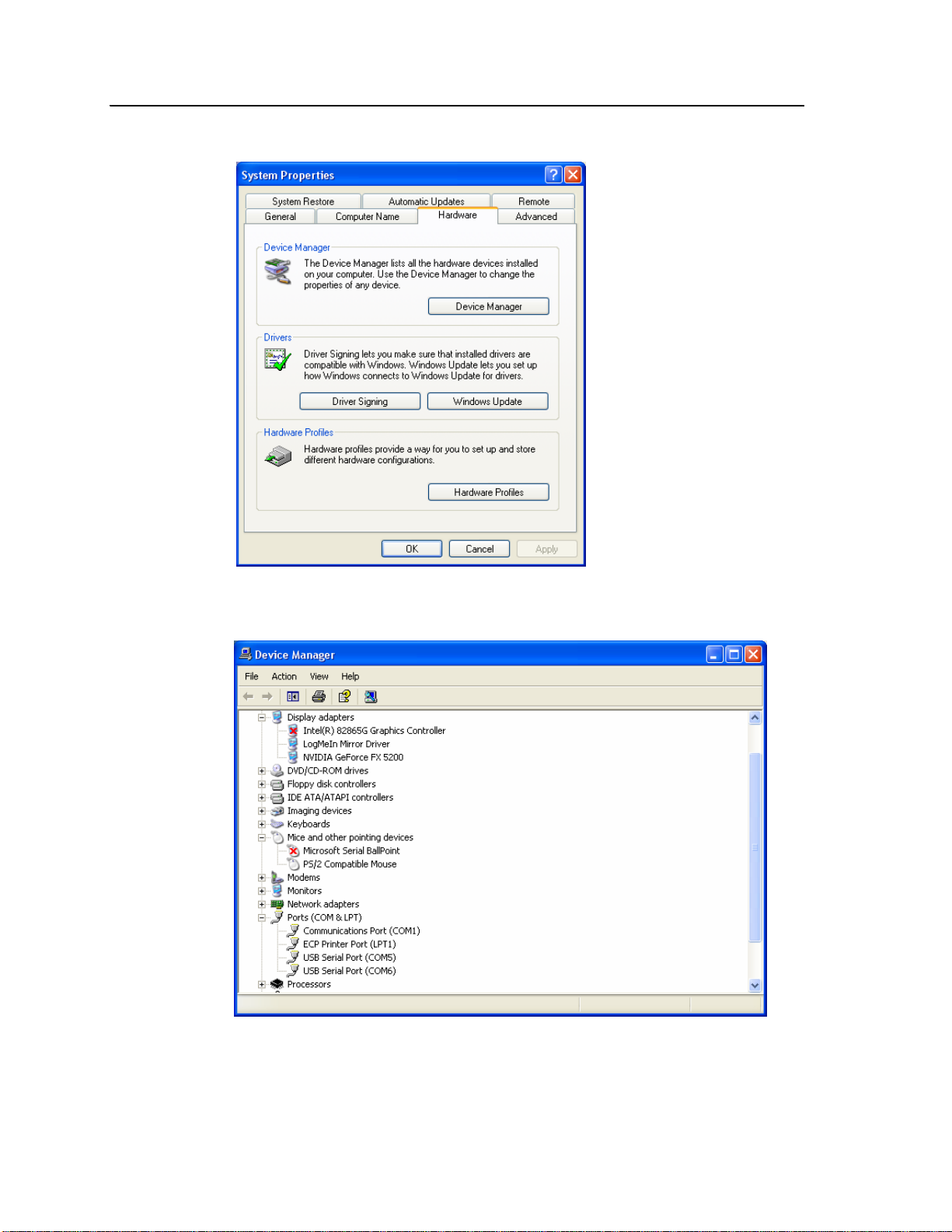
4. Click the Device Manager button.
5. Open the Ports (Com & LPT) section and note down the two USB Serial Port
COM numbers. In the example above they are COM5 and COM6. In general
Port A of the GPS device will be on the lower COM number and Port B will be
on the higher.
Copernicus GPS Receiver 19
Page 29
1 STARTER KIT
Start the TGM Application
1. Go to the directory in which the Trimbl e GPS Monitor application is stored and
open the application. The main window displays.
20 Copernicus GPS Receiver
Page 30
Connect to the GPS Receiver
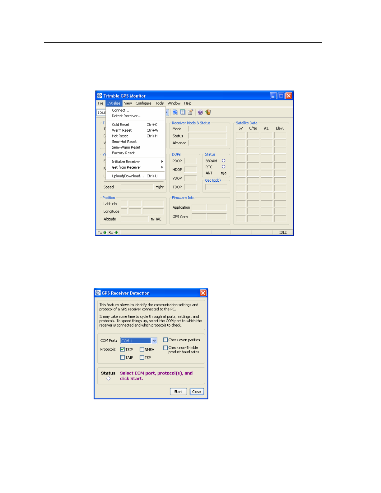
1. Select Initialize > Detect Receiver
STARTER KIT 1
2. Select the port and protocol being used on the module.
If you do not know which protocol is being used you can select TSIP, TA IP and
NMEA. TGM will try each in turn at different baud rates.
Copernicus GPS Receiver 21
Page 31

1 STARTER KIT
3. Click on Yes to accept the discovered connection parameters.
22 Copernicus GPS Receiver
Page 32

Configure GPS Ports
1. Select the Configure pull down menu from the main screen, and select
Receiver Configuration.
STARTER KIT 1
2. Select the Port Configuration tab.
3. Select the required receiver port, baud rate, parity, data bits and stop bits.
4. Select one input and one output protocol.
5. Click the Set button.
6. If the configuration is to be permanent, click Save Configuration.
Copernicus GPS Receiver 23
Page 33

1 STARTER KIT
Configure Output Formats
1. Select the Configure pull down menu from the main screen.
2. Select Receiver Configuration.
3. Select the Outputs tab.
4. After selecting the required setup options, click on Set.
5. If the configuration is to be permanent, click Save Configuration.
Configure GPS
1. Select the Configure pull down menu from the main screen.
2. Select Receiver Configuration.
3. Select the GPS Configuration tab.
4. After selecting the required setup options, click on Set.
5. If the configuration is to be permanent, click Save Configuration.
24 Copernicus GPS Receiver
Page 34

Configure PPS Output
1. Select the Configure pull down menu from the main screen.
2. Select Receiver Configuration.
3. Select the PPS Configuration tab.
STARTER KIT 1
Note – Always ON – the PPS is present even without a GPS fix, it will free run until
fix is obtained. Fixed-based – the PPS will only be output when the r eceiver has a fix.
4. After selecting the required setup options, click on Set.
5. If the configuration is to be permanent, click Save Configuration.
Configure NMEA Output
1. Select the Configure pull down menu from the main screen.
2. Select Receiver Configuration.
3. Select the NMEA tab.
4. After selecting the required setup options, click on Set.
5. If the configuration is to be permanent, click Save Configuration.
Copernicus GPS Receiver 25
Page 35

1 STARTER KIT
Configure TAIP Output
1. Select the Configure pull down menu from the main screen.
2. Select Receiver Configuration.
3. Select the TAIP tab.
4. After selecting the required setup options, click on Set.
5. If the configuration is to be permanent, click Save Configuration.
Note – This screen can only be edited if TAIP is enabled as a port output.
26 Copernicus GPS Receiver
Page 36

Creating a Log
Follow these steps to log the output of the GPS receiver.
1. Select Configure > Data Logging
STARTER KIT 1
2. From the available ports select the com port that connects to your device.
Copernicus GPS Receiver 27
Page 37

1 STARTER KIT
Sending Raw Data to device
3. Create a filename and path in the file field. Use standard file naming if
appropriate with the Unit ID and Test Case number
4. Select the correct protocol and logging options.
5. Click Start Logging.
1. From the Tools Menu select the Generic Packets option.
2. Select the required protocol to send the raw data.
28 Copernicus GPS Receiver
Page 38

STARTER KIT 1
3. Select one of the provided messages from the Presets pull down, or enter your
own data in the Packet Data field.
Note – If entering your own message in the Packet Data, the TGM only requires the
user data not the surrounding start and end bytes. In the example above TSIP user
data is being entered, but TGM already adds the starting DLE and ending DLE/ETX.
4. Click View Raw Data.
5. To view the sent and received data, select the Show Sent Data box.
Copernicus GPS Receiver 29
Page 39

1 STARTER KIT
30 Copernicus GPS Receiver
Page 40

CHAPTER
2
PRODUCT DESCRIPTION 2
In this chapter:
Key Features
Specifications
Interface
MTBF
Absolute Minimum and
Maximum Limits
Normal Operating
Conditions
Power Consumption Over
Temperature and Voltage
ESD Protection
Ordering Information
This chapter describes the Copernicus GPS
Receiver features and performance
specifications.
Copernicus GPS Receiver 31
Page 41

2 PRODUCT DESCRIPTION
Key Features
The Copernicus module is a complete 12-channel GPS receiver in a 19mm x 19mm x
2.54mm, thumbnail-sized shielded unit. The small, thin, single-sided module is
packaged in tape and reel for pick and place manufacturing processes; 28 reflowsolderable edge castellations provide interface to your design without costly I/O and
RF connectors. Each module is manufactured and factory tested to Trimble's highest
quality standards.
• Thumbnail-sized, 19 mm W x 19 mm L (0.75" W x 0.75" L)
• Ultra-thin design, 2.54 mm H (0.1")
• Fast manufacturing: Pick & place assembly, Tape & reel packaging, Reflow
• No I/O or RF connector; 28 Edge castellations
• Ultra-low power usage, less than 94 mW (typical)
• Highly sensitive:
solderable
−150 dBm Tracking Sensitivity
−142 dBm Acquisition Sensitivity
• Fast TTFF (cold start): 39.7 sec
• Supports active or passive antenna designs
• 12-channel simultaneous operation
• Supports SBAS
• Supports NMEA 0183, TSIP and TAIP protocols
• Reference board and starter kit available
• RoHS compliant (lead-free)
32 Copernicus GPS Receiver
Page 42

Block Diagram
PRODUCT DESCRIPTION 2
Figure 2.1 Copernicus GPS Block Diagram
Copernicus GPS Receiver 33
Page 43

2 PRODUCT DESCRIPTION
Specifications
Performance
Performance Specifications
L1 (1575.42 MHz) frequency, C/A code, 12-channel, continuous
tracking receiver
Update Rate
TSIP 1 Hz
NMEA 1 Hz
TAIP 1 Hz
Accuracy (24 hour static)
Horizontal (without SBAS) <2.5 m 50%, <5 m 90%
Horizontal (with SBAS) <2.0 m 50%, <4 m 90%
Altitude (without SBAS) <5 m 50%, <8 m 90%
Altitude (with SBAS) <3 m 50%, <5 m 90%
Velocity 0.06 m/sec
PPS (static)
Acquisition (Autonomous Operation)
Reacquisition 2 sec
Hot Start 3.1 sec
Warm Start 35.4 sec
Cold Start 39.4 sec
Out of the Box 41 sec
Sensitivity
Tracking -150 dBm
Acquisition -142 dBm
Operational
Speed Limit 515 m/s
±100 ns RMS
Interface
34 Copernicus GPS Receiver
Interface Characteristics
Connectors 28 surface mount edge castellations
Serial Port 2 serial ports (transmit/receive)
PPS 3.0 V CMOS-compatible TTL-level pulse, once
per second
Protocols Supports the Trimble Standard Interface
Protocol (TSIP), the Trimble ASCII Interface
Protocol (TAIP), and the National Marine
Electronics Association (NMEA) 0183 v3.0
Bi-directional NMEA Messages
Page 44

Electrical
Electrical Specifications
Prime Power +2.7 VDC to 3.3 VDC
Power Consumption (typ.) 30.7 mA (82.9 mW) @ 2.7 V
Backup Power +2.7 VDC to +3.3 VDC
Ripple Noise Max 50 mV, peak-to-peak from 1 Hz to 1 MHz
Physical
Physical Specifications
Enclosure Metal shield
Dimensions 19 mm W x 19 mm L x 2.54 mm H (0.75" W x
Weight 1.7 grams (0.06 ounce) including shield
Environmental
PRODUCT DESCRIPTION 2
(typ.) 31.3 mA (93.9 mW) @ 3.0 V
0.75" L x 0.1" H)
Environmental Specifications
Operating Temperature -40° C to +85° C
Storage Temperature -55° C to +105° C
Vibration 0.008 g
Operating Humidity 5% to 95% R.H. non-condensing, at +60° C
2
/Hz 5 Hz to 20 Hz
2
/Hz 20 Hz to 100 Hz
0.05 g
-3 dB/octave 100 Hz to 900 Hz
Copernicus GPS Receiver 35
Page 45

2 PRODUCT DESCRIPTION
MTBF
The Mean Time Between Failures (MTBF) of the GPS receiver module was
calculated based on parts count - serial reliability using Telecordia Analysis and
Industry field data for the PCB and Trimble Navigation's field return data (i.e. similar
product or technology parts). This is generally referred to as the Trimble Navigation
Reliability Database, and it consists of the following components:
• Repair Center Data and Field Assessment Analysis
• Supplier FIT goals collected through Commodities Engineering
• Commercial Databases (i.e. Telecordia and MIL-STD-217)
• Trirnble Navigation's Internal Qualification Test Data
• Assumed Duty Cycle, 8760 hours per year
• MTBF at Rated Duty Cycle, 819050 hours MTBF
36 Copernicus GPS Receiver
Page 46

Absolute Minimum and Maximum Limits
Absolute maximum ratings indicate conditions beyond which permanent damage to
the device may occur. Electrical specifications shall not apply when operating the
device outside its rated operating conditions.
Parameter Min Max Unit
Power Supply
Power Supply Voltage (VCC) on
Pin 12
STANDBY Voltage (VCC) on Pin
12 *
Antenna
Input Power at RF Input +10 dBm
Input Gain at RF Input 0 (passive
-0.3 3.6 V
-0.3 3.6 V
antenna)
PRODUCT DESCRIPTION 2
36 dB
Note – See
current.
Input / Output Pin Threshold Levels
Input Pin Voltage (RXD-A, RXD-B, Open, Short, Reserved Pins, Xreset, Xstandby)
Status Min Max Unit
High 2.0 3.6 V
Low 0 0.8 V
Output Pin Voltage (TXD-A, TXD-B, LNA_XEN)
Status Min Max Unit
High (loh = 1 mA) 0.8 * VCC VCC V
Low (lol = 1 mA) 0 0.22 * VCC V
Copernicus Standby Current, page 55 for information on the standby
Copernicus GPS Receiver 37
Page 47

2 PRODUCT DESCRIPTION
Normal Operating Conditions
Minimum and maximum limits apply over full operating temperature range unless
otherwise noted.
Parameter Conditions Min Typ Max Unit
Primary Supply Voltage * The rise time to VCC MUST
be greater than 140 μsecs
Current Draw
Continuous Tracking,
Power Consumption
Continuous Tracking,
Power Consumption
Absolute Maximum
Current Draw **
Standby Mode
Current Draw Standby
Mode RTC Service
Supply Ripple Noise 1Hz to 1MHz
Max: 85°
Min: -40° C, 2.7V
Typ: 25° C, 3.0 V
Max: 85° C, 3.3 V
Min: -40° C, 2.7V
Typ: 25° C, 3.0 V
Max: 85° C,
Min: -40° C
Typ: 25° C, 3.0 V
C, 3.3 V
2.7 3.3 * V
23.9 34.8 38.3 mA
79 93.9 115 mW
50
165
7.1 8.5 60 uA
30
Please see section
Serial Port Activity
50
mA
mW
mA
mVpp
GPS TCXO
Frequency
Hardware RESET Assert XRESET pin to clear
STANDBY memory
* The rise time to VCC MUST be greater than 140 μsecs. The user can use one source of power on Pin 12 (VCC) for both
main and Standby power.
** If using two sources of power, the Main and Standby power must be connected to VCC via an external diode-pair.
During the Standby Mode, the main power can be removed so the unit can be run on Standby power. Standby power
must be at least 0.3V less than main power. The voltage at Pin 12 must be 2.7V to 3.3V including the diode voltage drop.
(See Chapter 5 for information on application circuits.)
±5kHz
100 us
1
mVpp
38 Copernicus GPS Receiver
Page 48

PRODUCT DESCRIPTION 2
Power Consumption Over Temperature and Voltage
Run Mode
(Tracking with Almanac Complete): < 90 mW average @ 2.7 VDC, -40 to 85° C
Standby Mode: < 30 μW @ 3.0 VDC, typical at 25° C, < 200 μW under all
conditions except during service time for the 18-hour real time clock roll over.
At 2.7 volts Avg Current (mA) Avg power consumption (mW)
-40° C 29.7 80.2
Room Temp 30.7 82.9
85
° C 31.5 85.1
At 3.0 volts Avg Current (mA) Avg power consumption (mW)
-40
° C 30.3 90.9
Room Temp 31.3 93.4
85
° C 34.9 104.7
At 3.3 volts Avg Current (mA) Avg power consumption (mW)
-40° C 31.5 104
Room temp 31.4 104
85 v 31.9 105
ESD Protection
ESD testing was performed using JDEC test standard JESD-A114C.01. All inputs
and outputs are protected to ±500 volts ESD level. The RF IN pin is protected up to
1kV.If a higher level of compliance is required, additional electrostatic and surge
protection must be added.
Copernicus GPS Receiver 39
Page 49

2 PRODUCT DESCRIPTION
Ordering Information
Ordering Information
Copernicus GPS Receiver Module Single module in metal enclosure
Reference Board P/N 58054-10
Starter Kit RoHS (Lead-free version): P/N 58050-20
P/N 58048-10
Copernicus GPS module mounted on a carrier
board with I/O and RF connectors for evaluation
purposes, including the RF circuitry with the
antenna open detection, as well as antenna
short detection and protection.
Includes Copernicus Reference Board mounted
on interface motherboard in a durable metal
enclosure, AC/DC power converter, compact
magnetic-mount GPS antenna, serial interface
cable, cigarette lighter adapter, TSIP, NMEA,
and TAIP protocols.
40 Copernicus GPS Receiver
Page 50

CHAPTER
3
INTERFACE CHARACTERISTICS 3
In this chapter:
Pin Assignments
Pin Description
Serial Port Default Settings
GPS Timing
A-GPS
Pulse-Per-Second (PPS)
This chapter provides a detailed description of
the Copernicus GPS Receiver interface.
Copernicus GPS Receiver 41
Page 51

3 INTERFACE CHARACTERISTICS
Pin Assignments
Reserved
Figure 3.1 Copernicus Pin Assignments
42 Copernicus GPS Receiver
Page 52

INTERFACE CHARACTERISTICS 3
Pin Description
Table 3.1 Pin Description
Pin Name Description Function Note
1 GND Ground G Signal ground. Connect to common ground.
2 GND RF Ground G One of two RF grounds adjacent to RF input.
Connect to RF ground system.
3 RF Input GPS RF input I 50-ohm unbalanced (coaxial) RF input.
4 GND RF Ground G One of two RF grounds adjacent to RF input.
Connect to RF ground system.
5 LNA_XEN LNA Enable O Can be used with active antennas only. Active
low logic level signal to control external LNA.
6 Reserved Reserved I/O Do not connect.
7 OPEN Antenna OPEN I Logic level from external antenna detection
circuit. See “Antenna Detect Truth Table”.
8 SHORT Antenna SHORT I Logic level from external antenna detection
circuit. See “Antenna Detect Truth Table”.
9 Reserved Reserved I Con nect to VCC.
10 Reserved Reserved I Connect to VCC.
11 XRESET Reset I Active low logic level reset. Connect to VCC
with or without a pullup resistor, if not used.
12 VCC Supply voltage P Module power supply 2.7 - 3.3 VDC
13 GND Ground G Signal ground. Connect to common ground.
14 GND Ground G Signal ground. Connect to common ground.
15 GND Ground G Signal ground. Connect to common ground.
16 XST ANDBY Run/Standby I Selects “RUN” or “STANDBY” mode. Connect
to VCC if not used (run only).
17 Reserved Reserved I/O Do not connect.
18 Reserved Reserved I/O Do not connect.
19 PPS Pulse per second O Logic level timing signal at 1 Hz. Do not
connect if not used.
20 RXD_B Serial port B receive I Logic level secondary serial port receive.
21 RXD_A Serial port A receive I Logic level primary serial port receive.
22 Reserved Reserved I/O Do not connect.
23 TXD_A Serial port A transmit O Logic level primary serial port transmit.
24 TXD_B Serial port B transmit O Logic level secondary serial port transmit.
25 Reserved Reserved I/O Do not connect.
26 Reserved Reserved I/O Do not connect.
27 GND Ground G Signal ground. Connect to common ground.
28 GND Ground G Signal ground. Connect to common ground.
G: Ground; I: Input; O: Output; P: Power
Copernicus GPS Receiver 43
Page 53

3 INTERFACE CHARACTERISTICS
Detailed Pin Descriptions
RF Input
The RF input pin is the 50 ohm unbalanced GPS RF input, and can be used with
active or passive antennas.
Passive antennas: The RF input pin may be connected by a low-loss 50 ohm
unbalanced transmission system to the passive GPS antenna if loss is minimal
(< 2 dB). It is recommend that you use an external LNA with a passive antenna.
Active Antennas: The RF input pin can also be connected to the output of an external
low-noise amplifier, which is amplifying GPS signals from the antenna. The gain of
the LNA must be great enough to overcome transmission losses from the LNA output
to this pin. The specification for noise figure for the module is < 3 dB at room
temperature and < 4 dB over the specified temperature range, -40 to +85 C. The
external LNA must be located such that the loss from the GPS antenna connection to
the LNA input is minimized, preferably < 1 dB. The noise figure of the LNA should
be as low as possible, preferably< 2 dB. This specification is provided to enable a
cascaded noise figure design calculation. Active antennas must be powered with a
single bias-Tee circuit.
LNA_XEN
This logic level output can be used to control power to an external LNA or other
circuitry. The logic of this signal is such that when the module is running (not in
standby), this signal is low. During “STANDBY” mode, this signal is high. This pin
may be used to control the gate of a p-channel FET used as a switch.
Open/Short Pins
When using an active antenna, it is recommended that you implement an antenna
detection circuit with short circuit protection. There are two pins provided for
reporting the antenna status: OPEN and SHORT.
The logic level inputs outlined in Table 3.2 may be used with a detection circuit (with
or without protection) to monitor the status of the external LNA of an active antenna
by the module.
The truth table for the logic of these signals is provided in Table 3.2. These input pins
conform to the Input / Output Pin threshold levels specified in.
A typical active antenna draws between 10 to 20mA.The antenna Protect/Detect
circuit will trip as a short circuit at around 100mA. It is best to keep the antenna
current below 75mA. An open circuit will be determined if the antenna current falls
below approximately 2mA.
44 Copernicus GPS Receiver
Page 54

INTERFACE CHARACTERISTICS 3
Table 3.2 Antenna Status Truth Table
Condition of logic signals
ANTENNA REPORTS SHORT OPEN
Antenna Open Reported 1 1
Antenna Normal Reported 1 0
Antenna Shorted Reported 0 0
Undefined 0 1
When using a passive antenna with the SHOR T an d OPEN pins floating, the receiver
will report an open condition. If a normal condition from the receiver is desired when
using a passive antenna, set the logic levels of the SHORT pin High and the OPEN
pin Low.
XRESET
This logic-level, active low input is used to issue hardware or power-on reset to the
module. It may be connected to external logic or to a processor to issue reset. To reset
the module, take this pin low for at least 100 microseconds. This pin must be tied to
VCC with a resistance of less than 10 K Ohms if not used.
The hardware reset deletes all the information saved in SRAM (position time,
almanac, ephemeris and customers' user set configurations if not previously saved in
non-volatile Flash memory) and restarts the Copernicus receiver. See Absolute
Minimum and Maximum Limits, page 37 for pin threshold values.
VCC
This is the primary voltage supply pin for the module. This pin also provides power
during Standby Mode (Backup Mode). To setup separate power supplies for main
power and Standby Mode (Backup Mode) power, an external diode-pair must be
provided.
XSTANDBY
This logic level input is used to control the RUN/STANDBY state of the module. If
this signal is High, the unit will run normally. If this signal is Low, the unit will go to
“STANDBY” mode. See Absolute Minimum and Maximum Limits, page 37 for pin
threshold values.
PPS
Pulse-per-second. This logic level output provides a 1 Hz timing signal to external
devices. The positive going 4.2 usec pulse width is controllable by T SIP packet 0x8E4F. The cable delay and polarity is controllable by TSIP packet 0x8E-4A. The PPS
mode is set by TSIP packet 0x35. This output meets the input/output pin threshold
specifications (see Absolute Minimum and Maximum Limits, page 37.)
Copernicus GPS Receiver 45
Page 55

3 INTERFACE CHARACTERISTICS
RXD_A and RXD_B
These logic level inputs are the primary (A) and secondary (B) serial port receive
lines (data input to the module). This output meets the input/output pin threshold
specifications (see Absolute Minimum and Maximum Limits, page 37.) The baud rate
for the two ports is under software control.
TXD_A and TXD_B
These logic level outputs are the primary (A) and secondary (B) serial port transmit
lines (data moving away from the module). This output meets the input/output pin
threshold specifications (see Absolute Minimum and Maximum Limits, page 37.)
The baud rate for the two ports is under firmware control.
Reserved Pins
There are 8 reserved pins on the Copernicus GPS Receiver. For the recommended pin
connections for these reserved pins, see Table 3.1.
Protocols
Table 3.3 Copernicus GPS Receiver Available protocols
Protocols Specification Direction Serial Port
Support
NMEA NMEA 0183 v3.0; Bi-
directional with extended
NMEA sentences
TSIP (Trimble
Standard Interface
Protocol)
TAIP (Trimble ASCII
Interface Protocol)
Trimble propriety binary
protocol
Trimble propriety ASCII
protocol
Input / Output Both Serial Ports
Input / Output Both Serial Ports
Input / Output Both Serial Ports
46 Copernicus GPS Receiver
Page 56

Serial Port Default Settings
The Copernicus GPS Receiver supports two serial ports. The default settings are
provided in the table below.
Table 3.4 Copernicus GPS Receiver Serial Port Default Settings
INTERFACE CHARACTERISTICS 3
Port Port
Direction
A TX D-A 23 TSIP-Out 38.4 K 8 None 1 NO
RXD-A 21 TSIP-IN 38.4 K 8 None 1 NO
B TXD-B 24 NMEA-Out 4800 8 None 1 NO
RXD-B 20 NMEA-IN 4800 8 None 1 NO
Pin # Protocol Characteristics
Baud Rate Data Bits Parity Stop Bits Flow Control
Note – Data Bits, Parity, Stop Bits and Flow Control are not configurable. Only
Protocol and Baud rates are configurable. Detailed descriptions of these protocols
are defined in the Appendices.
Copernicus GPS Receiver 47
Page 57

3 INTERFACE CHARACTERISTICS
GPS Timing
In many timing applications, such as time/frequency standards, site synchronization
systems, and event measurement systems, GPS receivers are used to discipline local
oscillators.
The GPS constellation consists of 24 orbiting satellites. Each GPS satellite contains a
highly-stable atomic (Cesium) clock, which is continuously monitored and corrected
by the GPS control segment. Consequently , the GPS constellation can be considered a
set of 24 orbiting clocks with worldwide 24-hour coverage.
GPS receivers use the signals from these GPS clocks to correct their internal clock
which is not as stable or accurate as the GPS atomic clocks. GPS receivers like the
Copernicus GPS output a highly accurate timing pulse (PPS) generated by an internal
clock which is constantly corrected using the GPS clocks. This timing pulse is
synchronized to UTC within ±100 ns rms.
In addition to serving as a highly accurate stand-alone time source, GPS receivers are
used to synchronize distant clocks in communication or data networks. This
synchronization is possible since all GPS satellite clocks are corrected to a common
master clock. Therefore, the relative clock error is the same, regardless of which
satellite or satellites are used. For timing applications requiring a common clock, GPS
is the ideal solution.
Position and time errors are related by the speed of light. Therefore, a position error
of 100 meters corresponds to a time error of approximately 333 ns. The hardware and
software implementation affects the GPS receiver's PPS accuracy level. The
receiver's clocking rate determines the PPS steering resolution.
Serial Time Output
Time must be taken from the timing messages in the TSIP, TAIP, or NMEA protocols
because position messages contain a timestamp which is usually 1 to 2 seconds in the
past.
Table 3.5 Serial Time Output
Protocol Timing Message
TSIP Report packets 41 and 8F-21
TAIP TM message
NMEA ZDA message
Note – GPS time differs from UTC (Universal Coordinated Time) by a variable,
integer number of seconds UTC=(GPS time)-(GPS UTC offset).
As of January 2006, the GPS UTC offset was 14 seconds. The offset has historically
increased by 1 second about every 18 months. System designers should plan to read
the offset value as a part of the timing interface to obtain UTC. The GPS week
number is in reference to a base week (Week #0), starting January 6, 1980.
48 Copernicus GPS Receiver
Page 58

INTERFACE CHARACTERISTICS 3
Acquiring the Correct Time
To acquire the correct time:
1. Confirm that the almanac is complete and the receiver is generating 3D fixes.
This will eliminate the UTC offset jump.
2. Confirm that the receiver is configured for the late PPS option (i.e., it is only
outputting a PPS on a 3D fix).
3. Capture the time from TSIP packet 0x41 or TSIP packet 0x8F-20 (if using
TSIP).
4. Once time is acquired, on the next PPS add 1 to the whole second to read the
correct time.
Note – The minimum time resolution is 1 second.
Copernicus GPS Receiver 49
Page 59

3 INTERFACE CHARACTERISTICS
A-GPS
The Copernicus GPS Receiver is equipped with assisted GPS (A-GPS), which
enables the receiver to obtain a position fix within seconds using almanac, ephemeris,
time, and position data. This position data can be uploaded to the device via TSIP
packets or the Trimble GPS Monitor (TGM) application. When A-GPS is enabled, the
Copernicus GPS Receiver can achieve fast start-up times characteristic of a hot start.
Follow the procedures below to download current almanac, ephemeris, time, and
position information, and then upload this data to the starter kit module via TGM or
TSIP (to upload position data within the customer application).
C
Warning – To ensure proper format of the ephemeris file and almanac file, a Trimble receiver must
be used to gather this data. Almanac files from non-Trimble receivers may not be in proper format
and thus may not work, (i.e. almanac files downloaded from the Internet).
Enabling A-GPS with the Trimble GPS Monitor Application (TGM)
1. Attach the Copernicus GPS interface unit to your PC.
2. Place the GPS antenna where there is a clear view of sky.
3. Allow the starter kit to run and calculate fixes.
4. On the main screen, wait for the almanac indicator to turn green confirming
that the receiver has collected a current almanac.
Note – It takes 12,5 minutes of uninterrupted Copernicus operation to collect
almanac from the satellites.
5. Click on the initialized pull-down menu and use the download features on the
bottom of the pull-down to download the almanac, position, time and
ephemeris files on your PC.
6. Now that you have collected these files, you can upload them using the upload
features on the initialize pull-down window in TGM.
Note – The collected ephemeris is only good for approximately 2 hours.
50 Copernicus GPS Receiver
Page 60

INTERFACE CHARACTERISTICS 3
Enabling A-GPS with TSIP
1. Allow the receiver to run long enough to collect a current almanac.
Note – It takes 12,5 minutes of uninterrupted Copernicus operation to collect
almanac from the satellites.
2. Use packet 0 x 26 to request the health of the receiver. The response packets
0x46 and 0x4B indicate when the almanac is complete and current.
3. Use packet 0x38 to request the almanac and the ephemeris. The receiver
responds with packet 0 x 58.
4. Use packet 0 x 21 to request time from the receiver. The receiver responds with
packet 0x 41. This data can be used to set your own off-board clock.
5. Use packets 0x42, 0x4A, 0x83 0r 0x84 to request a position from the receiver.
To upload this information back to the receiver, follow this procedures in the
specified order:
1. Upload the time using TSIP packet 0x2E. Wait for upload confirmation report
packet 0x41.
2. Upload position using TSIP packet 0x31 or 0x32. No confirmation report
packet available.
3. Upload the ephemeris using TSIP packet 0x38. Wait for the upload
confirmation report TSIP packet 0x58.
Note – See Appendix A for details on the TSIP protocol.
Copernicus GPS Receiver 51
Page 61

3 INTERFACE CHARACTERISTICS
Pulse-Per-Second (PPS)
The Copernicus GPS receiver provides a CMOS compatible TTL level Pulse-PerSecond (PPS). The PPS is a positive pulse available on pin 19 of the Copernicus GPS
Receiver. The rising edge of the PPS pulse is synchronized with respect to UTC. The
timing accuracy is ±100 rms when valid position fixes are being reported.
The precise UTC or GPS time is reported in TSIP message 0x41 and NMEA message
EDA. The line reports are sent within 500ms after the corresponding PPS.
The rising edge of the pulse is typically less than 6 nanoseconds. The distributed
impedance of the attached signal line and input circuit can affect the pulse shape and
rise time. The PPS can drive a load up to 1mA without damaging the module. The
falling edge of the pulse should not be used.
The Copernicus' default PPS output mode is Always On, sometimes called or “Early
PPS”. In Always On mode, PPS is output immediately after main power is applied.
The PPS is driven by the Real Time Clock (R TC) until the receiver acquires GPS time
from the satellite and begins outputting fixes. In Always On mode, the PPS continues
even if the receiver loses GPS lock. The drift of the PPS, when the Copernicus GPS
receiver is not tracking satellites, is unspecified and should not be used for
synchronization.
The PPS output modes can be controlled with TSIP packet 0x35 and NMEA “PS”
Packet. The modes are Always On (default), Fix Based, or Always Off. Cable delay
compensation is available through the use of TSIP packet 0x8E-4A and NMEA “PS”
Packet. PPS pulse width is controlled by TSIP packet 0x8E-4F and the NMEA “PS”
Packet.
After a specific mode is selected, it can be stored in non-volatile memory (FLASH)
using TSIP command 0x8E-26.
Note – PPS can be configured as positive or negative polarity; factory default is
positive. The PPS pulse width is also configurable; factory default is 4.2
microseconds.
52 Copernicus GPS Receiver
Page 62

CHAPTER
4
OPERATING MODES 4
In this chapter:
Copernicus Receiver
Operating Modes
Run Mode
Standby Mode
Monitor Mode
Changing the Run/Standby
Modes
18-Hour RTC Roll Over
Saving Almanac, Ephemeris
and Position to Flash
Memory
WAAS
This chapter describes the primary Copernicus
GPS Receiver operating modes and provides
guidelines for receiver operation.
Copernicus GPS Receiver 53
Page 63

4 OPERATING MODES
Copernicus Receiver Operating Modes
Table 4.1 Copernicus GPS Receiver Operating Modes
Operating Modes Description
Run Mode Continuous tracking or
normal mode
Standby Mode Backup power or low
power mode
Monitor Mode Flash upgrading mode
Run Mode
The RUN mode is the continuous tracking or the normal mode.
Standby Mode
The Copernicus GPS Receiver provides a S tandby Mode in which the module's RAM
memory is kept alive and the real-time clock is running while the rest of the receiver
is turned off. RAM memory is used to store the GPS almanac, ephemeris, and last
position.
Using this information, together with the time information provided by the real-time
clock, the receiver normally provides faster startup times. The type of start-up after
Standby Mode depends on the state of the receiver prior to entering Standby Mode
and on the length of time the receiver spent in the Standby Mode.
If the receiver has almanac, ephemeris, and position information before entering
Standby Mode, and the time spent in Standby Mode is less than two hours, the
receiver will typically perform a hot start.
If the receiver has all of the information listed above, but the time spent in Standby
Mode is more than two hours, the receiver will typically perform a warm start.
The GPS almanac, ephemeris and recent position are automatically stored in nonvolatile Flash memory. Even without time, the recei ver can use the information stored
in Flash memory to shorten the start-up time. In all cases, the receiver will use all of
the available information to do the fastest start-up possible.
Note – In the Standby Mode, the power consumption of the unit is very low. See
Copernicus Standby Current, page 55.
Monitor Mode
Monitor Mode is the operating mode for upgrading the firmware stored in the Flash
memory. See Chapter 11 for the firmware upgrade procedure.
54 Copernicus GPS Receiver
Page 64

Changing the Run/Standby Modes
There are two methods you can follow to switch the receiver between the Run Mode
and the Standby Mode. Only one of these methods may be used at a time.
1. Using the XSTANDBY pin or
2. Using the serial ports under user control
Note – If you are using the XSTANDBY pin, do not use the serial ports for controlling
the modes. If you are using the serial port option, the XSTANDBY pin should always
be held high. You cannot use serial ports to switch to RUN mode if the XSTANDBY
pin was used to enter STANDBY mode.
Copernicus Standby Current
When the Copernicus GPS Receiver is sent a command to go into Standby Mode,
there is a period of time between 10 and 200 ms (milli seconds) when the power
supply still has to supply almost full operating current. Only after this period has
elapsed will the current draw go down to the specified standby current which is
typically 8.5 uA (micro Amps).
OPERATING MODES 4
Copernicus GPS Receiver 55
Page 65

4 OPERATING MODES
Using the XSTANDBY Pin to Switch Modes
The first method for putting the receiver into Standby Mode or exiti ng this mode back
to the Run Mode is through the pin XSTANDBY, pin #16. As long as the pin is held
high, the receiver will operate normally in Run Mode.
Entering Standby Mode
When the pin is taken low, the receiver will go to the STANDBY mode.
Exiting Standby Mode
When the pin is taken high again, the receiver will perform a hot or warm restart and
return to normal operation. The receiver will hot start if the ephemeris is still valid.
Note – Excessive noise on the XSTANDBY pin could trigger the receiver to reset.
Using Serial Ports to Switch Modes
The second method for putting the receiver into Standby Mode is with TSIP packet
0xC0 or NMEA packet RT.
There are two possible conditions that would trigger the receiver to exit Standby
Mode and reset to normal operations:
1. Serial port activity
2. Exit after X elapsed seconds
56 Copernicus GPS Receiver
Page 66

OPERATING MODES 4
Serial Port Activity
When the receiver enters Standby Mode through the software protocol commands,
the first condition for exiting Standby Mode is using serial port A activity or serial
port B activity. The condition is identical for both ports A and B.
To ensure the receiver detects and responds to serial port activity, issue a NULL
character on the selected serial port to bring the unit out of Standby Mode. In Standby
Mode, the receiver samples for serial port activity at a rate of 32.768 kHz. A NULL
character will bring the selected RX line low for 9 bits so even at the highest baud rate
of 115200, a NULL character should be detectable at the sample rate.
There are two exceptions where serial activity may not trigger the unit to exit Standby
Mode:
• During the 3 seconds following the command to enter Standby Mode.
The Copernicus GPS receiver may not detect serial port activity during the 3
seconds immediately after receiving a software command to enter Standby
Mode. During that 3 seconds, the unit is processing the shut-down command
and will ignore serial port activity. Therefore the minimum time between
issuing the shut-down command and the use of serial port activity to return the
unit to Run Mode is 3 seconds. Standby time cannot be less than 3 seconds.
• During the 10 msec RTC service time.
During the 10 msec RTC service time, there exists a 91.6 μsec window where
the receiver cannot detect serial port activity. Using a series of three NULL
characters in a row should ensure that the unit responds. (See 18-Hour RTC
Roll Over, page 58 for an explanation of the RTC service time.)
Exit after X elapsed seconds.
The second condition that will trigger the receiver to exit Standby Mode is the elapse
of a pre-defined time. When the receiver is placed into the Standby Mode using
protocol commands, the receiver can be made to exit the Standby Mode after a
defined elapsed time using TSIP comman d Pac ket 0 xC0 or N MEA packe t RT. In this
case, the user specifies the number of seconds the receiver should stay in Standby
Mode. After this time has elapsed, the unit will perform a reset and start operating
normally.
Note – These conditions are provided to the receiver in the serial command packet,
and the user can specify any combination of these conditions as desired. For exiting
the Standby Mode, either of the 2 methods can be applied. The first one that occurs
will bring the receiver to the RUN Mode to start normal operations.
Copernicus GPS Receiver 57
Page 67

4 OPERATING MODES
18-Hour RTC Roll Over
If the Standby Mode lasts longer than 18 hours, a special condition will occur. The
real-time clock has a maximum time count of 18 hours, so that every 18 hours the
receiver must briefly power on the processor and read the elapsed time before the
real-time clock rolls over.
The Diagram below describes the Copernicus GPS Receiver current draw levels after
initiating a Standby command, as well as the service time for the 18-hour real time
clock roll over.
IMAGE TO COME
Figure 4.1 Current Draw Levels in Standby Mode
During the 10 msec RTC service is time, there exists a 91.6 μsec window where the
receiver cannot detect state transitions on the RX pins. If NULL characters are being
used to bring the unit out of Standby as described earlier, using three NULL
characters in a row should ensure that one of the NULL characters happens outside of
the vulnerable window so that the serial port activity is detected.
3 Null
= 70 μsec
Figure 4.2 Issuing three (3) NULL Characters for Exiting Standby Mode
91.6
μsec
58 Copernicus GPS Receiver
Page 68

OPERATING MODES 4
Saving Almanac, Ephemeris and Position to Flash Memory
The Almanac, Ephemeris, and recent Position data contained in RAM is
automatically saved to Flash memory.
Graceful Shutdown
The Graceful Shutdown command is issued using TSIP packet 0xC0 or NMEA
command RT with the store RAM to flash flag enabled. The reset type will depend on
the Graceful Shutdown command parameters. On start-up, the unit will use the
almanac, ephemeris, and position from RAM first. If RAM is not available, the unit
will use the almanac from the Flash Memory.
SBAS
The Satellite Based Augmentation System (SBAS) includes implementation of the
current standard for WAAS and the European Geostationary Navigation Overlay
Service (EGNOS) operated by the European Space Agency and other compatible
systems that will come online in the future.
WAAS
Wide Area Augmentation System (WAAS) is an extremely accurate navigation
system developed for civil aviation by the Federal Aviation Administration (FAA).
The system augments GPS to provide the additional accuracy, integrity, and
availability necessary to enable users to rely on GPS for all phases of flight for all
qualified airports within the WAAS coverage area.
The worst-case accuracy is within 7.6 meters of the true position 95% of the time.
This is achieved via a network of ground stations located throughout North America,
which monitor and measure the GPS signal. Measurements from the reference
stations are routed to two master stations, which generate and send the correction
messages to geostationary satellites. Those satellites broadcast the correction
messages back to Earth, where W AAS-enabled GPS receivers apply the corrections to
their computed GPS position.
Number of channels
The Copernicus GPS Receiver tracks one WAAS satellite at a time. When acquiring
and tracking a WAAS satellite, one tracking channel is set aside for this purpose,
leaving eleven tracking channels which are used for the GPS satellites.
Copernicus GPS Receiver 59
Page 69

4 OPERATING MODES
Acquisition
The Copernicus GPS Receiver will acquire a WAAS satellite after it has a GPS-based
position fix. After a two minute position fix outage, the Copernicus module will stop
tracking and acquiring the WAAS satellite. The WAAS satellite will be re-acquired
after a GPS-based position fix is re-established.
Usage
The Copernicus GPS Receiver will only use the data from a WAAS satellite for
position fix corrections. It shall not use a WAAS satellite for the position solution
computation.
Almanac collection
The Copernicus GPS Receiver collects WAAS almanac data and automatically stores
the WAAS Satellite location, and abbreviated almanac and health data to BBRAM
and NVS storage.
Ephemeris collection
The Copernicus GPS Receiver will NOT collect or store WAAS ephemeris data. The
module stores 1 set of WAAS corrections.
60 Copernicus GPS Receiver
Page 70

CHAPTER
5
APPLICATION CIRCUITS 5
In this chapter:
Passive antenna—Minimum
Connections
Active Antenna—Full
Connection
Active Antenna—No
Antenna Status
This chapter describes the Copernicus GPS
Receiver passive and active antenna
connections.
Copernicus GPS Receiver 61
Page 71

5 APPLICATION CIRCUITS
Passive antenna—Minimum Connections
IMAGE TO COME
Figure 5.1 Passive Antenna - Minimum Connections
The minimum connection set for the Copernicus GPS Receiver is illustrated in
Figure 5.1. Following is a description of the schematic.
• A passive antenna is used. The Copernicus GPS Receiver has an on-board
LNA and an Automatic Gain Control circuit.
• The Pin LNA_XEN is not necessary and not connected.
• No Antenna open and short detection or protection is provided.
• If the Open (Pin 7) and Short (Pin 8) are kept unconnected (floating), the
Copernicus GPS Receiver reports an open antenna condition. If a normal
condition report is desired, tie Open low and Short high. (See Table 3.2).
• There is no HW reset ability through the pin XRESET, since XRESET pin is
tied High to VCC.
• There is no HW initiated Standby Mode through the Pin XSTANDBY, since
XSTANDBY pin is tied High to VCC. The software serial command to
Standby Mode will still apply.
• There is no separate power for STANDBY power.
• One serial port is utilized.
62 Copernicus GPS Receiver
Page 72

Figure 5.2 Passive antenna - HW Activated Standby Mode Available
Following is a description of the schematic:
• Passive Antenna is used. The Copernicus GPS Receiver has an on-board LNA
and an Automatic Gain Control circuit.
APPLICATION CIRCUITS 5
• The Pin LNA_XEN is not necessary and not connected.
• There is no HW reset ability through the pin XRESET, since XRESET pin is
tied High to VCC.
• HW initiated Standby Mode through the Pin XSTANDBY is possible, since
XSTANDBY pin is not tied High to VCC. The software serial command to
Standby Mode can still be used as a second method to force the module into
Standby Mode.
• There is no separate power for STANDBY power.
• One serial port is utilized.
• No Antenna open and short detection or protection is provided. When Open
(Pin 7) and Short (Pin 8) are kept unconnected (floating), the Copernicus GPS
Receiver reports an open antenna condition. If a normal condition is desired, tie
Open Low and Short High. See Table 3.2.
Copernicus GPS Receiver 63
Page 73

5 APPLICATION CIRCUITS
Active Antenna—Full Connection
Figure 5.3 Active antenna - Full connection
Following is a description of the schematic with antenna detection, when using a
second source to power the unit when in Standby Mode.
• An active antenna is used.
• The Pin LNA_XEN is connected.
• HW reset ability through the pin XRESET is possible, since XRESET pin is
not tied High to VCC.
• HW initiated Standby Mode through the Pin XSTANDBY is possible, since
XSTANDBY pin is not tied High to VCC. Serial Command to Standby Mode
can still apply as the second method to force the module to Standby Mode.
• A second power source for the standby voltage is applied (see the note below).
• Both serial ports are utilized.
64 Copernicus GPS Receiver
Page 74

APPLICATION CIRCUITS 5
• Antenna open and short detection and protection is provided. The combination
of the two pins Open (Pin 7) and Short (Pin 8) report the antenna status (see
Table 3.2).
Note – When using two power sources, main an d standby , an external di ode pair must
be used to OR the Vcc and Vbackup power to ensure that the voltage at the module
VCC pin is always 2.7-3.3 VDC.
Table 5.2 Component Information
Component Description Manufacturer Part Number
C1 18 PF, 0402 capacitor,
C0G
C2 0.1 uF, 0402 capacitor,
X7R
J1 MCX Connector Johnson Components 133-3711-312
L1 100 nH, 0603 inductor,
surface mount
Q2 PNP Transistor Central Semiconductor CMPT404A
Q3 NPN Transistor Philips MMBT3904
Q4 PNP Transistor Philips MMBT3906
Q5 PNP Transistor Philips MMBT3906
U1 Dual schottky diode Diodes Inc. BAT 54 CT
DI Switching Diode ON Semiconductor MMBD914LTIG
KEMET C0402C180J5GAC
CAL-CHIP GMC04X7R104K16NTLF
Coil Craft 0603CS - R10XJLU
(MMBTA70LT1 may be
used if 12 Volt back
voltage tolerance is not
required)
Copernicus GPS Receiver 65
Page 75

5 APPLICATION CIRCUITS
Active Antenna—No Antenna Status
Figure 5.4 Active antenna - No Antenna Status
66 Copernicus GPS Receiver
Page 76

APPLICATION CIRCUITS 5
Following is a description of this schematic without antenna detection or a separate
power source for Standby Mode:
• An active Antenna is used.
• The Pin LNA_XEN is not connected.
• There is no HW reset ability through the pin XRESET, since XRESET pin is
tied High to VCC.
• HW initiated Standby Mode through the Pin XSTANDBY is possible, since
XSTANDBY pin is not tied High to VCC. Serial Command to Standby Mode
can still apply as the second method to force the module to Standby Mode.
• There is no separate power for STANDBY power.
• Both serial ports are utilized.
• Antenna open and short detection or protection is not provided. If pins 7 and 8
are left floating, they will cause the unit to report an antenna open condition
(see Table 3.2).
Copernicus GPS Receiver 67
Page 77

5 APPLICATION CIRCUITS
68 Copernicus GPS Receiver
Page 78

CHAPTER
6
RF LAYOUT CONSIDERATIONS 6
In this chapter:
General Recommendations
Design considerations for
RF Track Topologies
PCB Considerations
This chapter outlines RF design considerations
for the Copernicus GPS Receiver.
Copernicus GPS Receiver 69
Page 79

6 RF LAYOUT CONSIDERATIONS
General Recommendations
The design of the RF transmission line that connects the GPS antenna to the
Copernicus GPS Receiver is critical to system performance. If the overall RF system
is not implemented correctly, the Copernicus GPS Receiver performance may be
degraded.
The radio frequency (RF) input on the Copernicus GPS module is a 50 ohm,
unbalanced input. There are ground castellations, pins 2 and 4, on both sides of the
RF input castellation, on pin 3. This RF input may be connected to the output of an
LNA which has a GPS antenna at its input or to a passive antenna via a low-loss 50
ohm, unbalanced transmission line system.
In the case where the GPS antenna must be located any significant distance from the
Copernicus GPS Receiver, the use of an LNA at the antenna location is necessary to
overcome the transmission losses from the antenna to the Copernicus GPS module. It
is recommended that in the case of a passive antenna, the transmission line losses
from the antenna to the module be less than 2 dB. Otherwise an LNA should be added
to the system.
The specifications for the external LNA required can be determined as follows. The
specification of noise figure for the Copernicus GPS module is 3 dB at room
temperature and 4 dB over the temperature range −40 C to ±85 C. The noise figure for
this external LNA should be as low as possible, with a recommended maximum of
1.5 dB. It is recommended that the gain of this LNA exceed the loss as measured from
the LNA output to the module input by 10 dB. For example, if the loss from the
external LNA output is 10 dB, the recommended minimum gain for the LNA is 20
dB. In order to keep losses at the LNA input to a minimum, it is recommended that
the antenna be connected directly to the LNA input, with as minimum loss as
possible.
Connections to either the LNA output or to a passive antenna must be made using a
50 ohm unbalanced transmission system. This transmission system may take any
form, such as microstrip, coaxial, stripline or any 50 ohm characteristic impedance
unbalanced, low-loss system.
It is important to keep any noise sources with frequencies at or near 1575 MHz away
from the RF input. In the case of a passive antenna, it is important that the antenna is
not placed in a noisy location (such as too close to digital circuitry) or performance
may be degraded. Shielded transmission line systems (stripline, coaxial) may be used
to route this signal if noise ingress is a concern.
If an active antenna is used and it is desired to power this antenna from the RF
transmission line, a bias-tee will be required at the Copernicus GPS module end. A
simple series inductor (that is parallel resonant at 1575 MHz) and shunt capacitor
(series resonant at 1575 MHz) to which the bias voltage is supplied is sufficient. An
open/short detection and over current protection circuit may also be employed. Please
see Chapter 5, APPLICATION CIRCUITS.
70 Copernicus GPS Receiver
Page 80

RF LAYOUT CONSIDERATIONS 6
In the printed circuit board (PCB) layout, it is recommended to ke ep the copper layer
on which the Copernicus GPS Receiver is mounted clear of solder mask and copper
(vias or traces) under the module. This is to insure mating of the castellations between
the Copernicus GPS module and the board to which it is mounted, and that there is no
interference with features beneath the Copernicus GPS Receiver causing it to lift
during the re-flow solder process.
For a microstrip RF transmission line topology, it is recommended that the layer
immediately below the one to which the Copernicus GPS Receiver is mounted be
ground plane. Pins 2 and 4 should be directly connected to this ground plane with low
inductance connections. Pin 3, the RF input, can be routed on the top layer using the
proper geometry for a 50 ohm system.
Copernicus GPS Receiver 71
Page 81

6 RF LAYOUT CONSIDERATIONS
Design considerations for RF Track Topologies
The following items need to be considered for the Copernicus GPS Receiver RF
layout:
• PCB track connection to the RF antenna input must have impedance of 50
ohms.
• PCB track connection to the RF antenna input must be as short as possible.
• If an external antenna is used, PCB track connection to the RF antenna input
must transition from the circuit board to the external antenna cable, which is
typically a RF connector.
• If there are any ground planes on the same layer as the microstrip trace, please
refer to the Coplaner Waveguide design. Not covered in this manual.
• PCB track connection to the RF antenna input must be routed away from
potential noise sources such as oscillators, transmitters, digital circuits,
switching power supplies and other sources of noise.
• RF and bypass grounding must be direct to the ground plane through its own
low-inductance via
• Active or passive antennas may be used. If using a passive antenna the
connection to the antenna input shall be very short. It is possible to mount the
patch antenna on the same PCB as the Copernicus GPS module. Designers
must be aware of noise generating circuitry and proper design precautions
taken (shielding,.).
The PCB track connection to the RF antenna input must not have:
• Sharp bends.
• Components overlaying the track.
• Routing between components to avoid undesirable coupling.
72 Copernicus GPS Receiver
Page 82

PCB Considerations
The minimum implementation is a two-layer PCB substrate with all the RF signals on
one side and a solid ground plane on the other. Multilayer boards can also be used.
Two possible RF transmission line topologies include microstrip and stripline.
Microstrip Transmission Lines
RF LAYOUT CONSIDERATIONS 6
Figure 6.1 Microstrip Transmission Lines
Ground Plane Design Recommendation
Use a complete ground plane immediately under the PCB layer on which the
Copernicus module is mounted. Around the signal tracks on the same layer as the
module, flood or “copper pour” and connect to the ground p lane using low inductan ce
vias. A single ground plane is adequate for both analog and digital signals.
Design of Microstrip Transmission Line
Connections to either the LNA output or to a passive antenna must be made using a
50 ohm unbalanced transmission system. The PCB parameters that affect impedance
are:
• Track width (W)
• PCB substrate thickness (H)
• PCB substrate permittivity (ε
)
r
Copernicus GPS Receiver 73
Page 83

6 RF LAYOUT CONSIDERATIONS
• To a lesser extent, PCB copper thickness (T) and proximity of same layer
ground plane.
Figure 6.2 PCB Microstrip Topology
Table 6.1 shows typical track widths for an FR4 material PCB substrate (permittivity
of 4.6 at 1.5 GHz) and different PCB thickness. One ounce copper is assumed for
ε
r
the thickness of the top layer. If a Multi layer PCB is used, the thickness is the
distance from signal track to nearest ground plane.
Table 6.1 Typical Track Widths for an FR4 material PCB Substrate in Microstrip
Topology
Substrate Material Permittivity Substrate Thickness
H (mm)
1.6 2.91
1.2 2.12
1.0 1.81
FR4 4.6 0.8 1.44
0.6 1.07
0.4 0.71
0.2 0.34
Track Width
W (MM)
Microstrip Design Recommendations
It is recommended that the antenna connection PCB track be routed around the
outside of the module outline, kept on a single layer and have no bends greater than
45 degrees. It is not recommended, for production reasons, to route the track under
the module.
74 Copernicus GPS Receiver
Page 84

Stripline Transmission Lines
.
Figure 6.3 Stripline Transmission Lines
Ground plane design in stripline topology
• The stripline topology requires three PCB layers: two for ground planes and
one for signal. One of the ground plane layers may be the layer to which the
Copernicus GPS module is mounted. If this is the case,
RF LAYOUT CONSIDERATIONS 6
• The top layer must be flooded with ground plane and connected to all ground
castellations on the Copernicus GPS module.
• The RF input should be connected to the signal layer below using a via.
• The layer below the signal layer is the second ground plane.
• Connect the two ground planes with vias typically adjacent to the signal trace.
• Other signals of the Copernicus GPS module may be routed to additional layer
using vias.
For the symmetric stripline topology where the signal trace is equal distance from
each ground plane, the following table applies:.
Table 6.2 Typical track widths for an FR4 material PCB substrate in Stripline topology
Substrate Material Permittivity Substrate Thickness
H (mm)
1.6 0.631
1.2 0.438
1.0 0.372
FR4 4.6 0.8 0.286
0.6 0.2
0.4 0.111
0.2 N/A
Track Width
W (MM)
Copernicus GPS Receiver 75
Page 85

6 RF LAYOUT CONSIDERATIONS
76 Copernicus GPS Receiver
Page 86

CHAPTER
7
MECHANICAL SPECIFICATIONS 7
In this chapter:
Mechanical Outline
Drawing
Soldering the Copernicus
GPS Receiver to a PCB
This chapter provides product drawings and
instructions for soldering the Copernicus GPS
Receiver to a PCB.
Copernicus GPS Receiver 77
Page 87

7 MECHANICAL SPECIFICATIONS
Mechanical Outline Drawing
IMAGE TO COME
Top View
Figure 7.1 Copernicus GPS Receiver, Footprint
Figure 7.2 Copernicus GPS Receiver, Outline Dimensions
Bottom View
78 Copernicus GPS Receiver
Page 88

MECHANICAL SPECIFICATIONS 7
Soldering the Copernicus GPS Receiver to a PCB
Solder mask
When soldering the Copernicus GPS Receiver to a PCB, keep an open cavity
underneath the Copernicus module (i.e., do not place copper traces or solder mask
underneath the module). The diagram below illustrates the required user solder mask.
The units in brackets, [ ], are in millimeters.
No solder mask
or copper traces
under the unit.
Figure 7.3 Solder Mask Diagram
Copernicus GPS Receiver 79
Page 89

7 MECHANICAL SPECIFICATIONS
Pad Pattern
Below is the required user pad pattern. The units in brackets, [ ], are in millimeters.
No solder mask
or copper traces
under the unit.
Figure 7.4 Pad Pattern Diagram
80 Copernicus GPS Receiver
Page 90

MECHANICAL SPECIFICATIONS 7
Paste Mask
To ensure good mechanical bonding with sufficient solder to form a castellation
solder joint, use a solder mask ratio of 1:1 with the solder pad. When using a 5 ±1 Mil
stencil to deposit the solder paste, we recommend a 4 Mil toe extension on the stencil.
The units in brackets, [ ], are in millimeters.
Figure 7.5 Paste Mask Diagram
Copernicus GPS Receiver 81
Page 91

7 MECHANICAL SPECIFICATIONS
82 Copernicus GPS Receiver
Page 92

CHAPTER
8
PACKAGING 8
In this chapter:
Introduction
Reel
Tapes
Follow the instructions in this chapter to ensure
the integrity of the packaged and shipped
Copernicus GPS Receiver modules.
Copernicus GPS Receiver 83
Page 93

8 PACKAGING
Introduction
The Copernicus GPS modules is packaged in tape and reel for mass production. The
reel is sealed in a moisture proof Dry Pack bag. Please follow all the directions
printed on the package for handling and baking.
The Copernicus GPS modules are packaged in two quantities: reel with 100 pieces
and reel with 500 pieces.
Figure 8.1 Copernicus GPS Receiver Packaged in Tape
84 Copernicus GPS Receiver
Page 94

Reel
PACKAGING 8
The 13-inch reel that can be mounted in a standard feeder for the surface mount pick
and place machine. The reel dimensions are the same regardless of the quantity on the
reel.
Figure 8.2 Reel Diagram
Weight
100 pcs with reel packaging + desiccant + humidity indicator = approximately
0.79Kg (1.74 lbs.)
500 pcs with reel packaging + desiccant + humidity indicator = approximately
1.47Kg (3.24 lbs.)
100 pcs with reel packaging + desiccant + humidity indicator + white pizza box =
approximately 1.02Kg (2.24 lbs.)
500 pcs with reel packaging + desiccant + humidity indicator + white pizza box =
approximately 1.70Kg (3.74 lbs.)
Copernicus GPS Receiver 85
Page 95

8 PACKAGING
Tapes
The tape dimensions illustrated in the diagram below are in inches. The metric units
appear in brackets [ ].
Figure 8.3 Tape Diagram
Made in China
S/N 05011234
52979-00-D
Made in China
Made in China
S/N 05011234
52979-00-D
Figure 8.4 Feeding Direction Diagram
Made in China
S/N 05011234
52979-00-D
Feeding direction
S/N 05011234
52979-00-D
ROUND HOLE
Made in China
Made in China
S/N 05011234
52979-00-D
S/N 05011234
52979-00-D
86 Copernicus GPS Receiver
Page 96

CHAPTER
9
SHIPPING and HANDLING 9
In this chapter:
Shipping and Handling
Guidelines
Moisture Precondition
Baking Procedure
Soldering Paste
Solder Reflow
Recommended Soldering
Profile
Optical Inspection
Cleaning
Soldering Guidelines
Rework
Conformal Coating
Grounding the Metal Shield
This chapter provides detailed guidelines for
shipping and handling the Copernicus GPS
Receiver to ensure compliance with the product
warranty.
Copernicus GPS Receiver 87
Page 97

9 SHIPPING and HANDLING
Shipping and Handling Guidelines
Handling
The Copernicus GPS module is shipped in tape and reel for use with an automated
surface mount machine. This is a lead-free module with silver plating. Do not allow
bodily fluids or lotions to come in contact with the bottom of the module.
C
WARNING – The Copernicus GPS module is packed according to ANSI/EIA-481-B and J-
STD-033A. All of the handling and precaution procedures must be followed. Deviation
from following handling procedures and precautions voids the warranty.
Shipment
The reel of Copernicus GPS modules is packed in a hermetically sealed moisture
barrier bag (DryPac) then placed in an individual carton. Handle with care to avoid
breaking the moisture barrier.
Storage
The shelf life for the sealed DryPac is 12 months and it must be stored at <40 °C and
<90% relative humidity.
Moisture Indicator
A moisture indicator is packed individually in each DryPac to monitor the
environment. All five indicating spots are shown blue from the factory. If the
indicator shows pink, follow the instructions printed on the indicator and bake as
necessary. See Baking Procedure, page 90 for baking instructions.
Floor Life
The reel of Copernicus GPS modules is vacuum sealed in a moisture barrier bag
(DryPac). Once the bag is opened, moisture will bond with the modules. In a
production floor environment, an open reel needs to be processed within 72 hours,
unless it is kept in a nitrogen purged dry chamber. If the moisture indicator has
changed to pink, follow the baking instructions printed on the moisture barrier.
The Copernicus GPS is a lead free component for RoHS compliance. This unit is also
plated with immersion silver for better solderability . The silver may tarnish over time
and show yellow in color, but tarnish should not affect the solderability.
C
88 Copernicus GPS Receiver
WARNING – Operators should not touch the bottom silver solder pads by hand or with
contaminated gloves. No hand lotion or regular chlorinated faucet water can be in
contact with this module before soldering.
Page 98

Moisture Precondition
Precautions must be taken to minimize the effects of the reflow thermal stress on the
module. Plastic molding materials for integrated circuit encapsulation are
hygroscopic and absorb moisture dependent on the time and the environment.
Absorbed moisture will vaporize during the rapid heating of the solder reflow
process, generating pressure to all the interface areas in the package, followed by
swelling, delamination, and even cracking of the plastic. Components that do not
exhibit external cracking can have internal delamination or cracking which affects
yield and reliability.
SHIPPING and HANDLING 9
Figure 9.1 Moisture Precondition Label
Copernicus GPS Receiver 89
Page 99

9 SHIPPING and HANDLING
Baking Procedure
If baking is necessary, Trimble recommends baking in a nitrogen purge oven.
Temperature: 125 °C
Duration: 24 Hours.
After Baking: Store in a nitrogen-purged cabinet or dry box to prevent
absorption of moisture.
C
WARNING – Do not bake the units within the tape and reel packaging.Repeated baking
processes will reduce the solderablity.
Soldering Paste
The Copernicus GPS module itself is not hermetically sealed, Trimble strongly
recommends using the “No Clean” soldering paste and process. The castellation
solder pad on this module is plated with silver plating. Use Type 3 or above soldering
paste to maximize the solder volume. An example is provided below.
Solder paste: Kester EM909
Alloy composition: Sn96.5Ag3Cu.5 (SAC305) 96.5% Tin/ 3%Silver/ 0.5%
Liquidus Temperature:221 °C
Stencil Thickness: 5 Mil (0.005")
Stencil opening requires 4-mil toe over paste in the X and Y directions.
Note – Consult solder paste manufacturer and the assembly process for the approved
procedures.
Copper
Solder Reflow
A hot air convection oven is strongly recommended for solder reflow. For the leadfree solder reflow , we recommend using a nitrogen-purged oven to increase the solder
wetting. Reference IPC-610D for the lead free solder surface appearance.
C
90 Copernicus GPS Receiver
WARNING – Follow the thermal reflow guidelines from the IPC-JEDEC J-STD-020C.
The size of this module is 916.9 mm3. According to J-STD-020C, the peak
component temperature during reflow is 245 +0 °C.
Page 100

Recommended Soldering Profile
SHIPPING and HANDLING 9
Figure 9.2 Recommended Soldering Profile
Select the final soldering thermal profile very carefully. The thermal profile depends
on the choice of the solder paste, thickness and color of the carrier board, heat
transfer, and size of the penalization.
C
WARNING – For a double-sided surface-mount carrier board, the unit must be placed on
the secondary side to prevent falling off during reflow.
Optical Inspection
After soldering the Copernicus GPS module to the carrier board, follow IPC-610
specification to visually inspect using 3X magnification lens to verify the following:
• Each pin is properly aligned with mount pad.
• Pads are properly soldered.
• No solder is bridged to the adjacent pads. X-ray the bottom pad if necessary.
Copernicus GPS Receiver 91
 Loading...