

Page 1

MZ-6SER Manual
PC/104 bus compatible ZFx86
SBC with six serial ports
Manufactured by
TRI-M ENGINEERING
Engineered Solutions for Embedded Applications
Technical Manual
P/N: MZ-6SER-MAN-V2
Revision: 24/04/03
TRI-M ENGINEERING
1407 Kebet Way, Unit 100
Port Coquitlam, BC V3C 6L3
Canada
http://www.Tri-M.com
Tel 604.945.9565
North America 800.665.5600
Fax 604.945.9566
Page 2

24/04/2003 MZ-6SER Manual
©
2001, Tri-m Engineering
No part of this document may be reproduced, transmitted, transcribed, stored in a retrieval
system, or translated into any language or computer language, in any form or by any means,
electronic, mechanical, magnetic, optical, chemical, manual, or otherwise, without the express
written permission of Tri-M Engineering.
Disclaimer
This document is for information use only. Tri-M Engineering makes no representations or
warranties with respect to the content of this manual and specifically disclaims any implied
warranty of merchantability or fitness for any particular purpose. Tri-M Engineering is under no
circumstances liable for incidental or consequential damages or related expenses resulting
from the use of this product, even if it has been notified of the possibility of such damage. TriM Engineering reserves the right to revise this publication from time to time without obligation
to notify any person of such revisions. To ensure that you have the most recent version,
please visit our website at www.tri-m.com.
Warning
A working knowledge of electronics and PC-technology is required to use this
product.
Pay attention to electrostatic discharges. Use a CMOS protected workplace.
Disconnect power source when connecting any cables or devices.
This is a high-technology product.
A working knowledge of electronics and
PC-technology is required!
Page 3

Page 4
24/04/2003 MZ-6SER Manual
Table of contents
CHAPTER 1: GENERAL INFORMATION ............................................................................................................. 4
1.1 GENERAL DESCRIPTION............................................................................................................................... 4
1.2 SPECIFICATIONS ......................................................................................................................................... 5
1.3 EMBEDDED FEATURES ................................................................................................................................6
CHAPTER2: INSTALLATION............................................................................................................................... 7
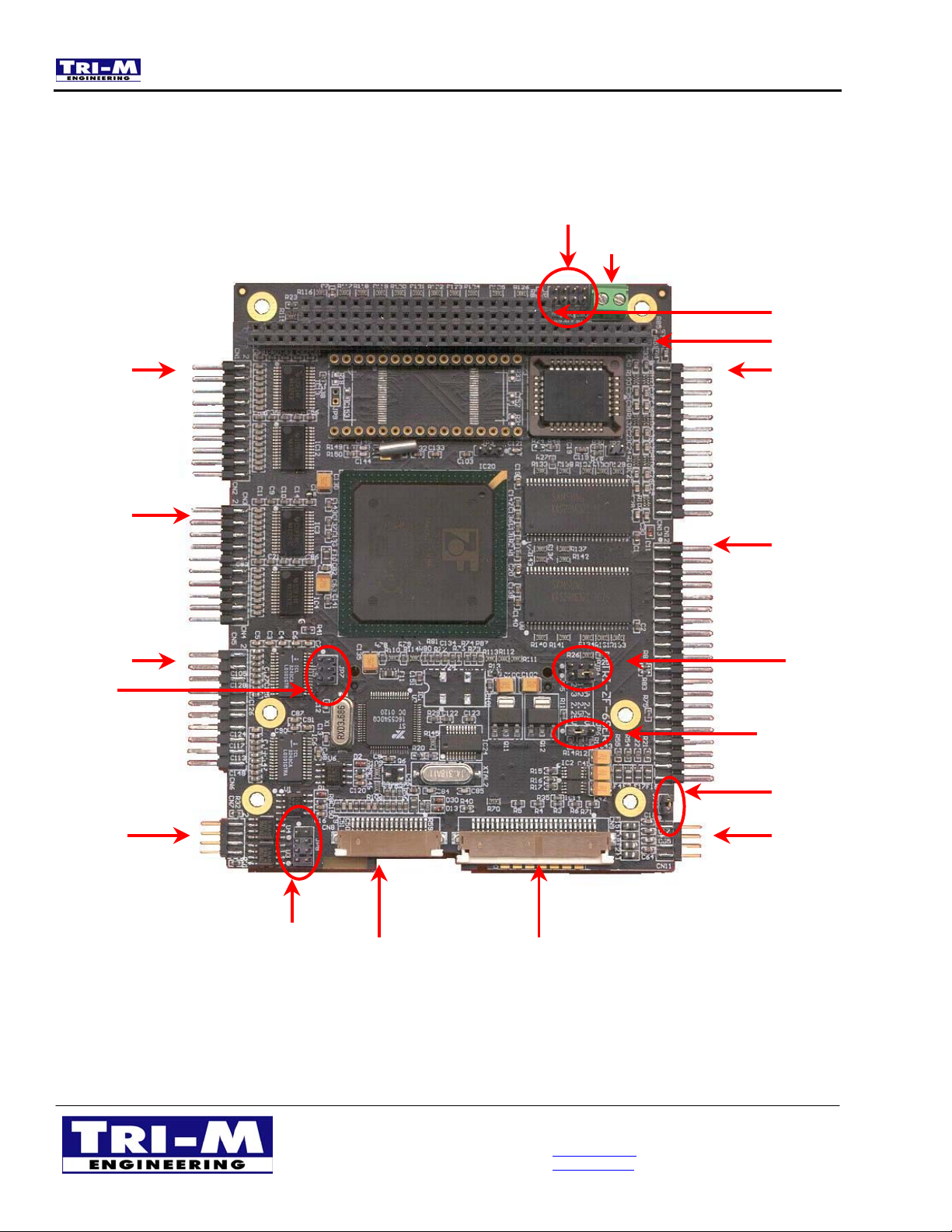
2.1 LOCATING THE CONNECTORS & JUMPERS .................................................................................................... 7
CHAPTER 3: JUMPERS...................................................................................................................................... 10
3.1 CLOCK MULTIPLIER SELECT (JP1).............................................................................................................. 10
3.2 PCI CLOCK DIVIDER (JP1) ........................................................................................................................11
3.3 WRITE ENABLE JUMPER FOR BIOS FLASH (JP2) ......................................................................................... 11
3.4 WATCHDOG TIMER (JP3) ..........................................................................................................................11
3.5 MASTER /SLAVE MODE SELECT (JP4)........................................................................................................ 12
3.6 CPU CLOCK OSCILLATOR SELECT (JP5) ................................................................................................... 12
3.7 CPU CORE VOLTAGE SELECT (JP6).......................................................................................................... 13
3.8 ENABLE RS232 DRIVERS FOR SERIAL 5 AND SERIAL 6 PORT (JP7) ............................................................13
CHAPTER 4: CONNECTORS.............................................................................................................................. 15
4.1 SERIAL INTERFACES (CN1 TO CN6) ..........................................................................................................15
4.2 UTILITY CONNECTOR (CN8) ......................................................................................................................19
4.3 FLOPPY INTERFACE (CN9) ........................................................................................................................ 20
4.4 Z-TAG CONNECTOR (CN10) ......................................................................................................................20
4.5 USB 1,2 CONNECTOR (CN11).................................................................................................................. 20
4.6 IDE INTERFACE (CN12)............................................................................................................................ 20
4.7 PARALLEL (CN13) ....................................................................................................................................22
4.8 PC/104 CONNECTORS (CN14, AND CN15).............................................................................................. 23
4.9 EXTERNAL POWER (CN16)........................................................................................................................ 24
4.10 CMOS & RTC BATTERY HOLDER (CN17)................................................................................................. 25
4.12 INTERRUPT AND I/O PORT ASSIGNMENTS ................................................................................................... 26
CHAPTER 5: BIOS SETTINGS ...........................................................................................................................28
5.1 BIOS SETUP ............................................................................................................................................28
APPENDIX 1: OPTIONAL UTIL104+ UTILITY BOARD .................................................................................. 29
APPENDIX 2: LITERATURE REFERENCES .................................................................................................. 30
Tri-M Engineering Tel: 800.665.5600, 604.945.9565
1407 Kebet Way, Unit 100 Fax: 604.945.9566
Port Coquitlam, BC V3C 6L3 E-mail: [email protected]
Canada Web site: www.tri-m.com
2
Page 5

24/04/2003 MZ-6SER Manual
List of Tables
Table 1: Jumper List...................................................................................................................7
Table 2: Clock Multiplier Select (JP1).......................................................................................10
Table 3: PCI Clock Divider (JP1).............................................................................................. 11
Table 4: Watchdog Jumper (CN16)......................................................................................... 12
Table 5: Master/Slave Mode Select (JP4) ................................................................................12
Table 6: CPU Clock select (JP5).............................................................................................. 12
Table 7: CPU Core Voltage Select (JP6) .................................................................................13
Table 8: Serial 5 and 6 RS232 Driver Disable (JP7) ................................................................13
Table 9: Half/Full Duplex Routing (JP8) ...................................................................................13
Table 10: Bur/Boot Rom Select (JP10) ....................................................................................14
Table 11: MZ-6SER Connector List..........................................................................................15
Table 12: Serial Port Resources ..............................................................................................16
Table 13: RS232 Serial Ports Com1 (CN1) and Com2 (CN2).................................................. 16
Table 14: RS232 Serial Ports Com3 (CN3) and Com4 (CN4).................................................. 16
Table 15: RS232 Serial Ports Com5 (CN5) and Com6 (CN6).................................................. 17
Table 16: RS485 Serial Connector (CN7) for Half Duplex Mode.............................................. 18
Table 17: RS485 Serial Connector (CN7) for Full Duplex Mode .............................................. 18
Table 18: Utility connector (CN8) ............................................................................................. 19
Table 19: Floppy Interface (CN9) ............................................................................................ 20
Table 20: USB 1,2 Connector (CN11) ......................................................................................20
Table 21: Hard Disk Resources ...............................................................................................21
Table 22: IDE Drive Interface (CN12).......................................................................................21
Table 23: Parallel Port Resources............................................................................................22
Table 24: Parallel Port Connections (CN13) ............................................................................22
Table 25: PC/104 8bit Connector (CN14)................................................................................23
Table 26: PC/104 16bit Connector (CN15)..............................................................................24
Table 27: External Power Connector (CN16) ........................................................................... 24
Table 28: Compact Flash Connector (CN18) ...........................................................................25
Table 29: IRQ Interrupt.............................................................................................................26
Table 30: I/O Port..................................................................................................................... 27
Table 31: MZ104+UTIL104 Interface .......................................................................................29
List of Figures
Figure 1: Connector and Jumper location MZ-6SER top............................................................8
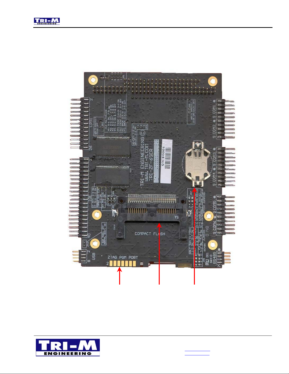
Figure 2: Connector and Jumper location MZ-6SER back .........................................................9
Figure 3: MZ104+UTIL Utility Connector Board .......................................................................29
Tri-M Engineering Tel: 800.665.5600, 604.945.9565
1407 Kebet Way, Unit 100 Fax: 604.945.9566
Port Coquitlam, BC V3C 6L3 E-mail: [email protected]
Canada Web site: www.tri-m.com
3
Page 6

24/04/2003 MZ-6SER Manual
CHAPTER 1: GENERAL INFORMATION
1.1 General Description
The MZ-6SER is an embedded system controller measuring just 3.63 inches x 4.86 inches,
which incorporates the revolutionary ZFx86 “PC-on-a-chip” processor. The MZ-6SER offers
the quickest route of integrating a full x86 AT-compatible computer into your embedded control
application. In addition, the built-in peripherals minimize the number of additional modules
required. By combining the system hardware, I/O, software, and solid-state mass storage, the
MZ-6SER lowers your exposure to possible development risks, costs and significantly reduces
your time-to-market.
The MZ-6SER’s fully compatible PC/104 embedded expansion bus, permits easy integration to
a wide selection of low-cost hardware peripherals. The numerous features provide an ideal
price/performance solution.
Tri-M Engineering Tel: 800.665.5600, 604.945.9565
1407 Kebet Way, Unit 100 Fax: 604.945.9566
Port Coquitlam, BC V3C 6L3 E-mail: [email protected]
Canada Web site: www.tri-m.com
4
Page 7

24/04/2003 MZ-6SER Manual
1.2 Specifications
586 CPU
32-bit CPU core operating at 33Mhz to 128Mhz
8K byte Level 1 cache, write back and write through support
Floating point unit
PC Core Logic with PCI enhancement
32 bit 33MHz PCI rev 2.1 compliant “Northbridge” and “Southbridge”
AT-compatible DMA controllers, interrupt controllers, timer/counters
AT keyboard controller and Real-time clock
Memory
Synchronous DRAM support
Up to 64Mb SDRAM soldered in place
Universal Serial Bus
Two independent USB interface, USB 1.1 and OpenHCL compliant
PCI bus master burst reads and writes
Over current and power control support
Serial Ports
Six 16550-compatible serial ports
Six RS-232 with two ports convertible to RS-485
Baud rates up to 115.2 K baud
Parallel Ports
One enhanced bi-directional parallel port
Supports SPP, ECP and EPP
Keyboard/Mouse Interface
Supports AT keyboard and PS/2 mouse
Floppy interface
Supports one floppy disk drive
IDE Hard Drive Interface
One enhanced IDE channel, supports up to two drives (master/slave)
PCI bus master burst reads and writes
Ultra DMA and PIO modes (1-4) support
Power Management
I/O traps and idle timers for peripheral power management
Hardware and software CPU suspend mode support
Tri-M Engineering Tel: 800.665.5600, 604.945.9565
1407 Kebet Way, Unit 100 Fax: 604.945.9566
Port Coquitlam, BC V3C 6L3 E-mail: [email protected]
Canada Web site: www.tri-m.com
5
Page 8

24/04/2003 MZ-6SER Manual
Solid State Flash Storage
Can be supplied with M-System 32Mbyte TSOP Millennium Plus DiskOnChip or Millennium
DiskOnChip in byte wide socket.
Expansion Bus - ISA PC/104 signals
Fully compliant with the PC/104 expansion bus
Mechanical/Environmental
3.63 inches x 4.86 inches
Standard PC/104 16-bit stack through connector for PC/104-compliant modules
Standard ribbon cable connectors for IDE, serial, and parallel
Case temperature: -40 to +85°C
Storage temperature: -67F to 185F (-55C to 85C)
Weight: 70 grams
1.3 Embedded Features
Failsafe Boot ROM
12Kbyte BIOS update ROM (BUR) to allow flash BIOS install or upgrade
Provides permanent and fail-safe mechanism to update software under all adverse
conditions
Z-Tag Interface
High speed interface to download S/W
Uses floppy interface when “Drive Select” signal is inactive
Communication protocol compatible with serial EEPROMs
Z-tag programming tool allows easy field upgrade
Dual Watchdog Timer
Software and hardware control of watch dog timer event
16 bit counter primary watch dog connected to WSIRQ/NMI/SMI, reset by WDT input
Second 8 bit counter connected to H/W reset line, enabled by primary counter output
Software included
Phoenix embedded PC BIOS
Software Compatibility
Linux
DOS
Windows 9X/NT
Most PC-Compatible RTOS
Tri-M Engineering Tel: 800.665.5600, 604.945.9565
1407 Kebet Way, Unit 100 Fax: 604.945.9566
Port Coquitlam, BC V3C 6L3 E-mail: [email protected]
Canada Web site: www.tri-m.com
6
Page 9
24/04/2003 MZ-6SER Manual
CHAPTER2: INSTALLATION
2.1 Locating the Connectors & Jumpers
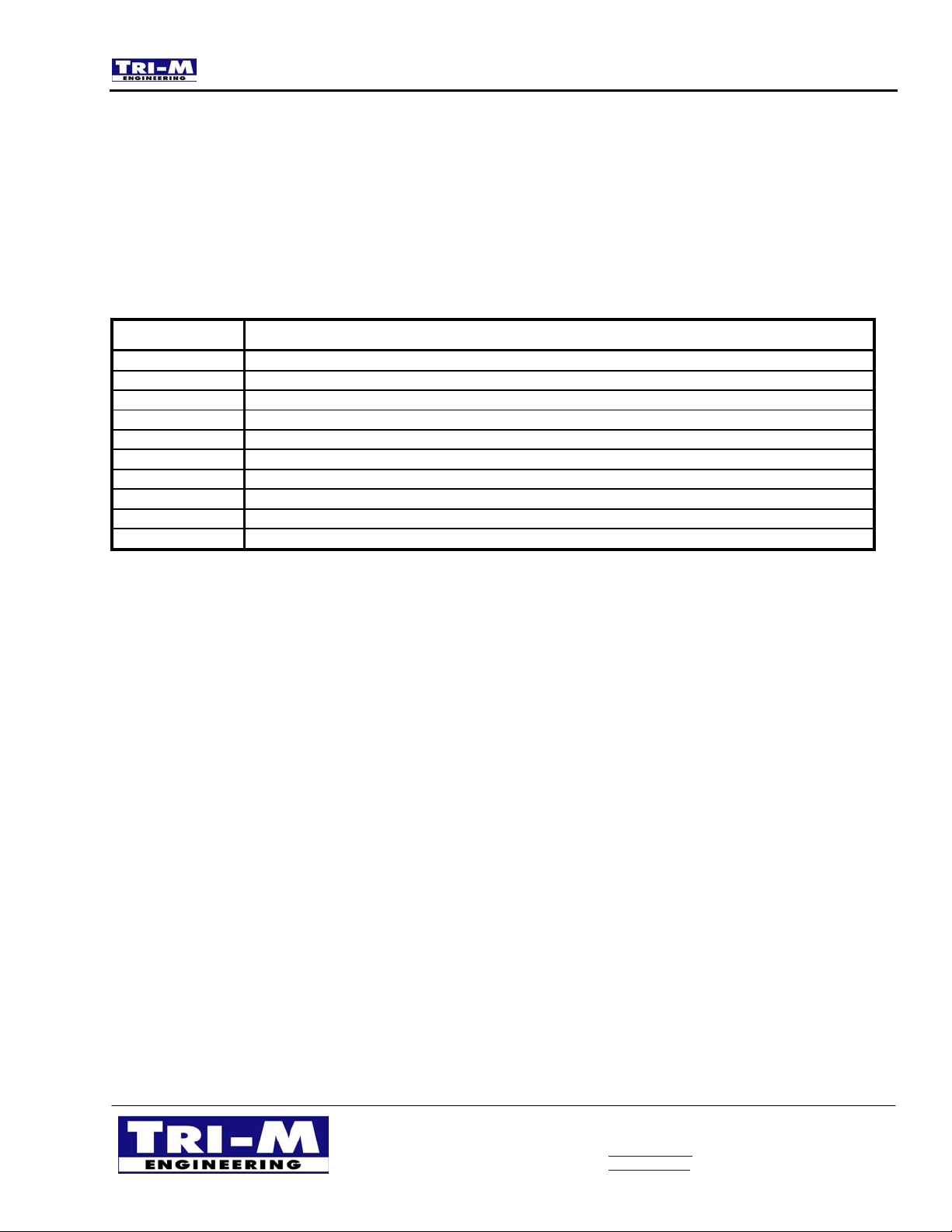
Jumpers on the MZ-6SER are provided to configure the board for different functionality.
Table 1: Jumper List
Label Function
JP1
JP2
JP3
JP4
JP5
JP6
JP7
JP8
JP9
JP10
CPU CLOCK MULTIPLIER & PCI CLOCK DIVIDE
BIOS WRITE ENABLE
WATCH DOG SOURCE
COMPACT FLASH MASTER/SLAVE SELECT
CPU OSCILLATOR SELECT
CORE VOLTAGE SELECT
RS232 COM5 & 6 ENABLE
RS485 HALF/FULL DUPLEX SELECT
MILLENIUM PLUS DOC WRITE ENABLE
BUR/BOOT ROM SELECT
Tri-M Engineering Tel: 800.665.5600, 604.945.9565
1407 Kebet Way, Unit 100 Fax: 604.945.9566
Port Coquitlam, BC V3C 6L3 E-mail: [email protected]
Canada Web site: www.tri-m.com
7
Page 10
24/04/2003 MZ-6SER Manual
J
JP10
Figure 1: Connector and Jumper Location MZ-6SER Top
JP1
CN16
CN14
CN15
CN1 & CN2
CN3 & CN4
CN5 & CN6
JP7
CN13
CN12
P4
JP6
CN7
JP8
Tri-M Engineering Tel: 800.665.5600, 604.945.9565
1407 Kebet Way, Unit 100 Fax: 604.945.9566
Port Coquitlam, BC V3C 6L3 E-mail: [email protected]
Canada Web site: www.tri-m.com
CN8 CN9
CN11
8
Page 11
24/04/2003 MZ-6SER Manual
Figure 2: Connector Location MZ-6SER Bottom
CN10 CN18 CN17
Tri-M Engineering Tel: 800.665.5600, 604.945.9565
1407 Kebet Way, Unit 100 Fax: 604.945.9566
Port Coquitlam, BC V3C 6L3 E-mail: [email protected]
Canada Web site: www.tri-m.com
9
Page 12
24/04/2003 MZ-6SER Manual
CHAPTER 3: JUMPERS
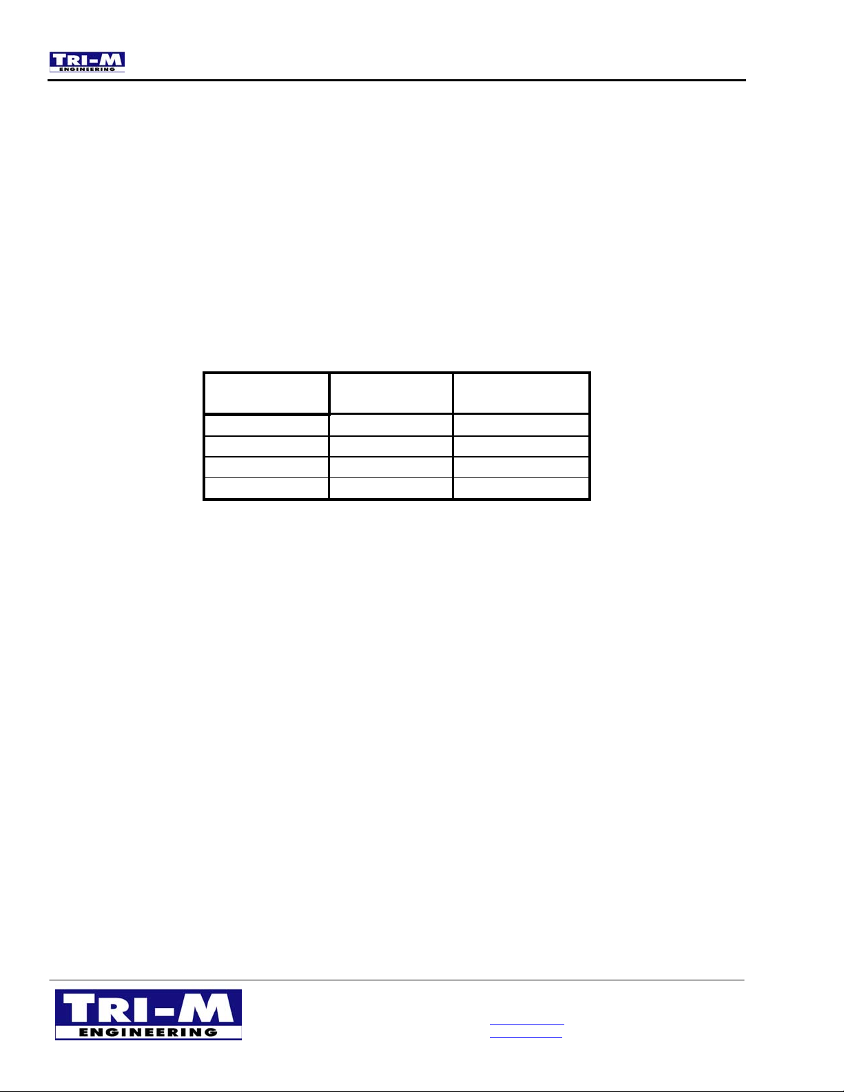
3.1 Clock Multiplier select (JP1)
The clock multiplier selection jumper sets the clock frequency multiplier for the MZ-6SER core.
Each setting will put the MZ-6SER core at a different operating speed.
The CPU operating speed is determined by the CPU clock (33MHz or 64MHz) multiplied by
the CPU frequency ratio.
- Refer to section 3.6 for setting CPU clock
- For example, using 2X ratio, the CPU speed will be (2x64) = 128 MHz
Table 2: Clock Multiplier Select (JP1)
Jumper
CPU Freq ratio
1X
2X
3X**
4X**
*Factory default setting
**The maximum rated speed of the ZFx86 processor is 128MHz. Avoid
using combinations of CPU Freq ratio and Oscillator frequency that results
in over clocking the ZFx86. Over clocking will void the warranty.
JP1 [3-4] JP1 [1-2]
ON* ON*
OFF ON
OFF OFF
ON OFF
Tri-M Engineering Tel: 800.665.5600, 604.945.9565
1407 Kebet Way, Unit 100 Fax: 604.945.9566
Port Coquitlam, BC V3C 6L3 E-mail: [email protected]
Canada Web site: www.tri-m.com
10
Page 13
24/04/2003 MZ-6SER Manual
3.2 PCI Clock Divider (JP1)
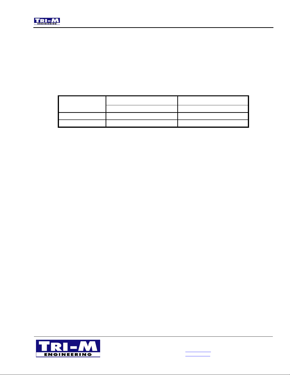
When the CPU oscillator is set for 33 MHz, set the PCI dividers for divide-by-one for proper
operation. When the CPU oscillator is set for 64 MHz, set the PCI Clock dividers for divide-bytwo operation.
- Refer to section 3.6 for setting CPU clock
Table 3: PCI Clock Divider (JP1)
Front side PCI divider Back side PCI dividerFunction
description
Divide by one
Divide by two
JP1 [5-6] JP1 [7-8]
Off Off
On* On*
*Factory default setting
3.3 Write Enable Jumper for Bios Flash (JP2)
Install jumper shunt on JP2 to enable writing to the Bios Flash chip. The Bios chip is a
512Kbyte device with the Bios located at 40000H to 7FFFFH. Locations from 0 to 3FFFFH are
available for the customers use.
- Remove the jumper shunt on JP2 to write protect the Bios Flash. This will allow
read only accesses.
3.4 Watchdog Timer (JP3)
The MZ-6SER has two watchdog timers, WD1 and WD2. Both timers are programmable.
WD1 counter expires in 2 seconds and WD2 in 7ms. WD2 starts counting down after WD1
expires. When WD2 counter reaches zero, it will unconditionally cause a system reset.
The watchdog timer alarms if not triggered by the system or application at least once every 2
seconds. If the watchdog timer does not receive a reset “tickle” when 2 seconds has elapsed,
it generates an alarm signal. The watchdog timer alarm is reset “tickled” by toggling the WDI
signal or writing to index 0x10h of the ZF-Logic I/O space. The watchdog is triggered
continuously (disabled) if jumper shunt JP3 [2-3] is installed. This arrangement allows
watchdog input (WDI) to be toggled by the watchdog alarm output (WDO) in a self-triggering
fashion. If a jumper shunt JP3 [1-2] is installed, the watchdog will be triggered by an external
signal or event from pin5 of CN8.
The watchdog timer alarm signal (WDO) can be programmed to generate the following
response when the corresponding bit is set at the watchdog control register in the ZF-Logic I/O
space.
• Non-maskable interrupt (NMI)
Tri-M Engineering Tel: 800.665.5600, 604.945.9565
1407 Kebet Way, Unit 100 Fax: 604.945.9566
Port Coquitlam, BC V3C 6L3 E-mail: [email protected]
Canada Web site: www.tri-m.com
11
Page 14
24/04/2003 MZ-6SER Manual
• System controller interrupt (SCI)
• System Management interrupt (SMI)
• Hardware reset
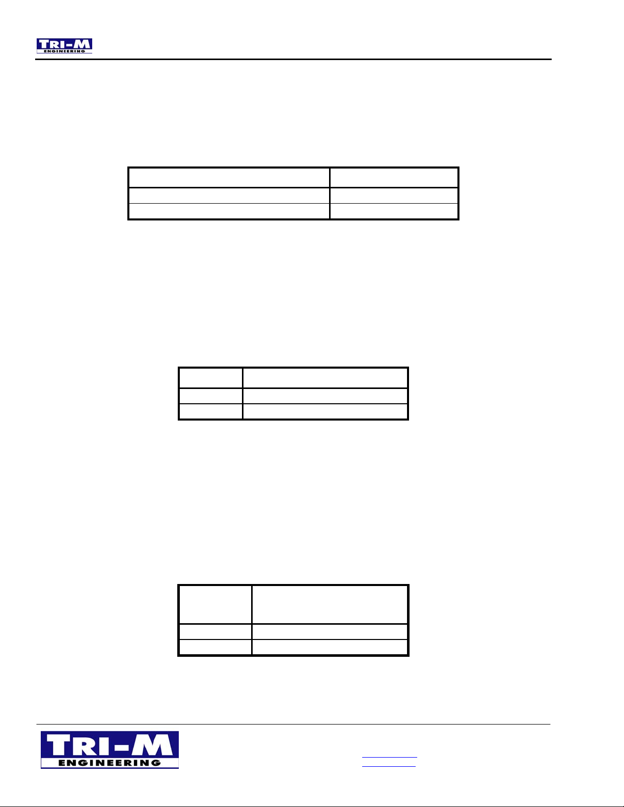
Table 4: Watchdog Jumper (CN16)
Function Jumper Position
External source to reset watchdog
Disable watchdog
1-2
2-3
Note: The watchdog timer is not enabled at power up by the BIOS. Therefore, the
position of the jumper at CN16 does not affect the operation of the MZ-6SER.
3.5 Master /Slave Mode Select (JP4)
JP4 configures the compact flash device inserted into CN18 either as a master or slave IDE
device.
Table 5: Master/Slave Mode Select (JP4)
Mode
Master
Slave
JP4
Off*
On
*Factory default setting
3.6 CPU Clock Oscillator Select (JP5)
The CPU clock oscillator can be set for 33 MHz or 64 MHz operation. Selecting the 33MHz
oscillator and setting the clock multiplier to 1X will offer the lowest power consumption, while
setting the CPU clock oscillator to 64 MHz and the clock multiplier to 2X will offer the greatest
processing capability.
Table 6: CPU Clock select (JP5)
Oscillator
JP5
Frequency
33 MHz
64 MHz
JP5 [2-3] shunt On
JP5 [1-2] shunt On*
*Factory default setting
**The MZ-6SER will not function without a shunt installed on JP5
Tri-M Engineering Tel: 800.665.5600, 604.945.9565
1407 Kebet Way, Unit 100 Fax: 604.945.9566
Port Coquitlam, BC V3C 6L3 E-mail: [email protected]
Canada Web site: www.tri-m.com
12
Page 15
24/04/2003 MZ-6SER Manual
3.7 CPU Core Voltage Select (JP6)
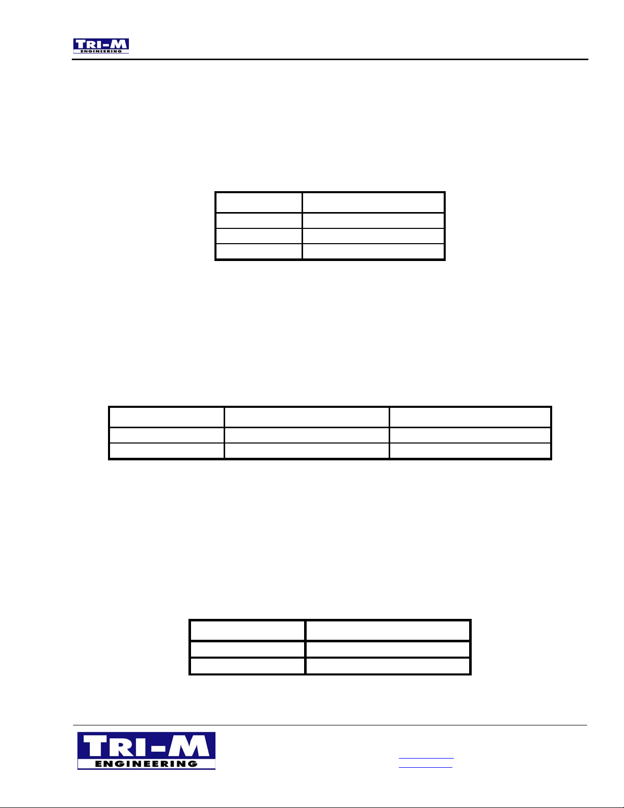
At a CPU speed of 128 MHz, the core voltage must be set for 2.75 volts. At frequencies below
128 MHz, the core voltage should be lowered to conserve power, and to reduce the dissipated
heat. Jumper JP6 allows for three possible core voltages of 2.75 volts, 2.5 volts and 2.25
volts.
Table 7: CPU Core Voltage Select (JP6)
Core Voltage JP6
2.25 volts
2.5 volts
2.75 volts
JP6 [2-3] shunt On
JP6 [1-2] shunt On*
No shunt installed
*Factory default setting
3.8 Enable RS232 Drivers for Serial 5 and Serial 6 Port (JP7)
When using serial five in half duplex RS485 mode, the serial five RS232 driver must be
disabled. When using serial six for half or full duplex RS485 mode, the serial six RS232 driver
must be disabled.
Table 8: Serial 5 and 6 RS232 Driver Disable (JP7)
Serial 5 RS232 Driver Serial 6 RS232 Driver
Driver Enable
Driver Disable
JP7 [1-3]* JP7 [2-4]*
JP7 [3-5] JP7 [4-6]
*Factory default setting
3.9 RS485 Half/Full Duplex Mode Select (JP8)
Jumper JP8 routes the RS485 signals to setup half or full duplex operation. When half duplex
operation is setup, communication for the RS485 port five is routed to serial ports five, and
communication for the RS485 ports six is routed to serial port six. When full duplex mode is
selected the RS485 receive signal is routed to the RS485 port six.
Table 9: Half/Full Duplex Routing (JP8)
Installed Jumpers
Half Duplex
Full Duplex
Tri-M Engineering Tel: 800.665.5600, 604.945.9565
1407 Kebet Way, Unit 100 Fax: 604.945.9566
Port Coquitlam, BC V3C 6L3 E-mail: [email protected]
Canada Web site: www.tri-m.com
JP8 [1-3] [5-7] [6-8]
JP8 [3-4] [7-8]
13
Page 16
24/04/2003 MZ-6SER Manual
3.10 M-Systems Millennium Plus Disk-On-Chip Write Enable (JP9) - (Only for the MZ6SER-MP version)
Install jumper shunt on JP9 to enable writing to the Millennium Plus. The Millennium Plus chip
is a 32Mbyte solid-state disk. Please refer to the M-Systems manual on the Millennium Plus
for setup, configuration and programming.
Remove the jumper shunt on JP9 to write protect the Millennium Plus. This will allow read only
accesses.
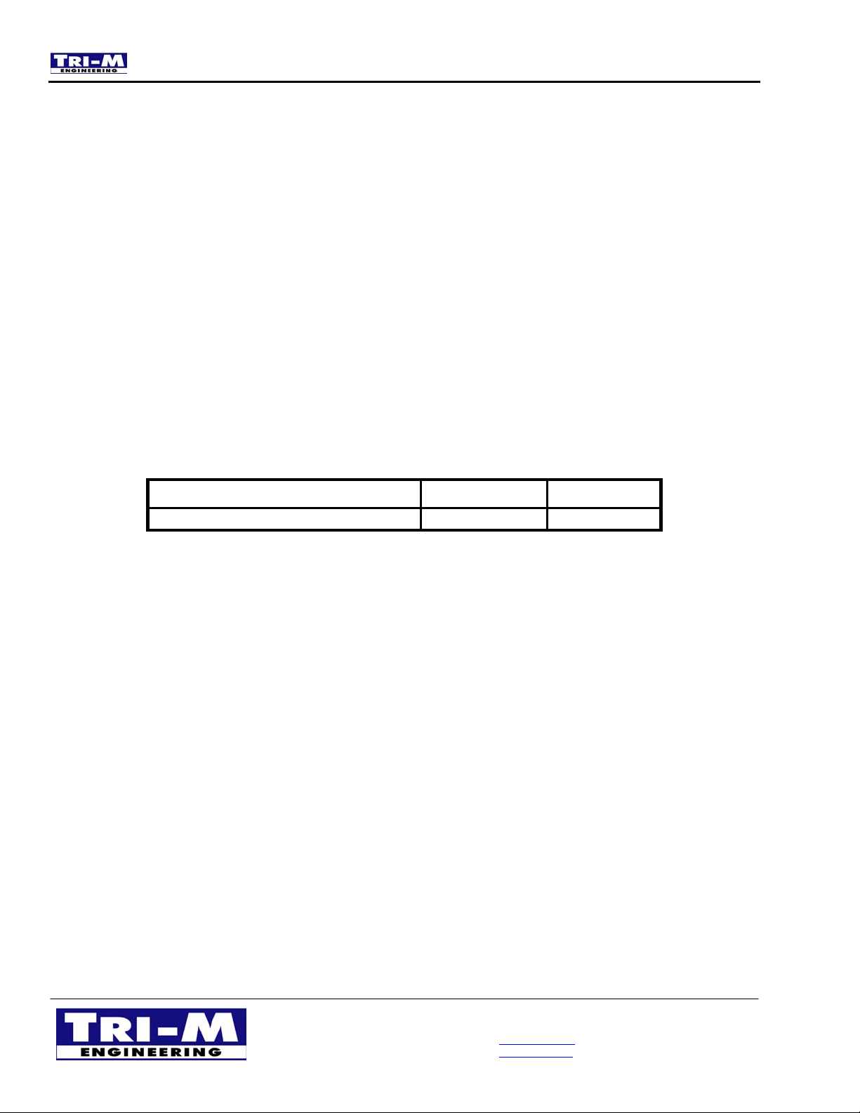
3.11 BUR/Boot ROM Select (JP10)
JP10 allows the MZ-6SER to boot from standard BIOS or BUR. If boot ROM mode is selected,
the MZ-6SER will startup normally by executing the BIOS code and transfer control to a boot
device. If BUR mode is selected, the MZ-6SER will execute the BUR code to update the flash
BIOS using the Z-Tag interface. It also provides an elementary debugger console functionality
through COM1. For details of Z-Tag and BUR operation, see the MachZ data book.
Table 10: Bur/Boot Rom Select (JP10)
BUR/BOOT select BUR Mode Boot ROM
JP10
*Factory setting
OFF ON*
Tri-M Engineering Tel: 800.665.5600, 604.945.9565
1407 Kebet Way, Unit 100 Fax: 604.945.9566
Port Coquitlam, BC V3C 6L3 E-mail: [email protected]
Canada Web site: www.tri-m.com
14
Page 17
24/04/2003 MZ-6SER Manual
CHAPTER 4: CONNECTORS
Connectors on the MZ-6SER are provided to interface to external devices such as hard disk
drives, floppy drives and keyboards. Pin 1 of each connector on the MZ-6SER should line up
with Pin 1 of the corresponding mating connector on the cable.
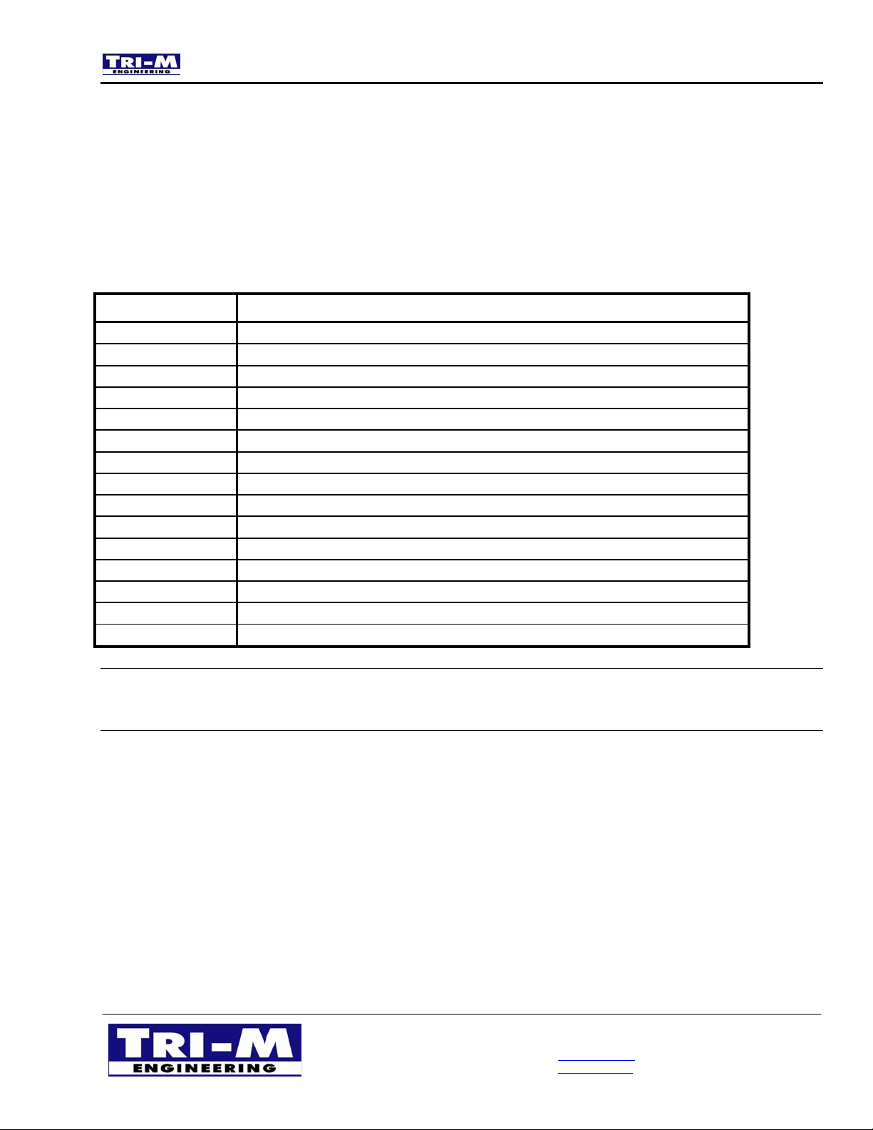
Table 11: MZ-6SER Connector List
Connector Function
CN1 & 2
CN3 & 4
CN5 & 6
CN7
CN8
CN9
CN10
CN11
CN12
CN13
CN14
CN15
CN16
CN17
CN18
RS232 COM1 & 2 connector
RS232 COM 3 & 4 connector
RS232 COM 5 & 6 connector
RS485 COM5 & 6
Utility (keyboard, mouse, speaker)
Floppy interface connector
Z-Tag interface
USB 1 &2 connector
IDE interface connector
Parallel connector
PC 104 connector (40 pin)
PC 104 connector (64 pin)
Main power input connector
CMOS backup battery holder
Compact flash connector
Note: Pin-1 of each connector on the MZ-6SER is designated by a small white dot on the
PCB. Pin-1 on the connector should line up with pin-1 of the corresponding mating connector
on the cable.
4.1 Serial Interfaces (CN1 to CN6)
The MZ-6SER provides six PC-compatible asynchronous serial ports. All six serial ports have
RS232 drivers. Serial port five and serial port six are jumper configurable as half duplex
RS485 ports. Serial port six can be configured as a full duplex RS485 (with serial port five in
RS232 mode only). Serial RS232 ports connectors are grouped in sets of two. That is, Serial
1 (CN1) and Serial 2 (CN2) connectors are adjacent to each other creating a 10 pin by 2 pin
header. Similarly, serial 3 (CN3) and serial 4 (CN4) are adjacent, and serial 5 (CN5) and serial
6 (CN6) are adjacent. RS485 signals are available on connector CN7.
All six serial ports supply full complements of input and output handshaking lines. These
signals are at standard RS232C levels. The RS232C level converters provide the required
RS232C voltage levels with internal +5 volt to ±9 volt converters. The serial port drivers have
Tri-M Engineering Tel: 800.665.5600, 604.945.9565
1407 Kebet Way, Unit 100 Fax: 604.945.9566
Port Coquitlam, BC V3C 6L3 E-mail: [email protected]
Canada Web site: www.tri-m.com
15
Page 18
24/04/2003 MZ-6SER Manual
an automatic power down mode that turns off the driver outputs. This occurs whenever there
isn't a valid signal level on any of the receive pins on the driver chip.
Serial port one and Serial port two can be disabled using BIOS SETUP. The IOCS (I/O chip
select) signals the quad UART uses for Serial ports 3 to 6 can be disabled through the BIOS
SETUP. When disabled, the port’s I/O address is made available for other expansion devices
on the 16-bit BUS.
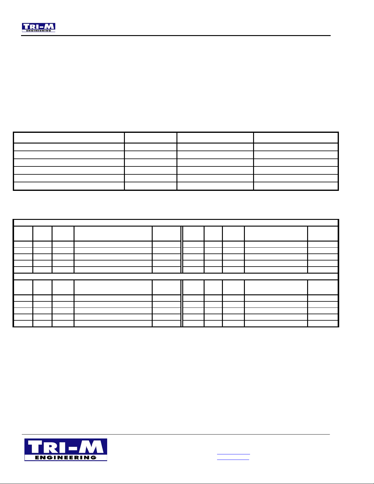
Table 12: Serial Port Resources
Serial Port Typical Usage I/O Address Standard Interrupt
Serial 1 (CN1)
Serial 2 (CN2)
Serial 3 (CN3)
Serial 4 (CN4)
Serial 5 (CN5)
Serial 6 (CN6)
COM1 3F8h–3FFh IRQ4
COM2 2F8h–2FFh IRQ3
COM3 3E8h–3EFh IRQ5
COM4 2E8h–2EFh IRQ10
COM5 2E0h–2E8h IRQ11
COM6 2F0h–2F8h IRQ15
CN1
1
3
5
7
9
CN2
1
3
5
7
9
Table 13: RS232 Serial Ports Com1 (CN1) and Com2 (CN2)
Serial Port COM1 Connector (CN1)
DB-9
DB-9
Signal Function In/Out CN1
1
Pin
1 DCD1 Serial 1 Data Carrier Detect INPUT
2 RXD1 Serial 1 Receive Data INPUT
3 TXD1 Serial 1 Transmit Data OUTPUT
4 DTR1 Serial 1 Data Terminal Ready OUTPUT
5 GND Signal Ground
Serial Port COM2 Connector (CN2)
Signal Function In/Out CN2
1
Pin
1 DCD2 Serial 2 Data Carrier Detect INPUT
2 RXD2 Serial 2 Receive Data INPUT
3 TXD2 Serial 2 Transmit Data OUTPUT
4 DTR2 Serial 2 Data Terminal Ready OUTPUT
5 GND Signal Ground
Table 14: RS232 Serial Ports Com3 (CN3) and Com4 (CN4)
10
10
DB-9
2
4
6
8
DB-9
2
4
6
8
Signal Function In/Out
1
Pin
6 DSR1 Serial 1 Data Set Ready INPUT
7 RTS1 Serial 1 Request To Send OUTPUT
8 CTS1 Serial 1 Clear To Send INPUT
9 RI1 Serial 1 Ring Indicator INPUT
N/C No connection
Signal Function In/Out
1
Pin
6 DSR2 Serial 2 Data Set Ready INPUT
7 RTS2 Serial 2 Request To Send OUTPUT
8 CTS2 Serial 2 Clear To Send INPUT
9 RI2 Serial 2 Ring Indicator INPUT
N/C No connection
Tri-M Engineering Tel: 800.665.5600, 604.945.9565
1407 Kebet Way, Unit 100 Fax: 604.945.9566
Port Coquitlam, BC V3C 6L3 E-mail: [email protected]
Canada Web site: www.tri-m.com
16
Page 19
24/04/2003 MZ-6SER Manual
Serial Port COM3 Connector (CN3)
CN3
1
3
5
7
9
CN4
1
3
5
7
9
DB-9
Pin
DB-9
Pin
Signal Function In/Out CN3
1
1 DCD3 Serial 3 Data Carrier Detect INPUT
2 RXD3 Serial 3 Receive Data INPUT
3 TXD3 Serial 3 Transmit Data OUTPUT
4 DTR3 Serial 3 Data Terminal Ready OUTPUT
5 GND Signal Ground
Serial Port COM4 Connector (CN4)
Signal Function In/Out CN4
1
1 DCD4 Serial 4 Data Carrier Detect INPUT
2 RXD4 Serial 4 Receive Data INPUT
3 TXD4 Serial 4 Transmit Data OUTPUT
4 DTR4 Serial 4 Data Terminal Ready OUTPUT
5 GND Signal Ground
10
10
DB-9
2
4
6
8
DB-9
2
4
6
8
Signal Function In/Out
1
Pin
6 DSR3 Serial 3 Data Set Ready INPUT
7 RTS3 Serial 3 Request To Send OUTPUT
8 CTS3 Serial 3 Clear To Send INPUT
9 RI3 Serial 3 Ring Indicator INPUT
N/C No connection
Signal Function In/Out
1
Pin
6 DSR4 Serial 4 Data Set Ready INPUT
7 RTS4 Serial 4 Request To Send OUTPUT
8 CTS4 Serial 4 Clear To Send INPUT
9 RI4 Serial 4 Ring Indicator INPUT
N/C No connection
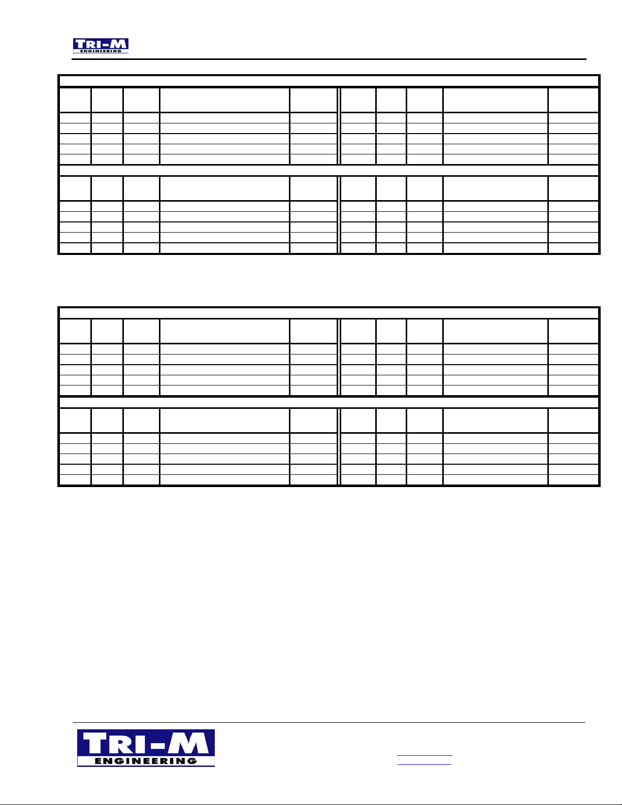
Table 15: RS232 Serial Ports Com5 (CN5) and Com6 (CN6)
Serial Port COM5 Connector (CN5)
CN5
CN6
DB-9
Pin
1
3
5
7
9
DB-9
Pin
1
3
5
7
9
1
References to DB-9 connectors are for cross-reference only since they are not present on the
Signal Function In/Out CN5
1
1 DCD5 Serial 5 Data Carrier Detect INPUT
2 RXD5 Serial 5 Receive Data INPUT
3 TXD5 Serial 5 Transmit Data OUTPUT
4 DTR5 Serial 5 Data Terminal Ready OUTPUT
5 GND Signal Ground
Serial Port COM6 Connector (CN6)
Signal Function In/Out CN6
1
1 DCD6 Serial 6Data Carrier Detect INPUT
2 RXD6 Serial 6 Receive Data INPUT
3 TXD6 Serial 6 Transmit Data OUTPUT
4 DTR6 Serial 6 Data Terminal Ready OUTPUT
5 GND Signal Ground
10
10
DB-9
2
4
6
8
DB-9
2
4
6
8
Signal Function In/Out
1
Pin
6 DSR5 Serial 5 Data Set Ready INPUT
7 RTS5 Serial 5 Request To Send OUTPUT
8 CTS5 Serial 5 Clear To Send INPUT
9 RI5 Serial 5 Ring Indicator INPUT
N/C No connection
Signal Function In/Out
1
Pin
6 DSR6 Serial 6 Data Set Ready INPUT
7 RTS6 Serial 6 Request To Send OUTPUT
8 CTS6 Serial 6 Clear To Send INPUT
9 RI6 Serial 6 Ring Indicator INPUT
N/C No connection
MZ-6SER but only at the end of an attached cable. The connector description of DB-9 is used
in this manual for clarity even though the correct technical term is DE-9. The second letter of
DE-9 designates the shell size (per EIA standard). However, the majority of the world
recognizes the description of DB-9 and not DE-9.
2
CN1 to CN6 are edge mounted PCB connectors with even number pins located on the “top”,
and odd number pins on the “bottom”.
Tri-M Engineering Tel: 800.665.5600, 604.945.9565
1407 Kebet Way, Unit 100 Fax: 604.945.9566
Port Coquitlam, BC V3C 6L3 E-mail: [email protected]
Canada Web site: www.tri-m.com
17
Page 20
24/04/2003 MZ-6SER Manual
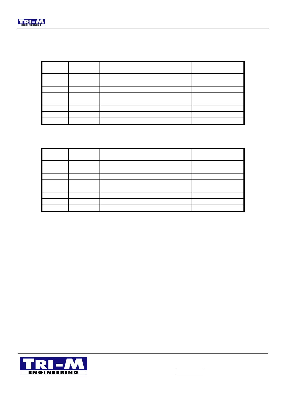
Table 16: RS485 Serial Connector (CN7) for Half Duplex Mode
Pin# Signal Function Input/Output
1
2
3
4
5
6
7
8
TR1A 100 ohm termination resistor 1 N/A
TR1B 100 ohm termination resistor 1 N/A
CMD6+ Serial 6 RS-422 Data + Input/Output
CMD6- Serial 6 RS-422 Data - Input/Output
TR2A 100 ohm termination resistor 2 N/A
TR2B 100 ohm termination resistor 2 N/A
CMD5+ Serial 5 RS-422 Data + Input/Output
CMD5- Serial 5 RS-422 Data - Input/Output
Table 17: RS485 Serial Connector (CN7) for Full Duplex Mode
Pin# Signal Function Input/Output
1
2
3
4
5
6
7
8
2
CN7 is edge mounted PCB connectors with even number pins located on the “top”, and odd
TR1A 100 ohm termination resistor 1 N/A
TR1B 100 ohm termination resistor 1 N/A
CMD6+ Serial 6 RS-422 Transmit Data + Output
CMD6- Serial 6 RS-422 Transmit Data - Output
TR2A 100 ohm termination resistor 2 N/A
TR2B 100 ohm termination resistor 2 N/A
CMD6+ Serial 6 RS-422 Receive Data + Input
CMD6- Serial 6 RS-422 Receive Data - Input
number pins on the “bottom”.
Tri-M Engineering Tel: 800.665.5600, 604.945.9565
1407 Kebet Way, Unit 100 Fax: 604.945.9566
Port Coquitlam, BC V3C 6L3 E-mail: [email protected]
Canada Web site: www.tri-m.com
18
Page 21
24/04/2003 MZ-6SER Manual
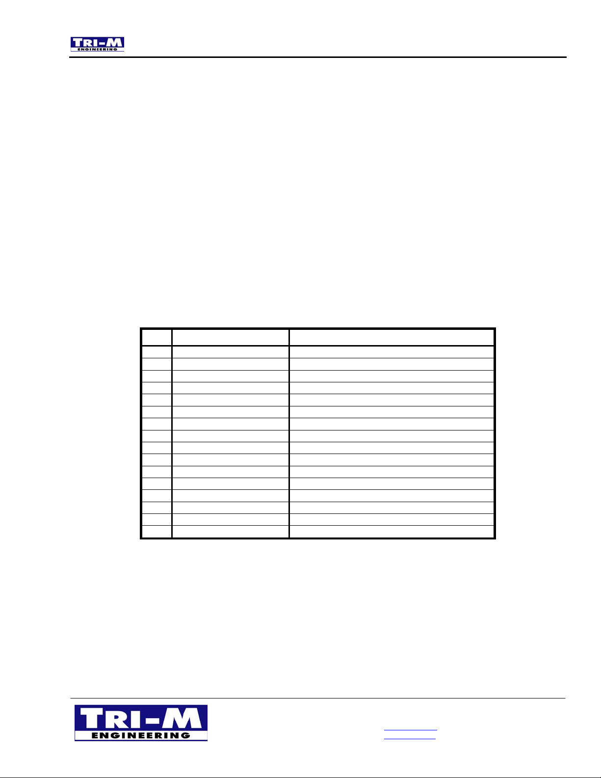
4.2 Utility Connector (CN8)
The following inputs and outputs on are provided on a flat ribbon connector:
• Keyboard input
• PS/2 mouse input
• Infrared I/O
• Speaker Out
• SMBus/I2C
• RTC & CMOS backup battery
• Watchdog trigger source
• Hardware reset
• Hard drive LED
The MZ104+UTIL card supports the flat ribbon cable from the MZ-6SER card. This provides
an easy and quick method to connect to the external "utility" devices to the
MZ-6SER.
Table 18: Utility connector (CN8)
Pin Signal Function
HDDLEDOUT Hard drive LED output (8mA source)
1
RESETX Hardware reset
2
IRRXD Infrared receive
3
IRTXD Infrared Transmit
4
WD_EXT External Trigger Source for watchdog timer
5
VBAT_CLK RTC backup battery +V terminal (3.6V)
6
SDA SMBus data
7
KBMPWR +5V
8
GND Ground
9
SCL SMBus clock
10
SPKOUT Speaker output
11
KBLOCKX Keyboard lock
12
MCLKX P/S2 mouse clock
13
MDATX P/S2 mouse data
14
KBCLKX Keyboard clock
15
KBDATX Keyboard data
16
Tri-M Engineering Tel: 800.665.5600, 604.945.9565
1407 Kebet Way, Unit 100 Fax: 604.945.9566
Port Coquitlam, BC V3C 6L3 E-mail: [email protected]
Canada Web site: www.tri-m.com
19
Page 22
24/04/2003 MZ-6SER Manual
4.3 Floppy Interface (CN9)
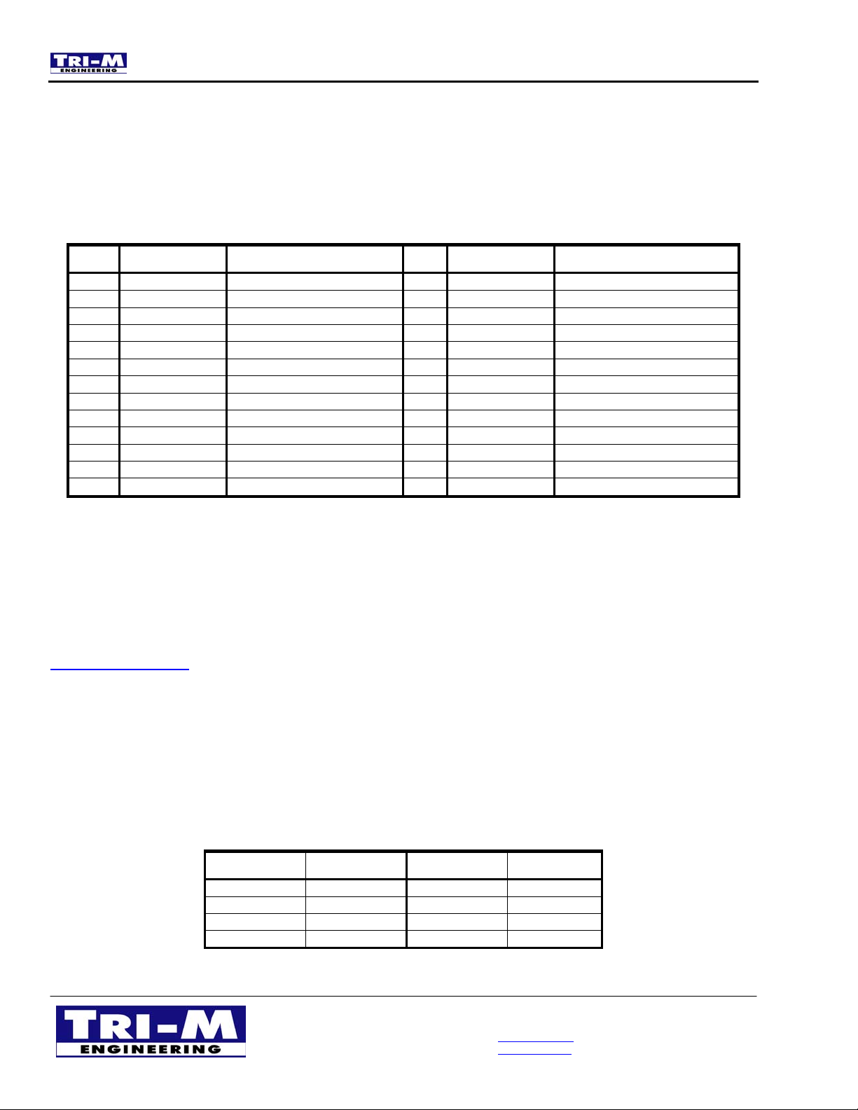
The floppy interface uses a flat ribbon cable connector to provide the signals to control one
3½“ or 5¼” floppy drive. The default interrupt request for the floppy interface is IRQ6.
Table 19: Floppy Interface (CN9)
Pin Signal Function Pin Signal Function
VCC5V +5V
1
VCC5V +5V
3
VCC5V +5V
5
NC -
7
NC -
9
NC -
11
NC -
13
GND Ground
15
GND Ground
17
GND Ground
19
GND Ground
21
GND Ground
23
GND Ground
25
INDX Index
2
DRX0 Drive select 0
4
DSKCHGX Disk Change
6
NC -
8
MTRXO Motor On
10
DIRX Direction Select
12
STEPX Step
14
WDATAX Write data
16
WGATEX Write gate
18
TRKX0 Track 00
20
WPX Write Protect
22
RDATAX Read data
24
HDSELX Side one select
26
4.4 Z-Tag connector (CN10)
The Z-Tag connector (CN10) is a 14-pin edge connector that interfaces with the Z-Tag Dongle
allowing for easy field flash updates or user code execution. Please refer to the Z-Tag and
BUR chapter of the ZFx86 Data Book for complete details. A Z-Tag Manager utility program
and manual are provided on the MZ104+ Quickstart CD and are available for download at
www.ZFMicro.com. The Z-Tag Dongle, part number ZFx86DONGLE-1, is available from Tri-M
Systems.
4.5 USB 1,2 Connector (CN11)
The MZ-6SER provides two USB (Universal Serial BUS) interfaces, which give complete plug
and play, for external devices.
Table 20: USB 1,2 Connector (CN11)
Pin Signal Pin Signal
1 USBVCC2 2 USBD2F3 USBD2F+ 4 GND
5 USBVCC1 6 USBD1F-
1
CN11 is an edge mounted PCB connector with odd number pins located on the “top”, and
7 USBD1F+ 8 GND
even number pins on the “bottom”.
Tri-M Engineering Tel: 800.665.5600, 604.945.9565
1407 Kebet Way, Unit 100 Fax: 604.945.9566
Port Coquitlam, BC V3C 6L3 E-mail: [email protected]
Canada Web site: www.tri-m.com
20
Page 23
24/04/2003 MZ-6SER Manual
4.6 IDE Interface (CN12)
The MZ-6SER has a PCI bus mastering ATA-4 compatible IDE controller. The IDE controller
supports Ultra DMA, Multi-word DMA, and all Programmed I/O (PIO) modes. Up to two drives
can be connected, in a master-slave arrangement. Generally, the first hard disk drive (master)
will appear as C drive. The second drive, if attached, will appear as D.
Table 21: Hard Disk Resources
Resource Function
I/O Address (1F0h-1F7h) Hard Disk Interface
IRQ14 Interrupt
Use SETUP to auto-detect your attached hard drives. For further details about setting up IDE
hard disk parameters See the SETUP description in the BIOS manual provided on the MZ104
Quickstart CD or available for download at www.ZFMicro.com.
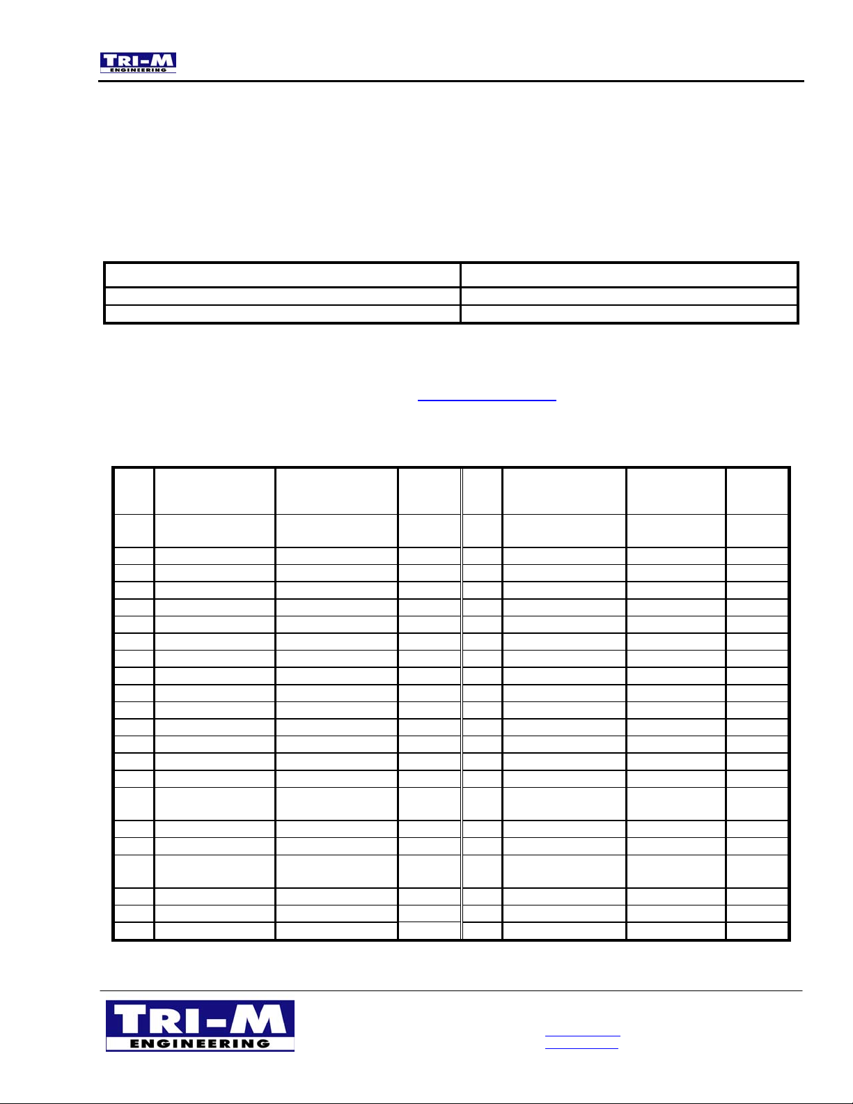
Table 22: IDE Drive Interface (CN12)
Pin Signal Name Function
1
3
5
7
9
11
13
15
17
19
21
23
25
27
29
31
33
35
37
39
41
43
1
CN12 is an edge mounted PCB connector with odd number pins located on the “top”, and
RESET Reset signal from
host
DD7 Data bit 7 I/O
DD6 Data bit 6 I/O
DD5 Data bit 5 I/O
DD4 Data bit 4 I/O
DD3 Data bit 3 I/O
DD2 Data bit 2 I/O
DD1 Data bit 1 I/O
DD0 Data bit 0 I/O
GND Ground GND
DREQ DMA 0 Request OUT
DIOW Write strobe OUT
DIOR Read strobe OUT
IORDY I/O channel ready IN
IDEPDACK DMA 0 Acknowledge IN
IRQ14 Drive interrupt
request
DA1 IDE Address 1 Out
DA0 IDE Address 1 Out
HDCS0 IDE Chip Select 0 Out
HDDLED Drive Activity Out
VCC5V +5V +5V
GND Ground GND
In/Ou
t
OUT
IN
Pin Signal Name Function
2
4
6
8
10
12
14
16
18
20
22
24
26
28
30
32
34
36
38
40
42
44
GND Ground GND
DD8 Data bit 8 I/O
DD9 Data bit 9 I/O
DD10 Data bit 10 I/O
DD11 Data bit 11 I/O
DD12 Data bit 12 I/O
DD13 Data bit 13 I/O
DD14 Data bit 14 I/O
DD15 Data bit 15 I/O
KEY Keyed pin N/C
GND Ground GND
GND Ground GND
GND Ground GND
GND Ground OUT
GND Ground GND
IOCS16 I/O Chip Select
16
RSVD Reserved N/C
DA2 IDE Address 2 Out
HDCS1 IDE Chip Select
1
GND Ground GND
VCC5V +5V +5V
NC - NC
In/Ou
t
even number pins on the “bottom”.
In
Out
Tri-M Engineering Tel: 800.665.5600, 604.945.9565
1407 Kebet Way, Unit 100 Fax: 604.945.9566
Port Coquitlam, BC V3C 6L3 E-mail: [email protected]
Canada Web site: www.tri-m.com
21
Page 24
24/04/2003 MZ-6SER Manual
4.7 Parallel (CN13)
The MZ-6SER parallel port is fully compatible with the PC/AT parallel port. In the extended
mode, it functions as a PS/2-like bi-directional port. In Extended Capabilities Port (ECP) mode,
it is IEEE 1284 compliant, including level 2.
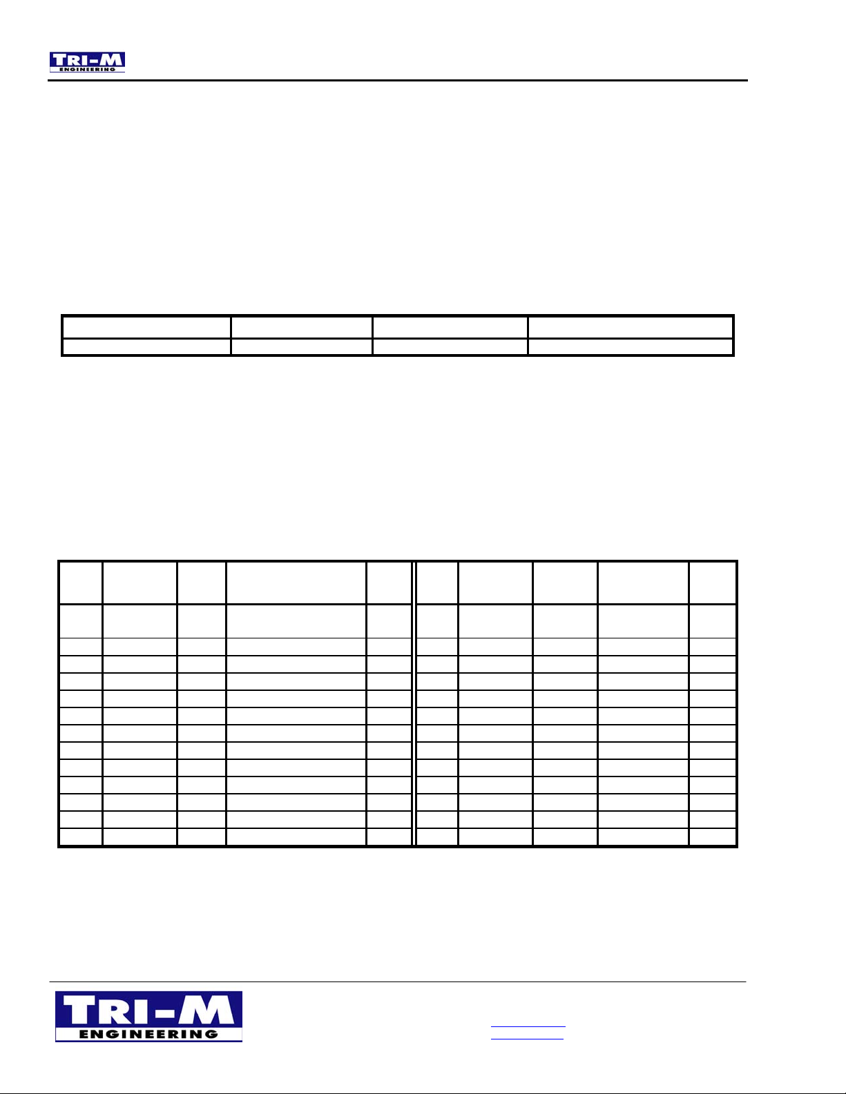
The parallel ports uses the following PC resources when enabled:
Table 23: Parallel Port Resources
Parallel Port Typical Usage I/O Address Standard Interrupt
Parallel 1 LPT1 378H – 37Fh IRQ7
The default interrupt for parallel port LPT1 is IRQ7. The parallel port output signals provide up
to 14-mA drive current. RC filters are provided for noise suppression. The parallel port signals
appear on CN13, a dual-row ribbon-cable pin edge connector. The port may be cabled to
appear on a standard PC DB-25 connector. A DB-25 connector and cable are provided for this
purpose in the optional MZ-6SER cable kit. The following table shows the parallel port signals
appearing on CN13 and the equivalent pin out on a DB-25 connector.
Table 24: Parallel Port Connections (CN13)
10
12
14
16
18
20
22
24
26
DB-25
1
Pin
2
4
6
8
14 AUTOFD
15 ERR- Printer error IN
16 INIT- Initialize printer OUT
17 SLCTIN- Selects printer OUT
18 GND Signal Ground N/A
19 GND Signal Ground N/A
20 GND Signal Ground N/A
21 GND Signal Ground N/A
22 GND Signal Ground N/A
23 GND Signal Ground N/A
24 GND Signal Ground N/A
25 GND Signal Ground N/A
N/A GND Signal Ground N/A
Signal Function
Auto feed OUT
-
In/Ou
t
11
13
15
17
19
21
23
25
DB-25
1
Pin
1
3
5
7
9
1 STRB- Output data strobe OUT
2 PD0 Data bit 0 I/O
3 PD1 Data bit 1 I/O
4 PD2 Data bit 2 I/O
5 PD3 Data bit 3 I/O
6 PD4 Data bit 4 I/O
7 PD5 Data bit 5 I/O
8 PD6 Data bit 6 I/O
9 PD7 Data bit 7 I/O
10 ACK- Character acknowledged IN
11 BUSY Printer busy IN
12 PE Out of paper IN
13 SLCT Printer selected IN
Signal Function
CN13
1
References to DB-9 connectors are for cross-reference only since they are not present on the
In/Ou
t
CN13
MZ-6SER but only at the end of an attached cable.
2
CN13 is an edge mounted PCB connector with odd number pins located on the “top”, and
even number pins on the “bottom”.
Tri-M Engineering Tel: 800.665.5600, 604.945.9565
1407 Kebet Way, Unit 100 Fax: 604.945.9566
Port Coquitlam, BC V3C 6L3 E-mail: [email protected]
Canada Web site: www.tri-m.com
22
Page 25
24/04/2003 MZ-6SER Manual
4.8 PC/104 connectors (CN14, AND CN15)
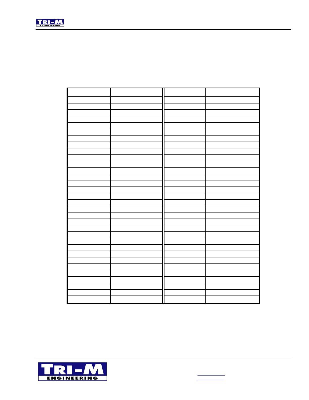
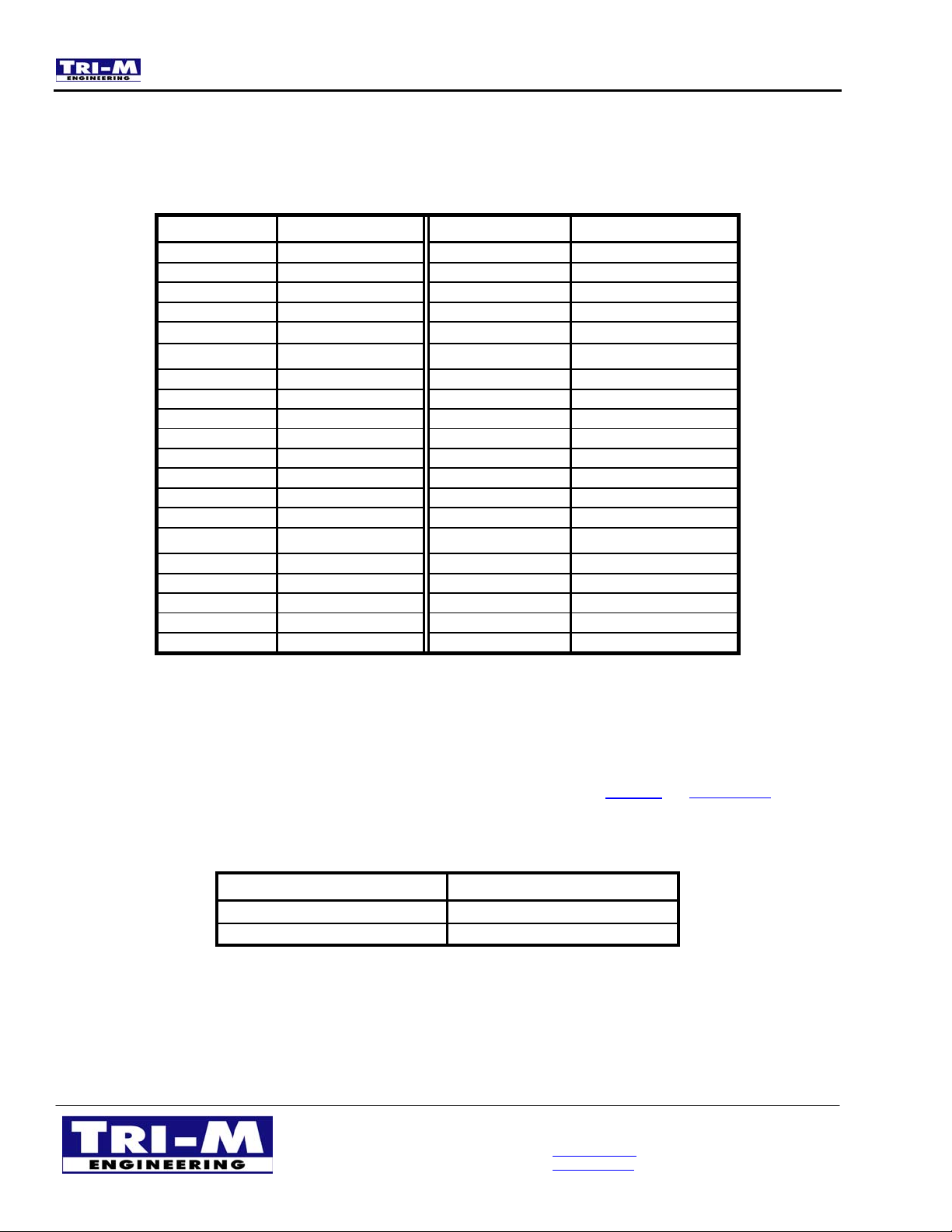
CN14 and CN15 allow PC/104 expansion modules to be added the MZ-6SER. All data,
address and control signals are able to sink 10mA and source 8mA.
Table 25: PC/104 8bit Connector (CN14)
Pin # Signal Pin # Signal
A1
A2
A3
A4
A5
A6
A7
A8
A9
A10
A11
A12
A13
A14
A15
A16
A17
A18
A19
A20
A21
A22
A23
A24
A25
A26
A27
A28
A29
A30
A31
A32
IOCHK
SD7
SD6
SD5
SD4
SD3
SD2
SD1
SD0
IOCHRDY
AEN
SA19
SA18
SA17
SA16
SA15
SA14
SA13
SA12
SA11
SA10
SA9
SA8
SA7
SA6
SA5
SA4
SA3
SA2
SA1
SA0
GND
B1
B2
B3
B4
B5
B6
B7
B8
B9
B10
B11
B12
B13
B14
B15
B16
B17
B18
B19
B20
B21
B22
B23
B24
B25
B26
B27
B28
B29
B30
B31
B32
GND
RSTDRV
+5V
IRQ9
N/A
N/A
-12V
ZEROWS
+12V
KEY
SMEMW
SMEMR
IOW
IOR
N/A
N/A
DACK1
DRQ1
REFRESH
CLK8MHZ
IRQ7
N/A
IRQ5
IRQ4
IRQ3
N/A
TC
BALE
+5V
CLK14MHZ
GND
GND
Tri-M Engineering Tel: 800.665.5600, 604.945.9565
1407 Kebet Way, Unit 100 Fax: 604.945.9566
Port Coquitlam, BC V3C 6L3 E-mail: [email protected]
Canada Web site: www.tri-m.com
23
Page 26
24/04/2003 MZ-6SER Manual
Table 26: PC/104 16bit Connector (CN15)
Pin # Signal Pin # Signal
C0
C1
C2
C3
C4
C5
C6
C7
C8
C9
C10
C11
C12
C13
C14
C15
C16
C17
C18
C19
GND
SBHEX
SA23
SA22
SA21
SA20
SA19
SA18
SA17
MEMR
MEMW
SD8
SD9
SD10
SD11
SD12
SD13
SD14
SD15
KEY
D0
D1
D2
D3
D4
D5
D6
D7
D8
D9
D10
D11
D12
D13
D14
D15
D16
D17
D18
D19
GND
MCS16
IOCS16
IRQ10
IRQ11
IRQ12
IRQ15
N/A
N/A
N/A
DACK5
DRQ5
N/A
N/A
N/A
N/A
+5V
MASTER
GND
GND
4.9 External Power (CN16)
The MZ-6SER can be powered by supplying 5VDC and common to CN4. Alternatively, the
MZ-6SER can be powered by supplying 5VDC through the 16-bit PC104 connector (CN14 &
CN15) with a PC/104 power supply such as the Tri-M Engineering HE104 or HESC-104
.
Table 27: External Power Connector (CN16)
Pin Number Signal
1 VCC +5VDC
2GND
Tri-M Engineering Tel: 800.665.5600, 604.945.9565
1407 Kebet Way, Unit 100 Fax: 604.945.9566
Port Coquitlam, BC V3C 6L3 E-mail: [email protected]
Canada Web site: www.tri-m.com
24
Page 27
24/04/2003 MZ-6SER Manual
4.10 CMOS & RTC Battery Holder (CN17)
A lithium battery, model CR2032 is used to maintain the RTC (real time clock) operation when
+5VDC main power is removed. The battery can be inserted into battery holder CN17 or it can
be connected to the utility connector CN8.
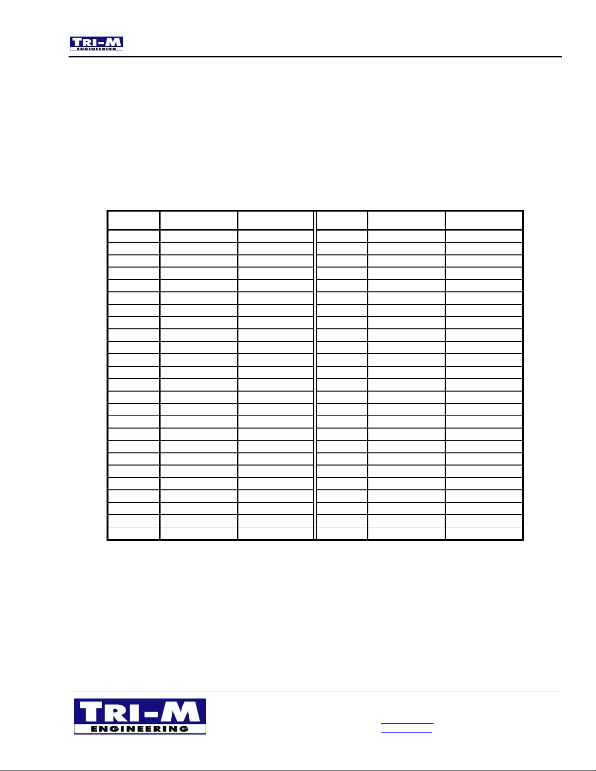
4.11 Compact Flash Connector (CN18)
Table 28: Compact Flash Connector (CN18)
Pin Signal Pin Type Pin Signal Pin Type
1
3
5
7
9
11
13
15
17
19
21
23
25
27
29
31
33
35
37
39
41
43
45
47
49
GND N/A
D04 I/O
D06 I/O
-CS0 Input
-ATA SEL Input
A08 Input
Vcc N/A
A05 Input
A03 Input
A01 Input
D00 I/O
D02 I/O
-CD2 Output
D11 I/O
D13 I/O
D15 I/O
-VS1 N/A
-IOWR Input
INTRQ Output
-CSEL Input
-RESET Input
-INPACK Output
-DASP I/O
D08 I/O
D10 I/O
2
4
6
8
10
12
14
16
18
20
22
24
26
28
30
32
34
36
38
40
42
44
46
48
50
D03 I/O
D05 I/O
D07 I/O
A10 Input
A09 Input
A07 Input
A06 Input
A04 Input
A02 Input
A00 Input
D01 I/O
-IOCS16 Output
-CD1 Output
D12 I/O
D14 I/O
-CS1 Input
-IORD Input
-WE Input
Vcc N/A
-VS2 N/A
IORDY Output
-REG Input
-PDIAG I/O
D09 I/O
GND N/A
Tri-M Engineering Tel: 800.665.5600, 604.945.9565
1407 Kebet Way, Unit 100 Fax: 604.945.9566
Port Coquitlam, BC V3C 6L3 E-mail: [email protected]
Canada Web site: www.tri-m.com
25
Page 28
24/04/2003 MZ-6SER Manual
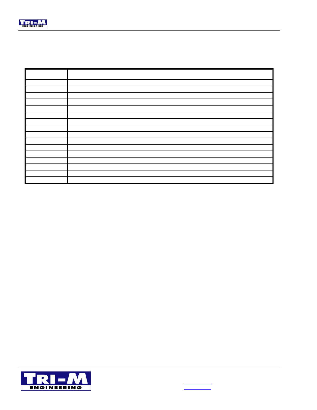
4.12 Interrupt and I/O Port assignments
Table 29: IRQ Interrupt
IRQ Number MZ-6SER Assignment
0 Systems timer (not available for other devices)
1 Keyboard controller (not available for other devices)
2 Second PIC cascade (not available for other devices)
3 Serial port two (COM2:)
4 Serial port one (COM1:)
5 Serial port three
6 Floppy disk controller (not available for other devices)
7 Parallel (printer) port one (LPT1:)
8 Real-time clock (RTC)
9 Unassigned
10 Serial port four
11 USB / Serial port five
12 PS/2 Mouse
13 Math coprocessor
14 Primary IDE
15 Secondary IDE / Serial port six
Tri-M Engineering Tel: 800.665.5600, 604.945.9565
1407 Kebet Way, Unit 100 Fax: 604.945.9566
Port Coquitlam, BC V3C 6L3 E-mail: [email protected]
Canada Web site: www.tri-m.com
26
Page 29
24/04/2003 MZ-6SER Manual
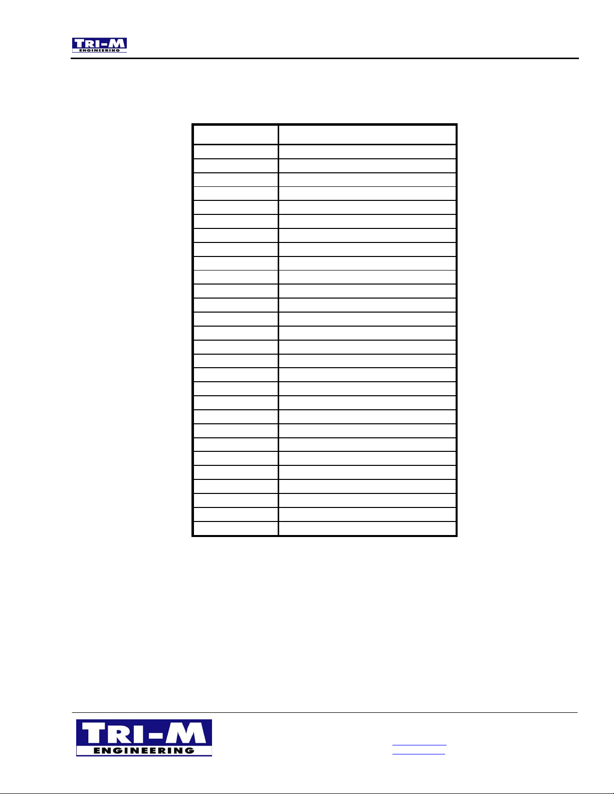
Table 30: I/O Port
I/O Address Hardware
0000 - 000F
0020 - 0021
0022 - 0021
0040 - 0043
0060 - 0060
0061 - 0061
0064 - 0064
0070 - 0071
0081 - 008F
0092 - 0092
00A0 - 00A1
00C0 - 00DF
00F0 - 00FF
02E0 – 02E7
02E8 – 02EF
02F0 – 02F7
02F8 - 02FF
0378 - 037F
03E8 – 03EF
03F0 - 03F5
03F7 - 03F7
03F8 - 03FF
0480 - 048F
04D0 - 04D1
0778 - 077F
0CF8 - 0CFF
AC00 - AC1F
AC80 - AC9F
DMA Controller
PIC
Motherboard Resources
System Timer
Keyboard
Systems Speaker
Keyboard
System CMOS / Real time clock
DMA Controller
Motherboard Resources
PIC
DMA Controller
Numeric Data Processor
Serial Port 5
Serial Port 4
Serial Port 6
Serial Port 2
Printer Port
Serial Port 3
Floppy Disk Controller
Floppy Disk Controller
Serial Port 1
Motherboard Resources
Motherboard Resources
Printer Port
PCI Bus
Motherboard Resources
Motherboard Resources
Tri-M Engineering Tel: 800.665.5600, 604.945.9565
1407 Kebet Way, Unit 100 Fax: 604.945.9566
Port Coquitlam, BC V3C 6L3 E-mail: [email protected]
Canada Web site: www.tri-m.com
27
Page 30

24/04/2003 MZ-6SER Manual
CHAPTER 5: BIOS SETTINGS
5.1 BIOS Setup
The MZ-6SER system BIOS (Basic Input Output System) supports a standard SETUP function
to configure system parameters. The BIOS uses these parameters to establish default
conditions during system initialization, both during the Power On Self Test (POST) phase, and
during system boot.
Using SETUP
To enter the SETUP function, press the <F2> key during POST.
Note: When you change SETUP parameters, the new values do not take effect until
the system is rebooted.
For details about how to set the various parameters using SETUP, please refer to the MachZ
BIOS Users Manual Supplement and the Phoenix BIOS 4.0 Rev 6 manual.
Customizing BIOS CMOS default
The CMOS default settings of the MZ-6SER can be customized by using the ZEB and
AMDFLASH utilities from ZFMicro. www.zflinux.com
The ZEB utility allows the majority of the CMOS parameters to be set to a particular value
which become the default settings when the MZ-6SER is powered up. ZEB modifies a BIOS
image file which is then programmed into the flash device using AMDFLASH utility. Please
note that setting the CMOS defaults is different from changing the CMOS settings. The CMOS
default settings only become effective when there is a no backup battery provided or when the
CMOS settings are cleared.
Tri-M Engineering Tel: 800.665.5600, 604.945.9565
1407 Kebet Way, Unit 100 Fax: 604.945.9566
Port Coquitlam, BC V3C 6L3 E-mail: [email protected]
Canada Web site: www.tri-m.com
28
Page 31
24/04/2003 MZ-6SER Manual
APPENDIX 1: OPTIONAL MZ104+UTIL UTILITY BOARD
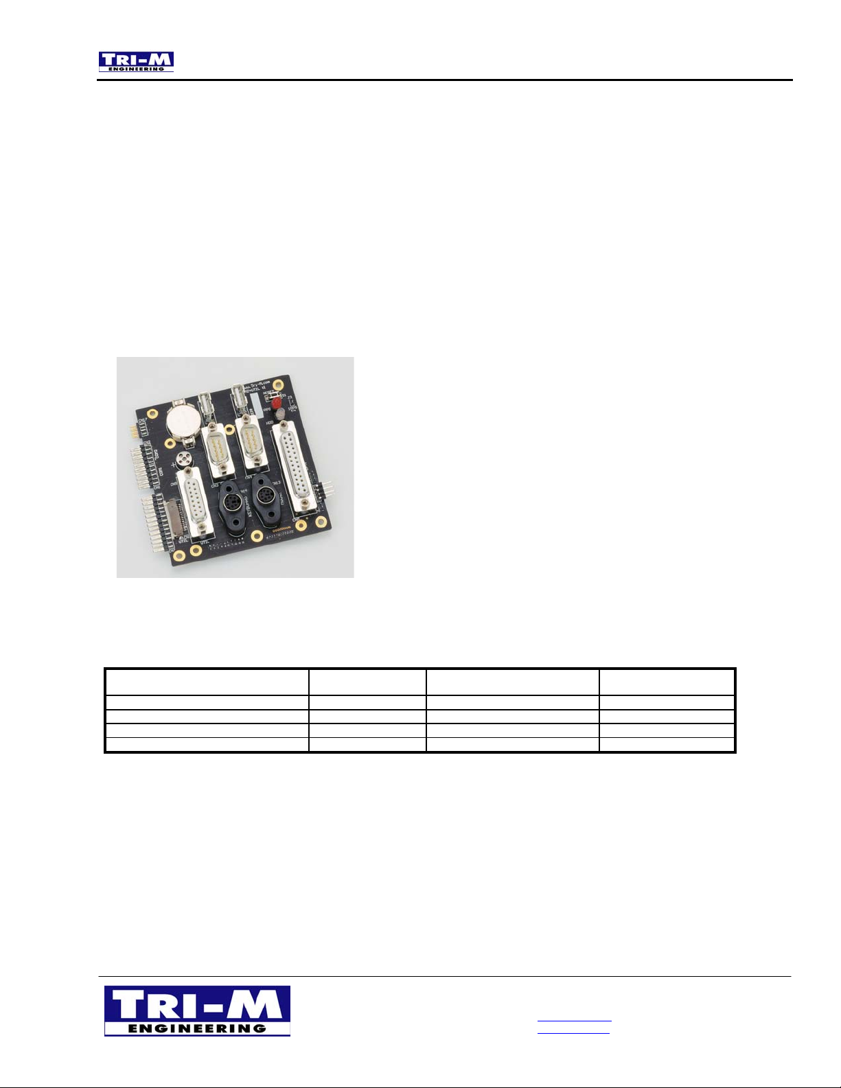
The MZ104+UTIL Utility Board, (see Figure 3) provides a convenient means to connect
peripheral devices to the MZ-6SER embedded CPU module. In addition, the MZ104+UTIL
provides input/output functionality of a status LED, and a hardware-reset switch. For
applications requiring a GPS receiver, the Utility Board also acts as carrier board to mate with
several models of Royaltek GPS receivers available from Tri-M Systems.
The MZ104+UTIL interfaces to the MZ-6SER CPU module via three ribbon cables and one
flex-foil cable. The MZ104+UTIL can be mounted above the MZ-6SER with PC/104 stand offs.
Figure 3: MZ104+UTIL Utility Connector Board
Table 31: MZ104+UTIL104 Interface
Cable Function MZ-6SER Utility Board
8-pin (2x4) IDC ribbon cable USB CN11 CN17
20-pin (2x10) IDC ribbon cable COM1/COM2 CN1/CN2 CN1/CN2
26-pin (2x13) IDC ribbon cable Parallel CN13 CN7
16-pin flex-foil cable Utility CN8 CN12
The MZ104+UTIL supports the Royaltek REB2000/2100 series as well as the REB12R series
GPS receivers. A 10-position single-row female socket is provided for REB2000 series
receiver while a 20-position dual-row female socket is provided for REB12R series receiver.
Power is provided to the MZ104+UTIL board through connector CN7 on the MZ-6SER. No
separate power source is required.
Tri-M Engineering Tel: 800.665.5600, 604.945.9565
1407 Kebet Way, Unit 100 Fax: 604.945.9566
Port Coquitlam, BC V3C 6L3 E-mail: [email protected]
Canada Web site: www.tri-m.com
29
Page 32

24/04/2003 MZ-6SER Manual
APPENDIX 2: LITERATURE REFERENCES
The following references are for information about the PC/104 architecture, the PC DOS, and
the PC BIOS.
ISA System Architecture
MindShare, Inc., Tom Shanley and Don
Anderson
Internet: [email protected]
CompuServe: 72507,1054
Published by Addison Wesley, Inc.
AT Bus Design
Edward Solari
Anabooks
12145 Alta Carmel Ct., Suite 250
San Diego, CA 92128
ISBN 0-929392-08-6
Personal Computer Bus Standard P996
Institute of Electrical and Electronic
Engineers, Inc.
445 Hoes Lane
Piscataway, NJ 08854
DiskOnChip
M-Systems Corp
8371 Central Avenue Suite A
Newark, CA 94560
Phone: 510-494-2090
FAX: 510-494-5545
MachZ
ZF Linux Devices, Inc.
1052 Elwell Court
Palo Alto, CA 94301
Phone: 650-940-4793
FAX: 650-965-4050
PC Interrupts
PC Interrupts, Ralf Brown,
Addison/Wesley.
BIOS Reference
System BIOS for IBM PC/XT/AT
Computers, Phoenix, Addison/Wesley
PC/104 Consortium
809 B-175 Cuesta Drive,
Mountain View, CA 94040
Phone: 415 903-8304
FAX: 415 967-0995
Tri-M Engineering Tel: 800.665.5600, 604.945.9565
1407 Kebet Way, Unit 100 Fax: 604.945.9566
Port Coquitlam, BC V3C 6L3 E-mail: [email protected]
Canada Web site: www.tri-m.com
30
 Loading...