


TriGem MVP3 Micro-ATX Motherboard (Delhi-III)
Table of Contents
I. Introduction
1. Generation Description ------------------------------------------------------------ 2
2. Function Block Diagram ------------------------------------------------------------ 4
II. System Overview
1. Major Units ------------------------------------------------------------------------ 5
2. Upgradeability -------------------------------------------------------------------- 6
2-1. Processor -------------------------------------------------------------------- 6
2-2. Memory --------------------------------------------------------------------- 6
2-3. BIOS ------------------------------------------------------------------------- 7
2-4. Expansion Slot ------------------------------------------------------------ 7
2-5. Advanced Configuration and Power Interface (ACPI) ----------------- 8
2-5. Manufacturing Options ------------------------------------------------------- 8
III. Jumper & Connector Description
1. Motherboard Jumper Setting------------------------------------------------------- 9
1-1. DIP Switch Setting Method ----------------------------------------------- 9
1-2. Jumper Setting Method --------------------------------------------------- 10
2. Motherboard Connector Description ------------------------------------------- 12
2-1. Motherboard Internal Connector --------------------------------------- 12
2-2. Motherboard External I/O Port ------------------------------------------- 15
1 / 15

3. Joystick & USB daughter board ------------------------------------------------ 15
2 / 15

I. Introduction
The Delhi-III Micro ATX motherboard offers a time to market consumer and corporate desktop solution featuring
the Pentium(R) processor with 60/66/75/83/95/100MHz front side bus and the MVP3 AGPsets in a Micro ATX low
profile motherboards. In addition, the integrated graphics components have been upgraded with the AGP graphics
controller and 4 or 8MB of SDRAM.
The Delhi-III motherboard was designed to be highly-minimized system cost . In this effort a smaller form factor,
Micro-ATX, gives the greater space economy and more affordable systems. Integrating AGP graphics controller
and SDRAM, as well as ISA audio solution onto the motherboard eliminates the need for more expensive graphic
and audio add-in cards. The end result is a system platform with a primary component level of integration with
translates into affordable solution for entry level users.
1. General description
Motherboard
Small PCB size in the Micro ATX form factor (ATX V1.2 form factor)
227mm * 244mm * 1.6t (4 Layers)
Processor
Socket 7 (321pin ZIF Socket)
Intel / AMD / Cyrix / IDT / IBM Pentium compatible processor support
- Intel P54C (75/90/100/133/166/200) and P55C with MMX (166/200/233)
- AMD K5 (75/90/100/120/133), K6 (166/200/233/266/300), and K6-2(3D) (233/266/300/333/350)
- Cyrix 6x86 (120/133/150/166), 6x86MX (166/200/233/266), and M-II(300/333/350)
- IDT C6 (180/200/225/240/266/300/333)
Main Chipset
AGPsets PCI/AGP Controller : VIA Apollo MVP3 VT82C598MVP
PCI bus mastering controller, and Power management interface : VIA VT82C596 or VT82C596A
Graphics : ATi RAGE-3D IIc with 4 or 8MB SDRAM
Audio : Crystal CS4235
Super I/O : Winbond W83877TF
DC-DC Converter : SC1152
Clock : IMI SG745BYB (60/66/75/83/90/100MHz host clock support)
3 / 15

Memory Configuration
System Memory
- Two banks of 3.3V EDO/SDRAM (168pin unbuffered DIMM) with max 256MB
- EDO/SDRAM operation in 66MHz front side bus and 100MHz SDRAM with 100MHz FSB.
Flash Memory : Programmable 2MB Flash memory
I/O Feature
Integrated standard I/O functions in the rear side
- One multi-mode parallel port
- One FIFO serial ports and optional port by header type
- PS/2 style keyboard and mouse port
- One USB port
- Three audio jack for Line input, Speaker output and MIC input
Integrated standard I/O functions in the front side
- One Joystick port
- One USB port
4 / 15

Audio Subsystem
Crystal CS4235 audio controller with fully plug and play ISA compatible function
Compatible with sound blaster, sound blaster pro, and window sound system
Enhanced Stereo full duplex operation
Advanced MPC3-compatible input and output mixer
Joystick port and MPU-401 compatible MIDI interface
Graphics Subsystem
General features
- Fully PC98 compliant
- Triple 8-bit palette DAC with gamma correction for true WYSIWYG color
- DDC1 and DDC2B+ for plug and play monitors
- Flexible graphics memory configuration : 4MB or 8MB SDRAM
2D Acceleration
- Hardware acceleration of Bitblt, Line Draw, Polygon / Rectangle Fill Masking, Monochrome
Expansion, Panning/Scrolling, Scissoring, full ROP support and hardware cursor
- Acceleration in 8/16/24/32bpp modes.
- Increased display FIFO from 24 to 32 DWORDS
3D Acceleration
- Hidden surface removal using 16-bit z-buffering
- Full support for Direct3D texture lighting
- Dithering support in 16bpp for near 24bpp quality in less memory
5 / 15

2. Function Block Diagram
Pentium Processor
SDRAM
HD
HA GMD GMA
North bridge GAD
MD
RGB Video
MA
Memory
[Rear side port]
AD PCI slots
CDROM HDD
HD Data
HD Addr South bridge
XD SD
ISA slots
BIOS SA
Speaker
6 / 15
ATi
L2 cache
8679F
FDD MIC
Line_in
Keyboard
Mouse
W83877TF Joystick
Serial
Parallel
USB
USB
[Front Side]
[Rear side Port]
II. System Overview
1. Major Units
Sound Chip
(CS4235)
AGP Graphics
7 / 15
I/O
8679F
Cryst
al
8679F

(ATi Rage-IIC)
SDRAM (4MB) L2 Cache (PBSRAM)
SDRAM (4MB, Upgrade) North Bridge
(MVP3)
Clock (SG745BYB)
South Bridge
(VT82C596 or VT596A) Socket-7
Tag RAM
Super I/O
(W83877TF)
Battery (3V)
Flash ROM (2MB)
8 / 15

2. Upgradeability
2-1. Processor
Delhi-III motherboard provides the 321pin ZIF socket-7 that is backward compatible with ZIF socket-5
processors. The Pentium processor have the variable CoreVCC voltage according to the model and vendor, so
the voltage regulator should be designed in the motherboard. SC1152 switching regulator offers the higher
efficiency and programmability of output voltage from 2.0V to 3.5V in 100mV increments with the VID pins.
Voltage selection
SC1152 DC-DC converter operates at a fixed frequency of 100KHz, providing an optimum compromise
between size, efficiency and cost in the intended application areas. The output voltage can be adjusted in
100mV increment or decrement according to the VID pin status.
Output voltage = minimum 2.0V, 2.1V, 2.2V, .... 3.2V, 3.3V, 3.4V, maximum 3.5V
Especially the old Pentium processors have to operate in the single power source, so must be carefully
adjusted or set within the recommended specification.
Supported Pentium processor group
Intel : P54C and P55C with MMX
AMD : K5, K6, and K6-2 with 3D Technology
IBM/Cyrix : 6x86, 6x86MX, and M-II
IDT : WinChip C6 Processor
2-2. Memory
The motherboard has two, dual inline memory module (DIMM), minimum 16MB to maximum 256MB memory
size. The BIOS can automatically detect the memory type, size, and speed through SMBUS interface between
the core chipset and DIMM module.
9 / 15

The motherboard supports the following memory features
3.3V and unbuffered168-pin DIMM
Voltage detection
3.3V Version 5V Version
Unbuffered detection
Unbuffered Buffered
66MHz and 100MHz unbuffered SDRAM, and also EDO DRAM
Non-ECC memory and ECC memory support
Single or double-sided DIMM with the following types
DIMM size Non-ECC memory ECC memory
16MB 2Mbit * 64bit 2Mbit * 72bit
32MB 4Mbit * 64bit 4Mbit * 72bit
64MB 8Mbit * 64bit 8Mbit * 72bit
128MB 16Mbit * 64bit 16Mbit * 72bit
10 / 15
2-3 BIOS
The motherboard uses a TriGem-AMI BIOS, which is stored in flash memory and can be upgraded using a disk-
based program. A new version of the BIOS can be upgraded from a diskette using the Flash Memory Update
utility.
Flash memory organization
Address (Hex) Size Functional description
FFFF0000 - FFFFFFFF 64KB Boot block
FFFA0000 - FFFEFFFF 256KB Main BIOS block
FF9F0000 - FFF9FFFF 8KB Used by BIOS (Event logging)
FFF9E000 - FFF9EFFF 8KB OEM logo or can flash area
FFF9C000 - FFF9DFFF 16KB DMI configuration data, PnP,
FFF90000 - FFF9BFFF 96KB Fault tolerant storage
FFF80000 - FFF8FFFF 64KB Fault tolerant backup block
On-board device management
The BIOS can manage the devices on the motherboard over the CMOS setup menu. However the built-in AGP
graphics controller can be disabled by the corresponding jumper as described Jumper Setting section later.
Device Description CMOS setup menu Default value
Internal Cache Pentium Processor Enable / Disable Enabled
External Cache 64K*64 PBSRAM Enable / Disable Enabled
PS/2 Mouse South Bridge (VT82C596x) Enable / Disable Enabled
USB Function South Bridge (VT82C596x) Enable / Disable Enabled
On board Sound CS4235 Enable / Disable Enabled
On board FDC Super I/O (W83877TF) Auto / Enable / Disable Auto
On board serial Super I/O (W83877TF) Auto / 3F8 / 2F8 / 3E8 / 2E8 Auto
On board parallel Super I/O (W83877TF) Auto / Disable / 378 / 278 / 3BC Auto
On board IDE South Bridge (VT82C596x) Disable / Primary / Secondary / Both Both
11 / 15

2-4. Expansion Slot
The motherboard support ISA, PCI and AGP function. ISA and PCI functions are extended to the additional slot
with two ISA and two PCI, and AGP function is designed in the motherboard with AGP graphics controller.
PCI configuration space map
Bus number Device number Function number Device
00 00 00 VIA VT82C598MVP (North bridge)
00 01 00 VIA VT82C596x (South bridge)
00 07 00 PCI/ISA bridge (South bridge)
00 07 01 IDE bus master (South bridge)
00 07 02 USB (South bridge)
00 07 03 Power management (South bridge)
01 00 00 ATi Rage IIC graphics controller (AGP)
00 13 00 PCI slot1
00 12 00 PCI slot2
PCI interrupt & master number routing map
The VT82C596 PCI/ISA bridge has four programmable interrupt request input signals. Any PCI interrupt source
connects to one of these interrupts signals and assigned to the free proper interrupt number by PnP BIOS.
SB INT
signals
First
PCI slot
Second
PCI slot
AGP *
graphics
PIIX4e
USB device
PIRQA INTA INTB INTA
PIRQB INTB INTC
PIRQC INTC INTD
PIRQD INTD INTA INTA
Master REQ0 REQ1
IDSEL AD30 AD29 AD18
12 / 15

Note
Also AGP graphics controller does not use any PCI interrupt in the Delhi-III motherboard, because the
interrupt function of AGP graphics controller was designed to disabled status. For more information, please
contact the technical support team.
2-5. Advanced Configuration and Power Interface (ACPI)
The motherboard and system BIOS support the ACPI that requires an ACPI-aware operating system such as
Windows-NT 5.0 or Windows 98. ACPI feature include
Plug and play and APM functionality normally contained in the BIOS
Power management control of individual devices : add-in cards, hard disk drives, USB devices, and Video
A soft-off feature that enables operating system to power off the computer
Support for multiple wakeup events
Indication LED for normal mode (Amber), standby mode (Blinking Amber ), and suspend mode (Green)
but this function is dependent on the LED logic.
Wakeup devices and events
Wakeup device Wakeup events and functionality
Power switch Wakeup from Power-off status and power-off function
LAN Wakeup from power-off status
Modem Wakeup from power-off status
Thermal event Wakeup from power-off status
Sleep button Wakeup from power-off status and go to suspend mode (option)
2-6. Manufacturing Options
The motherboard has several manufacturing option according to OEM/ODM requirement. Make sure that these
options can be applied in the assembly stage, and it’s impossible to upgrade or change in the customer field.
Option items Selectable functionality Feature changes
Joystick port Front side / Rear side Use additional board or not
13 / 15

USB port Front side / Rear side Use additional board or not
LM78 Installation / No device built-in H/W sensor on LDCM
Graphics controller Rage-IIc / Rage pro AGP mode (1x or 2x)
Graphics memory 4MB / 8MB Two / four SDRAM configuration
14 / 15
III. Jumper & Connector Description
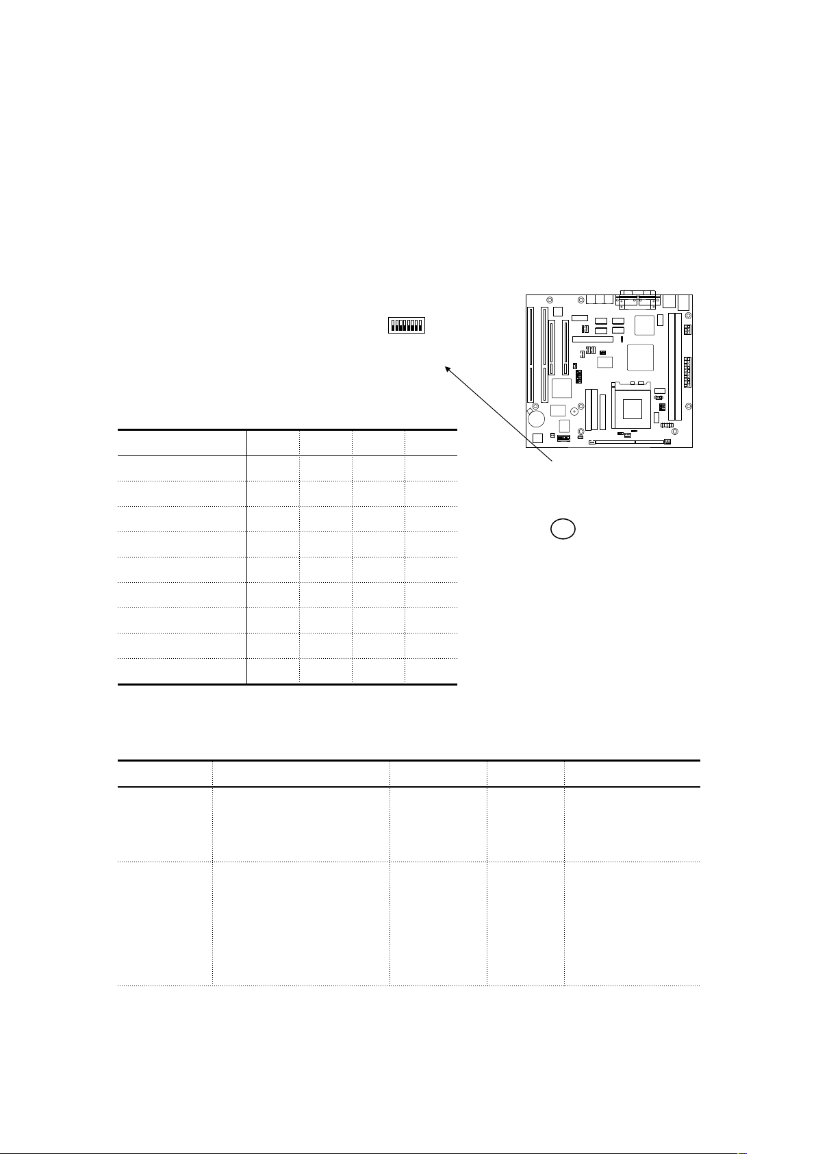
1. Motherboard Jumper Setting
1-1. DIP Switch Setting Method
CPU CoreVCC set
CoreVCC SW1 SW2 SW3 SW4
2.2V OFF ON OFF OFF
2.5V ON OFF ON OFF
2.7V ON ON ON OFF
2.8V OFF OFF OFF ON
2.9V ON OFF OFF ON
3.2V OFF OFF ON ON
3.3V ON OFF ON ON
3.4V OFF ON ON ON
3.5V ON ON ON ON
To set the CoreVCC correctly, please refer the CPU specification sheet and set J15 together.
CPU Vendor CPU Model CoreVCC IOVCC Remarks
Intel P54C/P54CS
P55C-MMX
3.5V (VRE)
3.4V (STD)
2.8V
IOVCC
IOVCC
3.3V
IOVCC = CoreVCC
IOVCC = CoreVCC
AMD K5
K6-PR233 (0.35um)
K6-166/200 (0.35um)
K6-233/266/300 (0.25um)
3.5V (VRE)
3.4V (STD)
3.2V
2.9V
2.2V
IOVCC
IOVCC
3.3V
3.3V
3.3V
IOVCC = CoreVCC
IOVCC = CoreVCC
15 / 15
OFF
ON
8 7 6 5 4 3 2 1

K6-2-300/333/350 (0.25um) 2.2V 3.3V
IBM/Cyrix 6x86
6x86MX
M-II
3.5V (VRE)
2.9V
2.9V
IOVCC
3.3V
3.3V
IOVCC = CoreVCC
IDT WinChip C6 (0.35um)
WinChip 2-3D (0.25um)
3.5V
3.3V
2.8V
IOVCC
IOVCC
3.3V
IOVCC = CoreVCC
IOVCC = CoreVCC
Other functionality
DIP Switch Function ON OFF
SW5 CMOS RAM function Clear CMOS RAM Enable write/save
SW6 Password function Clear password Enable password
SW7 CMOS setup function Disable to edit CMOS contents Enable to edit CMOS contents
SW8 FDD write protect Disable to write data
to Floppy disk
Enable to write data
to Floppy disk
16 / 15

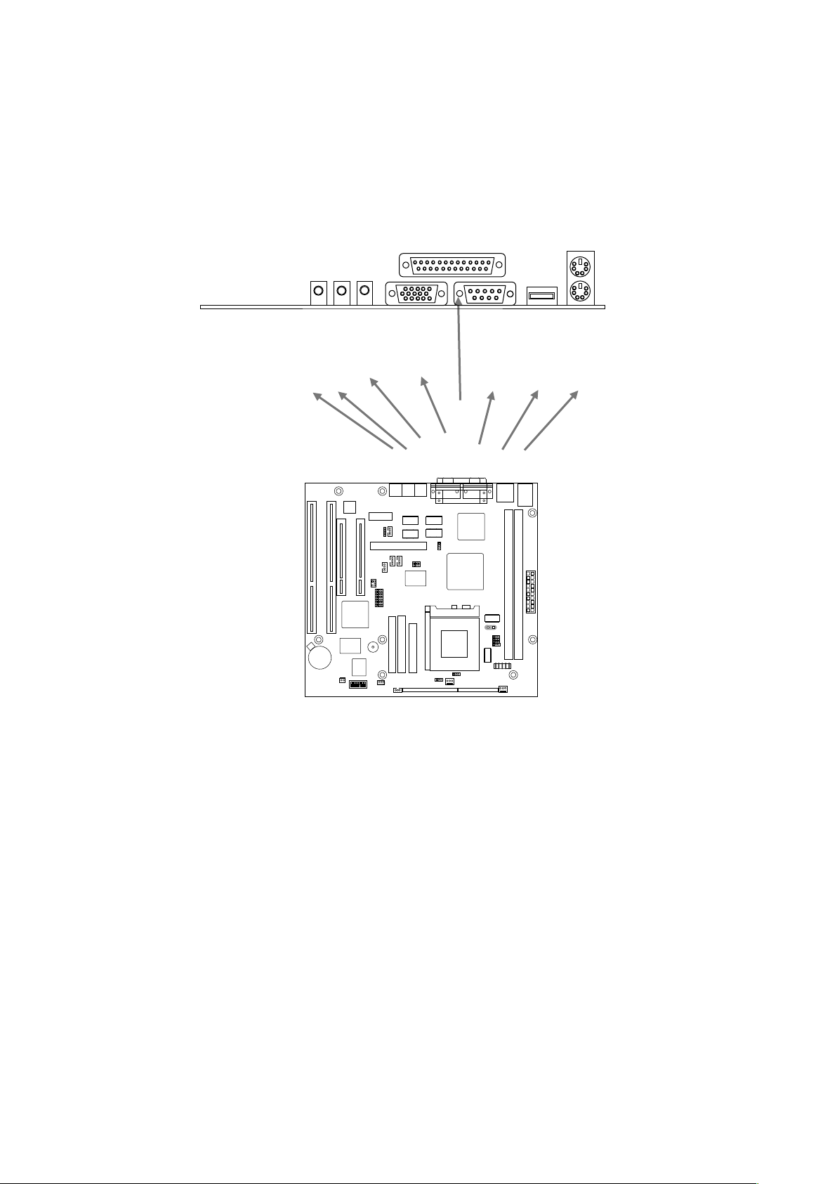
1-2. Jumper Setting Method
IOVCC set
This jumper is used for set of the CPU voltage like as the CoreVCC set. Mostly the Pentium processor uses two
kind of power source - CoreVCC and IOVCC, and the corresponding voltage level should be adjusted as
recommended in the CPU specification.
J15 CPU Type
1-2 IOVCC = CoreVCC ( single CPU power source )
2-3 (default) IOVCC = 3.3V ( dual CPU power source )
AGP graphics device function
This jumper does set the functionality of the built-in AGP graphics controller
J10 AGP device functionality
1-2 Disable AGP graphics controller built in the motherboard
2-3 (default) Enable AGP graphics controller built in the motherboard
17 / 15
1 2 3
J15
1 2 3
J2
J9
J3
J4
J5
J7
J8
1 2 3
J11
J12
J13
J14
J10
1
2
3
1 2 3
J16
J17

L2 cache functionality
This jumper does set the functionality of L2 cache
J14 L2 cache functionality
1-2 (default) Interleave mode
2-3 Linear mode
OEM/ODM selector
These jumpers (J7 & J8) will be optional parts for the OEM/ODM logo message selector.
Memory Clock Selector
These jumpers can set the frequency of the DIMM memory (66, 75, 83, 90, and 100MHz )
For the proper operation, these jumpers should be set together.
J16 J17 DIMM Module Frequency Selector Memory Type
2-3 1-2 66MHz Only 66MHz & 100MHz SDRAM, EDO
1-2 2-3 Depend on CPU clock (66/75/83/90/100MHz) 100MHz SDRAM only
18 / 15

CPU frequency set
To set the CPU frequency correctly, the proper combination should be selected in the CPU vendor, type, and
the internal speed.
BF0/BF1/BF2 : Set the bus speed ratio of CPU =================> (J11,J12,J13)
FS0/FS1/FS2 : Set the host clock frequency of the clock generator => (J3,J4,J5)
HA26/HA27 : Set the ratio between PCI clock and the host clock => (J2,J9)
BF0/BF1/BF2 functionality are different with the CPU vendor.
CPU Vendor & Type Freq. Bus Ratio J3 J4 J5 J2 J9 J11 J12 J13
Intel P54C 90MHz 90 60 1.5x 2-3 2-3 2-3 2-3 2-3 1-2 1-2 1-2
Intel P54C 100MHz 100 66 1.5x 1-2 2-3 2-3 2-3 2-3 1-2 1-2 1-2
Intel P54C 120MHz 120 60 2.0x 2-3 2-3 2-3 2-3 2-3 2-3 1-2 1-2
Intel P54C 133MHz 133 66 2.0x 1-2 2-3 2-3 2-3 2-3 2-3 1-2 1-2
Intel P54C 150MHz 150 60 2.5x 2-3 2-3 2-3 2-3 2-3 2-3 2-3 1-2
Intel P54C 166MHz 166 66 2.5x 1-2 2-3 2-3 2-3 2-3 2-3 2-3 1-2
Intel P55C 166MHz 166 66 2.5x 1-2 2-3 2-3 2-3 2-3 2-3 2-3 1-2
Intel P55C 200MHz 200 66 3.0x 1-2 2-3 2-3 2-3 2-3 1-2 2-3 1-2
Intel P55C 233MHz 233 66 3.5x 1-2 2-3 2-3 2-3 2-3 1-2 1-2 1-2
AMD K5 PR90 90 60 1.5x 2-3 2-3 2-3 2-3 2-3 1-2 1-2 1-2
AMD K5 PR100 100 66 1.5x 1-2 2-3 2-3 2-3 2-3 1-2 1-2 1-2
AMD K5 PR120 90 60 1.5x 2-3 2-3 2-3 2-3 2-3 1-2 1-2 1-2
AMD K5 PR133 100 66 1.5x 1-2 2-3 2-3 2-3 2-3 1-2 1-2 1-2
AMD K6 PR166 166 66 2.5x 1-2 2-3 2-3 2-3 2-3 2-3 2-3 1-2
AMD K6 PR200 200 66 3.0x 1-2 2-3 2-3 2-3 2-3 1-2 2-3 1-2
AMD K6 PR233 233 66 3.5x 1-2 2-3 2-3 2-3 2-3 1-2 1-2 1-2
AMD K6 PR266 266 66 4.0x 1-2 2-3 2-3 2-3 2-3 2-3 1-2 2-3
AMD K6 PR300 300 66 4.5x 1-2 2-3 2-3 2-3 2-3 2-3 2-3 2-3
AMD K6-2 3D PR266 266 66 4.0x 1-2 2-3 2-3 2-3 2-3 2-3 1-2 2-3
AMD K6-2 300-66 300 66 4.5x 1-2 1-2 1-2 1-2 2-3 2-3 2-3 2-3
19 / 15

AMD K6-2 333-66 333 66 5.0x 1-2 1-2 1-2 1-2 2-3 1-2 2-3 2-3
AMD K6-2 3D PR300 300 100 3.0x 1-2 1-2 1-2 1-2 2-3 1-2 2-3 1-2
AMD K6-2 3D PR350 350 100 3.5x 1-2 1-2 1-2 1-2 2-3 1-2 1-2 1-2
IBM/Cyrix 6x86 PR150+ 120 60 2.0x 2-3 2-3 2-3 2-3 2-3 2-3 1-2 1-2
IBM/Cyrix 6x86 PR166+ 133 66 2.0x 1-2 2-3 2-3 2-3 2-3 2-3 1-2 1-2
IBM/Cyrix 6x86MX PR166 150 60 2.5x 2-3 2-3 2-3 2-3 2-3 2-3 2-3 1-2
IBM/Cyrix 6x86MX PR200 166 66 2.5x 1-2 2-3 2-3 2-3 2-3 2-3 2-3 1-2
IBM/Cyrix 6x86MX PR233 200 66 3.0x 1-2 2-3 2-3 2-3 2-3 1-2 2-3 1-2
IBM/Cyrix 6x86MX PR266 210 60 3.5x 2-3 2-3 2-3 2-3 2-3 1-2 1-2 1-2
IBM/Cyrix M-II PR300 233 66 3.5x 1-2 2-3 2-3 2-3 2-3 1-2 1-2 1-2
IBM/Cyrix M-II PR333 250 83 3.0x 1-2 2-3 1-2 1-2 1-2 1-2 2-3 1-2
IBM/Cyrix M-II PR350 270 90 3.0x 1-2 2-3 2-3 1-2 2-3 1-2 2-3 1-2
IBM/Cyrix M-II PR366 262 75 3.5x 2-3 2-3 1-2 1-2 1-2 1-2 1-2 1-2
IDT WinChip C6 180 180 60 3.0x 2-3 2-3 2-3 2-3 2-3 1-2 2-3 1-2
IDT WinChip C6 200 200 66 3.0x 1-2 2-3 2-3 2-3 2-3 1-2 2-3 1-2
IDT WinChip C6 225 225 75 3.0x 2-3 2-3 1-2 1-2 1-2 1-2 2-3 1-2
IDT WinChip C6 240 240 60 4.0x 2-3 2-3 2-3 2-3 2-3 2-3 1-2 2-3
IDT WinChip C6 266 266 66 4.0x 1-2 2-3 2-3 2-3 2-3 2-3 1-2 2-3
20 / 15

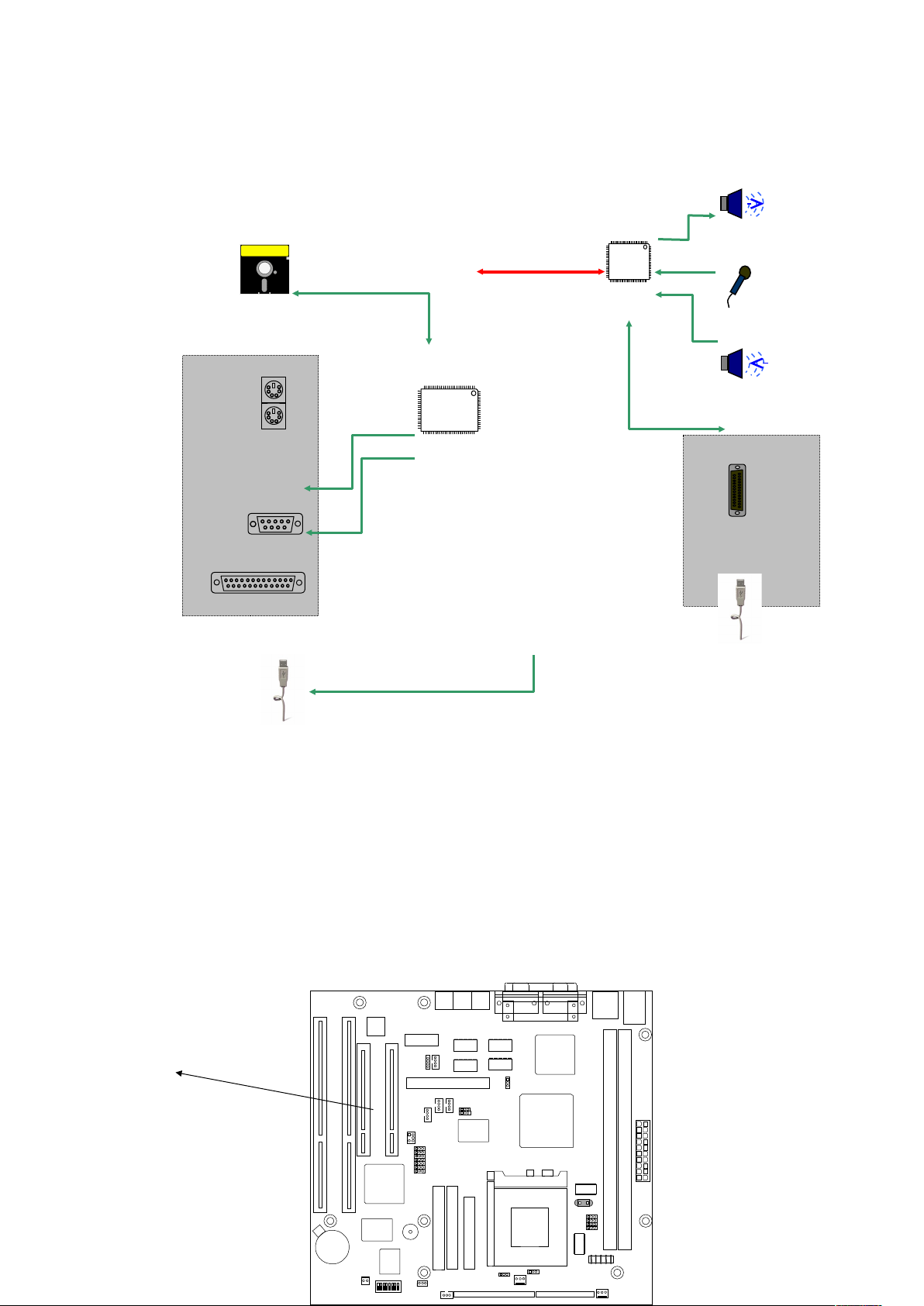
2. I/O Header Connector Description
2-1. Motherboard Internal Connector
Joystick & USB Header (CN1,CN40)
AMC connector (CN6)
ISA (CN18, CN17)
PCI (CN13, CN12)
Modem Sound (CN11, CN14)
CD Sound (CN9, CN15) DIMM Module
Video Sound (CN8) ATX PSU connector (CN7)
Pri-IDE connector (CN16)
PC/PCI (CN5) Sec-IDE connector (CN10)
FDD connector (CN21)
Chassis Intrusion (CN3)
LAN Wakeup (CN4) Chassis FAN (CN28)
Aux.-Indicator Header (CN23)
Indicator Header (CN20)
Modem Wakeup (CN19) CPU FAN (CN2)
CPU FAN (CN41)
21 / 15

CPU FAN connector (CN2,CN41)
Pin number Signal description
1 GND
2 FAN power
3 Tachometer (speed)
Pin number Signal description
1 GND
2 +12V
3 GND
Chassis FAN connector (CN28)
Pin number Signal description
1 GND
2 FAN control
3 Tachometer (Speed)
22 / 15
1 2 3
CN2
1 2 3
1 2 3
CN41

PC/PCI connector (CN5)
Pin Signal description Pin Signal description
1 /PCGNTA 4 /PCREQA
2 GND 5 N.C
3 Key 6 SER_IRQ
Joystick connector (CN1,CN40)
Pin Signal description Pin Signal description
1 VCC 9 VCC
2 GD(4) 10 GD(6)
3 GD(0) 11 GD(2)
4 GND 12 MIDI OUT
5 GND 13 GD(3)
6 GD(1) 14 GD(7)
7 GD(5) 15 MIDI IN
8 VCC 16 Key
1 GND 3 Positive DATA
2 Negative DATA 4 VCC
Video Sound (CN8)
Pin Signal description Pin Signal description
1 Left Sound 3 GND
2 GND 4 Right Sound
Modem Sound (CN11, CN14)
Pin Signal description Pin Signal description
1 MIC 4 GND
2 GND 5 MONO IN
23 / 15
2 4 6
1 3 5
1 2 3 4
1 2 3 4 5
CN14
3 1 8 7 6 5 4 3 2 1
4 2 16 15 14 13 12 11 10 9

3 MONO OUT
Pin Signal description Pin Signal description
1 MONO IN 3 GND
2 GND 4 MIC
CD Sound (CN9, CN15)
Pin Signal description Pin Signal description
1 Left Sound 3 GND
2 GND 4 Right Sound
Pin Signal description Pin Signal description
1 GND 3 GND
2 Left Sound 4 Right Sound
24 / 15
1 2 3 4
ATAPI CD (CN9)
1 2 3 4
CN11
1 2 3 4
Mitsumi CD (CN15)

LAN Wakeup (CN4)
Pin Signal description Pin Signal description
1 +5VSB 3 LANWK
2 GND
Modem Wakeup (CN19)
Pin Signal description Pin Signal description
1 Modem Ring 3 +5VSB
2 GND
Indicator Header (CN20)
Pin Signal description Pin Signal description
1 VCC 12 GND
2 PM indicator signal 13 IRTX
3 GND 14 VCC
4 Key 15 IRSEL
5 VCC 16 N.C
6 HDD access signal 17 GND
7 Key 18 Key
8 Power-ON switch signal 19 VCC
9 GND 20 GND
10 Key 21 N.C
11 IRRX 22 Speaker signal
25 / 15
1 2 3 4
1 2 3 4
1 2 3 5 6 8 9 11 12 13 14 15 16 17 19 2 0 21 22
PWR HDD DC SW IrDA Speaker
2-2. Motherboard External I/O Port
Parallel port Mouse
MIC L_IN SPK Video COM1 USB Keyboard
3. Joystick & USB daughter board
Joystick USB
26 / 15

20pin Flat Cable
4. LED & Power S/W board
Power LED
HDD Access LED
Power Switch
LED board to board connector
Power LED color : Green (normal working)
Blinking Green (power management mode)
HDD LED color : Green light on (HDD access)
Light off (no access to HDD device)
27 / 15
 Loading...