

Page 1

Title
Wing4TRAX modem hardware OEM user manual
Reference
DSE-WING4TRAX OEM-User Manual v1.4.docx
Author
Pascal DARAGON
Stream
TRAX-Net
Security
Level 1 – Restricted
Version/Revision
1.4
Edition Date
20/07/2016
Status
Final
Version/Revision
Details
Date
Editor
1.0
Initial version
28/04/2016
P. DARAGON
1.1
Minor corrections & add typical design
06/05/2016
P. DARAGON
1.2
Change VDD range & add conformity information
22/06/2016
P. DARAGON
1.3
Conformity declarations upgrades & add LBT + AFA
05/07/2016
P. DARAGON
1.4
Add integration guidelines & product testing
20/07/2016
P. DARAGON
DSE
Revision History
Page 2

TRAX-Net module
Doc Reference
DSE-WING4TRAX OEM-User Manual
Page
2 / 33
DSE
Version/Revision
1.4
Date
20/07/2016
User’s manual
Security
Level 1 – Restricted
INDEX
1 Introduction .............................................................................................................................................................................................. 4
1.1 References .................................................................................................................................................................................................................. 4
1.2 Terms and abbreviations ..................................................................................................................................................................................... 4
1.3 General presentation ............................................................................................................................................................................................. 5
1.4 TRAX-Net at a glance ............................................................................................................................................................................................ 6
1.5 Main features ........................................................................................................................................................................................................... 8
1.6 Pinout definition ..................................................................................................................................................................................................... 9
2 Functional interfaces ........................................................................................................................................................................... 10
2.1 Typical design ....................................................................................................................................................................................................... 10
2.2 Host CPU ................................................................................................................................................................................................................. 10
2.3 Antenna ................................................................................................................................................................................................................... 11
2.4 GPIOs ........................................................................................................................................................................................................................ 11
2.5 ADC ............................................................................................................................................................................................................................ 12
2.6 SPI .............................................................................................................................................................................................................................. 12
2.6 I2C ............................................................................................................................................................................................................................. 12
2.7 EXT_IRQ ................................................................................................................................................................................................................... 12
3 Hardware Interfaces ............................................................................................................................................................................ 13
3.1 Absolute Maximum Ratings ............................................................................................................................................................................. 13
3.2 DC characteristics ............................................................................................................................................................................................... 13
3.3 RF characteristics ................................................................................................................................................................................................ 14
3.4 Mechanical characteristics .............................................................................................................................................................................. 16
3.5 Footprint characteristics .................................................................................................................................................................................. 17
4 Declarations of conformity ............................................................................................................................................................... 18
4.1 R&TTE conformity for 433 MHz and 863 MHz bands ........................................................................................................................... 18
4.2 FCC conformity for 915 MHz band ............................................................................................................................................................... 18
4.3 CSA conformity for 915 MHz band ............................................................................................................................................................... 19
5 Integration Guidelines ........................................................................................................................................................................ 20
5.1 Design Checklist ................................................................................................................................................................................................... 20
5.1.1 Schematics ....................................................................................................................................................................................................... 20
5.1.2 Layout ................................................................................................................................................................................................................. 20
5.1.3 Antenna ............................................................................................................................................................................................................. 21
5.2 Layout Recommendations ................................................................................................................................................................................ 21
5.2.1 Guidelines per pin function ...................................................................................................................................................................... 21
5.2.2 RF antenna connection ............................................................................................................................................................................... 21
5.3 Antenna Characteristics ................................................................................................................................................................................... 27
5.3.1 Antenna termination ................................................................................................................................................................................... 28
5.3.2 Antenna radiation ......................................................................................................................................................................................... 29
TRAXENS SAS – Les Baronnies – Bâtiment C – 15 Rue Marc Donadille – 13453 Marseille – France
SIRET 750 626 871 00016 ⎜APE 3320C ⎜Bureau : +33 4 91 11 88 16 ⎥ e-mail : info@traxens.com
Page 3

TRAX-Net module
Doc Reference
DSE-WING4TRAX OEM-User Manual
Page
3 / 33
DSE
Version/Revision
1.4
Date
20/07/2016
User’s manual
Security
Level 1 – Restricted
6 Product Testing ..................................................................................................................................................................................... 30
6.1 TRAXENS manufacturing tests ...................................................................................................................................................................... 30
6.2 Tests policy for OEM manufacturer .............................................................................................................................................................. 31
6.2.1 “GO/no GO” tests ........................................................................................................................................................................................... 31
6.2.2 Functional RF tests ....................................................................................................................................................................................... 31
7 Disclaimers ............................................................................................................................................................................................. 33
7.1 Document Status .................................................................................................................................................................................................. 33
7.2 ESD ............................................................................................................................................................................................................................ 33
7.3 Warranty ................................................................................................................................................................................................................ 33
7.4 Disposal of waste by users in private households within the European Union ............................................................... 33
TRAXENS SAS – Les Baronnies – Bâtiment C – 15 Rue Marc Donadille – 13453 Marseille – France
SIRET 750 626 871 00016 ⎜APE 3320C ⎜Bureau : +33 4 91 11 88 16 ⎥ e-mail : info@traxens.com
Page 4

TRAX-Net module
Doc Reference
DSE-WING4TRAX OEM-User Manual
Page
4 / 33
DSE
Version/Revision
1.4
Date
20/07/2016
User’s manual
Security
Level 1 – Restricted
ID
Name
Author
Date
Version
R1
UART COMMUNICATION PROTOCOL WING4TRAX-HOST
N. GUZZO
16/06/2016
1.59
R2
DSE - W4T - HOSTCOM Test commands
P. DARAGON
05/07/2016
1.5
1 INTRODUCTION
This manual is intended solely to TRAXENS internal use, as part of the integration of Wing4TRAX module
into its asset tracking devices TRAX-Box and their derivatives, or to system integrators duly certified by
TRAXENS
All rights to this manual are the exclusive property of TRAXENS. All rights reserved. Copying this manual
without written permission from the owner via printing, copying, recording or by any other means, translating this manual in full or partially is prohibited.
1.1 REFERENCES
1.2 TERMS AND ABBREVIATIONS
AES Advanced Encryption Standard
AFA Adaptive Frequency Agility
AGFS Automatic Geographic-based Frequency Selection
CTS Clear To Send
FHSS Frequency Hopping Spread Spectrum
GMSK Gaussian Minimum Frequency Shift Keying
GPS Global Positioning System
GSM Global System for Mobile communications
ISM Industrial – Scientific – Medical
LBT Listen Before Talk
MAC Media Access Control (radio layer)
MCC Mobile Country Code
NET NETwork (radio layer)
NPM Network Phy Mode (message)
P2P Peer To Peer
PHY PHYsical (radio layer)
PIFA Planar Inverted-F Antenna
RTS Request To Send
UART Universal Asynchronous Receiver Transmitter
VSWR Voltage Standing Wave Ratio
WAN Wide Area Network
WOR Wake On Radio
WSN Wireless Sensor Network
TRAXENS SAS – Les Baronnies – Bâtiment C – 15 Rue Marc Donadille – 13453 Marseille – France
SIRET 750 626 871 00016 ⎜APE 3320C ⎜Bureau : +33 4 91 11 88 16 ⎥ e-mail : info@traxens.com
Page 5

TRAX-Net module
Doc Reference
DSE-WING4TRAX OEM-User Manual
Page
5 / 33
DSE
Version/Revision
1.4
Date
20/07/2016
User’s manual
Security
Level 1 – Restricted
1.3 GENERAL PRESENTATION
Wing4TRAX is a universal sub-GHz radio module with the native capability to support the 3 unlicensed ISM
bands available worldwide: 433 MHz, 868 MHz and 915 MHz
It has been designed to be connected to a host controller thru an UART interface, like a standard radio
modem. It embeds the robust and efficient TRAX-Net protocol stack, with P2P communication and/or
mesh routing capabilities, between single or several nodes registered into a TRAX-Net cluster
Selection of the working band depends on the country where the Wing4TRAX module is operated and is
performed thanks to a specific command issued by the host controller, using proprietary AGFS algorithm.
TRAXENS provides a fully portable ANSI-C library to be executed on the host controller, to select the proper
band as a function of geolocation information, gathered from multiple sources: GPS position, GSM MCC or
NPM messages broadcasted by other TRAX-Net nodes.
In any case, frequency hopping channels and RF output power are settled to be in conformity with local
regulations; if geolocation information is not available, Wing4TRAX module remains silent and enters by
default in sniffer mode, listening for a NPM message.
Note: AGFS algorithm controls the Wing4TRAX firmware execution and guarantees the non-infringement of
local radio regulations in force where the module is operated by a host controller; therefore, integrity and
conformity of AGFS algorithm implementation into the host controller is verified during the TRAXENS certification process of its own products, as for those developed by integrators
TRAXENS SAS – Les Baronnies – Bâtiment C – 15 Rue Marc Donadille – 13453 Marseille – France
SIRET 750 626 871 00016 ⎜APE 3320C ⎜Bureau : +33 4 91 11 88 16 ⎥ e-mail : info@traxens.com
Page 6
TRAX-Net module
Doc Reference
DSE-WING4TRAX OEM-User Manual
Page
6 / 33
DSE
Version/Revision
1.4
Date
20/07/2016
User’s manual
Security
Level 1 – Restricted
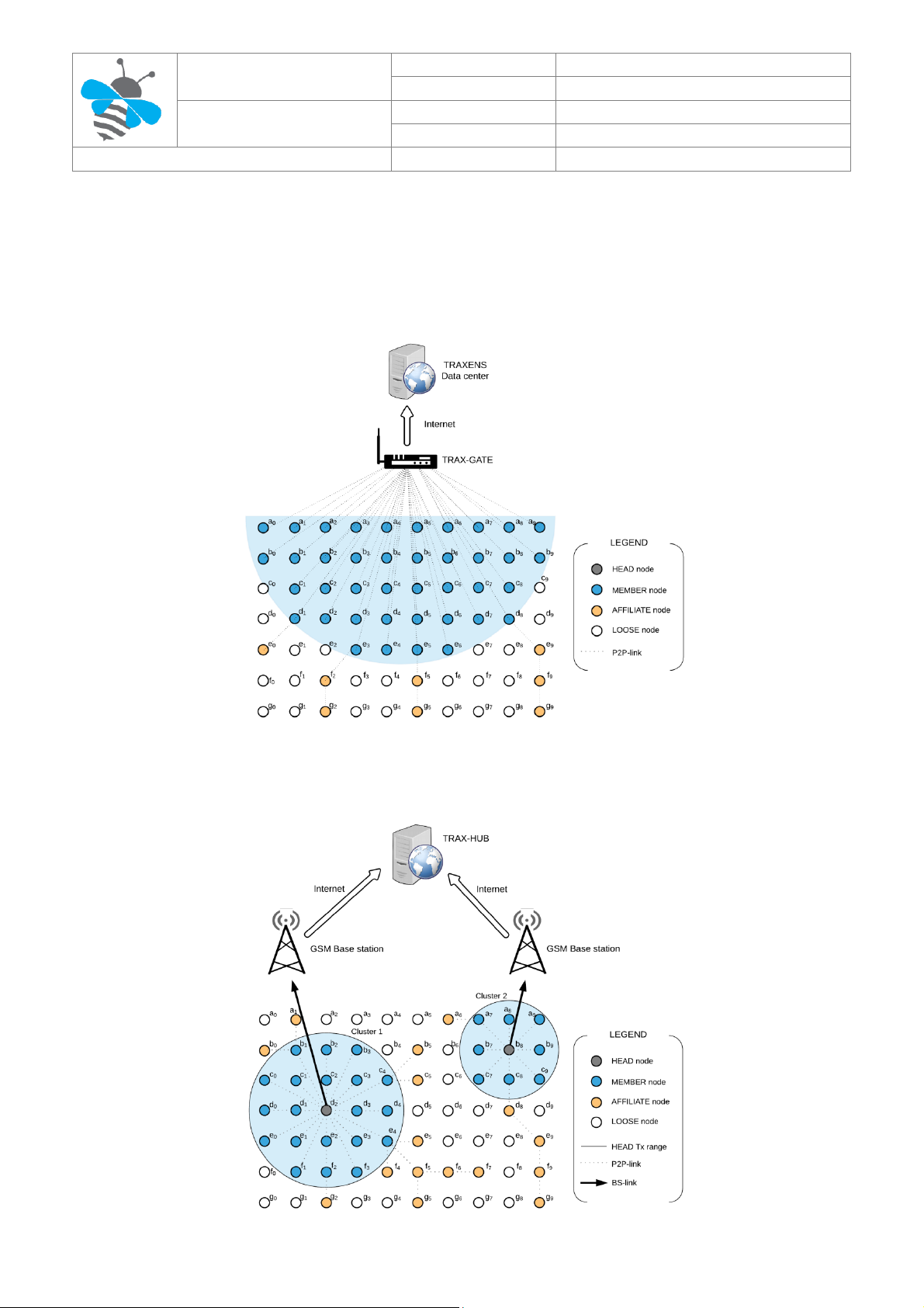
1.4 TRAX-NET AT A GLANCE
TRAX-Net is a cluster-based WSN protocol in which some nodes are in charge to aggregate the data
collected from other nodes and deliver it to the sink. The sink is either a TRAX-Gate gateway connected to a
WAN thru Ethernet, WiFi or GSM, or another TRAX-Net node with GSM connection capabilities
When a TRAX-Gate is present, it forms a super cluster and all TRAX-Net nodes in its communication range
join it, as illustrated below:
When no Gateway is present in the nearby, an election scheme selects some TRAX-Net nodes to be in
charge of collecting the data generated by the neighbors and transmit it to the TRAXENS data center passing through the GSM connection, as illustrated below:
TRAXENS SAS – Les Baronnies – Bâtiment C – 15 Rue Marc Donadille – 13453 Marseille – France
SIRET 750 626 871 00016 ⎜APE 3320C ⎜Bureau : +33 4 91 11 88 16 ⎥ e-mail : info@traxens.com
Page 7
TRAX-Net module
Doc Reference
DSE-WING4TRAX OEM-User Manual
Page
7 / 33
DSE
Version/Revision
1.4
Date
20/07/2016
User’s manual
Security
Level 1 – Restricted
Parameter
Value
Max number of members in a cluster
250
Max number of members in a super-cluster
Undefined
Max number of affiliates per member
16
Max hop-distance
8+1 hops
Max data in a packet
2500 Bytes
TRAX-Net protocol stack is divided into 3 main layers:
1. PHY, responsible for controlling the output power, channel frequency, modulation/demodulation,
symbol encoding/decoding and bit framing
2. MAC, responsible for controlling frame preamble, synchronization, packet format, node addressing
thanks to unique TRAX-Net ID, integrity checking and communication retries
3. NET, responsible for controlling cluster election policy, node status (HEAD, MEMBER, AFFILIATE,
LOOSE) and message routing thru the cluster
Each layer can be individually started by host controller, respecting a strict order: PHY layer first, followed
by MAC layer, then NET layer. Activation of PHY and MAC layers is direct thru specific commands; activation
of NET layer is conditioned to a prior mutual authentication between the host and Wing4TRAX module,
based on a shared secret AES key. This security has been put in place to avoid malicious generation of fake
TRAX-Net clusters, with intention to dump data of registered nodes and thus create a denial of service
Main features of TRAX-Net are listed in table below:
TRAXENS SAS – Les Baronnies – Bâtiment C – 15 Rue Marc Donadille – 13453 Marseille – France
SIRET 750 626 871 00016 ⎜APE 3320C ⎜Bureau : +33 4 91 11 88 16 ⎥ e-mail : info@traxens.com
Page 8

TRAX-Net module
Doc Reference
DSE-WING4TRAX OEM-User Manual
Page
8 / 33
DSE
Version/Revision
1.4
Date
20/07/2016
User’s manual
Security
Level 1 – Restricted
Technical specifications
Details
Module dimensions
35 x 17.5 x 2.9 mm
Operating temperature
-40°C to +85°C
Operating voltage (VDD)
1.8V to 3.6V (3.0V typical)
RF chip (8 bits µC + RF front end)
AX8052F143
PA voltage (VDD_ANA)
Regulated from VDD to 1.8V (1)
Tx consumption @433.92 MHz
51 mA typ. @+13dBm
Tx consumption @866.5 MHz
49 mA typ. @+13dBm
Tx consumption @921.5 MHz
47 mA typ. @+13dBm
Rx consumption
11 mA
WOR consumption
13.9 µA
Programmable TX power
From -10dBm to +13dBm
ETSI 433 MHz band channel mapping
17 channels of 100KHz
ETSI 868 MHz band channel mapping
68 channels of 100KHz
FCC 915 MHz band channel mapping
68 channels of 100KHz
ARIB 920 MHz band channel mapping
32 channels of 100KHz
Sensitivity @433.92 MHz
Down to -109dBm @BER 10-3
Sensitivity @866.5 MHz
Down to -113dBm @BER 10-3
Sensitivity @921.5 MHz
Down to -110dBm @BER 10-3
Operating range (open space)
Up to 1km with external antenna
Medium access method
ETSI compliant LBT + AFA
RF communication
Unicast, broadcast, mesh routing
RF data rate (raw bit / payload byte)
20Kbps / ~1.1Kbyte per second
Host communication
UART 19200, n, 8, 1
Digital inputs / outputs
Up to 12 (5V tolerant)
Analog inputs (10 bits ADC)
2 channels (0..1V) @20ksample/s
Smart kernel (PHY layer + bootloader)
MAC + NET layers upgradable thru UART
1.5 MAIN FEATURES
Wing4TRAX’s main features are listed in table below:
(1) Power amplifier (PA) runs from the regulated VDD_ANA supply and not directly from the battery voltage VDD. This has
the advantage that the current and output power do not vary much over supply voltage and temperature
TRAXENS SAS – Les Baronnies – Bâtiment C – 15 Rue Marc Donadille – 13453 Marseille – France
SIRET 750 626 871 00016 ⎜APE 3320C ⎜Bureau : +33 4 91 11 88 16 ⎥ e-mail : info@traxens.com
Page 9
TRAX-Net module
Doc Reference
DSE-WING4TRAX OEM-User Manual
Page
9 / 33
DSE
Version/Revision
1.4
Date
20/07/2016
User’s manual
Security
Level 1 – Restricted
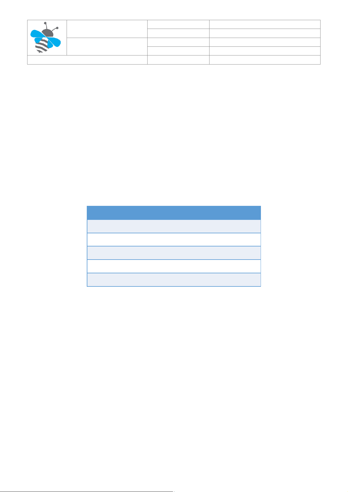
Pin
Type
RST value
Description
1 - VDD
Power supply
X
Source voltage between 2.3V & 3.6V – also pin 6
2 - PA2
Analog input
X
Channel 2 – 10bits ADC – [0..1V] range
3 - GND
Ground
X
Also pins 4, 7, 8, 9, 10, 11, 12, 13, 14, 15, 16, 18, 19, 20, 21, 22, 23, 24
5 - PA5
Analog input
X
Channel 5 – 10bits ADC – [0..1V] range
17 - ANT
Antenna RX-TX
X
Connect to a 50 antenna thru a 150pF coupling capacitor
25 - SYSCLK
Digital output
Hi-Z
Optional I2C clock line (SCL) or general purpose clock output
26 - PC4
Digital IO
Hi-Z
Optional I2C data line (SDA) or EXT_IRQ input (EXTIRQ_EVENT)
27 - PC3
Digital IO
Hi-Z
Optional SPI MISO input or GPIO (PINC_3 in & PORTC_3 out bits)
28 - PC2
Digital IO
Hi-Z
Optional SPI MOSI output or GPIO (PINC_2 in & PORTC_2 out bits)
29 - PC1
Digital IO
Hi-Z
Optional SPI SCK output or GPIO (PINC_1 in & PORTC_1 out bits)
30 - PC0
Digital IO
Hi-Z
Optional SPI SS output or GPIO (PINC_0 in & PORTC_0 out bits)
31 - PB0
Digital input
Hi-Z
Optional UART CTS or general purpose (HOSTCTS_EVENT on PINB_0)
32 - PB1
Digital output
0 / 1
Optional UART RTS or general purpose (PORTB_1 out bit)
33 - PB2
Digital output
0
General purpose (PORTB_2 out bit)
34 - PB3
Digital input
Hi-Z
General purpose (GPINPUT_EVENT on PINB_3) & DEEPSLEEP wakeup
35 - PB4
Digital output
1
UART TXD for host interface
36 - PB5
Digital input
Hi-Z
UART RXD for host interface
37 - PB6
Digital output
0
General purpose (PORTB_6 out bit)
38 - PB7
Digital output
0
General purpose (PORTB_7 out bit)
39 – DBG_EN
Digital input
Pull-down
DEBUG only - Leave this pin unconnected
40 – RESET_N
Digital input
Pull-up
Internal 65K pull-up – if not used, leave this pin unconnected
1.6 PINOUT DEFINITION
Figure 1: top view pins numbering & naming
TRAXENS SAS – Les Baronnies – Bâtiment C – 15 Rue Marc Donadille – 13453 Marseille – France
SIRET 750 626 871 00016 ⎜APE 3320C ⎜Bureau : +33 4 91 11 88 16 ⎥ e-mail : info@traxens.com
Page 10
TRAX-Net module
Doc Reference
DSE-WING4TRAX OEM-User Manual
Page
10 / 33
DSE
Version/Revision
1.4
Date
20/07/2016
User’s manual
Security
Level 1 – Restricted
2 FUNCTIONAL INTERFACES
2.1 TYPICAL DESIGN
2.2 HOST CPU
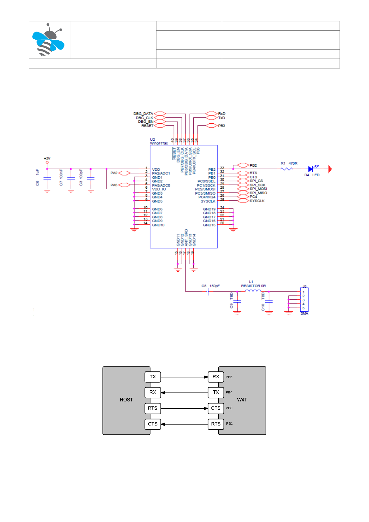
Communication between the host controller and Wing4TRAX module is based on a standard UART working
in half-duplex mode, as illustrated below:
Default factory UART setup is 19200 bauds, no parity, 8 data bits and 1 stop bit
By default, hardware flow control thru RTS/CTS handshaking signals is deactivated and RTS signal is set to 0
after reset; in this case, PB0 pin can be used as a general purpose input and PB1 as output
RTS/CTS handling can be activated thanks to a specific command issued by the host and RTS signal is set to
1 after reset; in this case PB0 and PB1 pins are reserved and driven by Wing4TRAX kernel
TRAXENS SAS – Les Baronnies – Bâtiment C – 15 Rue Marc Donadille – 13453 Marseille – France
SIRET 750 626 871 00016 ⎜APE 3320C ⎜Bureau : +33 4 91 11 88 16 ⎥ e-mail : info@traxens.com
Page 11

TRAX-Net module
Doc Reference
DSE-WING4TRAX OEM-User Manual
Page
11 / 33
DSE
Version/Revision
1.4
Date
20/07/2016
User’s manual
Security
Level 1 – Restricted
Name
SPI
I2C
IN
OUT
PC0
SS
-
PC1
SCK
-
PC2
MOSI
-
PC3
MISO
-
PC4
-
SDA
EXT_IRQ
SYSCLK
-
SCL
-
Frame format in both directions is as follows:
Communication protocol details can be found in specification [R1]
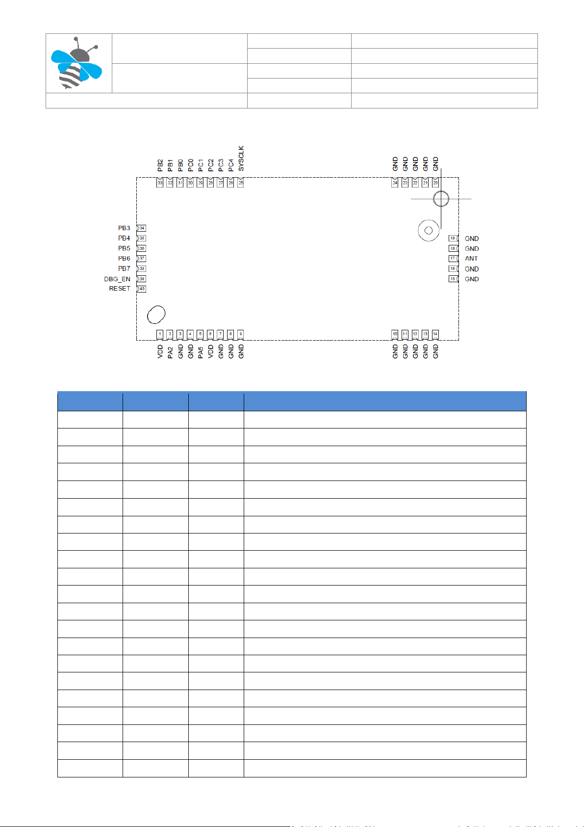
2.3 ANTENNA
ANT pin must be connected to a single pole antenna via a ceramic capacitor to avoid DC coupling with GND
A capacitor value between 100pF and 220pF (150pF typical) is commonly used
An additional inductance can be mounted between ANT pin and the capacitor to improve impedance
matching with the chosen antenna, as well as two foot capacitors to build a filter if extra filtering is
required. Feel free to contact us if you need more information about antenna design
2.4 GPIOS
Wing4TRAX offers a large panel of GPIOs on both ports B and C
Port B mapping is statically defined by the kernel, with 2 inputs and 4 outputs (UART RXD & TXD not
counted), meaning that direction of signal cannot be changed by the user; level change on PB0 and PB3
can be sensed by the kernel which generates events intercepted by user application. PB3, when tied low, is
also the sole pin by which the Wing4TRAX can exit the minimum consumption mode (DEEPSLEEP)
Port C & SYSCLK mapping can be dynamically defined by user application, with the possibility to interface
multiple slave devices, thru SPI bus and/or I2C bus, or thru discrete lines; the following table lists possible
alternate functions for port C & SYSCLK user pins:
SYSCLK is a special function pin, giving the opportunity to output permanent states 0 or 1 (0Hz clock), a
software programmable clock (e.g. 100KHz for I2C bus) or a hardware XTAL clock @32.768KHz with a
precision of +/-20ppm at @+25°C
TRAXENS SAS – Les Baronnies – Bâtiment C – 15 Rue Marc Donadille – 13453 Marseille – France
SIRET 750 626 871 00016 ⎜APE 3320C ⎜Bureau : +33 4 91 11 88 16 ⎥ e-mail : info@traxens.com
Page 12

TRAX-Net module
Doc Reference
DSE-WING4TRAX OEM-User Manual
Page
12 / 33
DSE
Version/Revision
1.4
Date
20/07/2016
User’s manual
Security
Level 1 – Restricted
2.5 ADC
Wing4TRAX features 2 external channels of analog-to-digital conversion on Port A pins PA2 and PA5
Conversion full scale is achieved with 1V voltage, and in any case, voltage applied on these pins shall not
exceed power supply voltage applied on VDD (pins 1 and 6)
In addition, Wing4TRAX provides 2 internal channels for application supervision:
An embedded temperature sensor with a precision of +/-2°C, over the full temperature range
Voltage applied on VDD pin calculated using the following formula:
VDD_Value = (ADC_Value x 0.0390625) – 4.5
Even if all conversions are performed with 10 bits resolution, the 2 LSBs are shifted out and results are
transferred to the application in 8 bits format (signed for temperature and unsigned for others)
2.6 SPI
SPI interface is only available in the configuration where the Wing4TRAX is the bus master
Slave Select (SS) signal is fully controlled by application, because active/inactive voltage to be applied to the
Chip Select (CS) pin varies with slave device manufacturer; if more than one SPI device must be interfaced,
free Port B outputs can be used too, as well as PC4 and SYSCLK, but with I2C interface exclusion
SPI clock can reach up to 5MHz and Wing4TRAX implements by default a clock setup without inversion (0V
when inactive) and MOSI/MISO data lines latch on clock rising edge; other setup is available on demand, as
illustrated below:
2.6 I2C
I2C interface is only available in the configuration where the Wing4TRAX is the bus master
Optionally, SCL and SDA lines can be internally pulled up with 65K, but most of the time this value is too
weak for normal bus operation under VDD voltage and external resistors are required
I2C clock signal SCL can reach up to 200KHz
2.7 EXT_IRQ
If not used by I2C interface, PC4 pin is available as an external interrupt source
EXT_IRQ function is sensitive to rising or falling edges of signal applied to pin PC4, and each change can be
intercepted by the Wing4TRAX kernel and notified to the application thanks to EXTIRQ_EVENT
TRAXENS SAS – Les Baronnies – Bâtiment C – 15 Rue Marc Donadille – 13453 Marseille – France
SIRET 750 626 871 00016 ⎜APE 3320C ⎜Bureau : +33 4 91 11 88 16 ⎥ e-mail : info@traxens.com
Page 13

TRAX-Net module
Doc Reference
DSE-WING4TRAX OEM-User Manual
Page
13 / 33
DSE
Version/Revision
1.4
Date
20/07/2016
User’s manual
Security
Level 1 – Restricted
Symbol
Description
Conditions
Min.
Max.
Unit
VDD
Supply voltage
-0.5
+5.5
V
IDD
Supply current
- 200
mA
P
WRT
Total power consumption
- 800
mW
P
WRA
Maximum input power on ANT pin
Wing4TRAX in RX mode
-
10
dBm
IDC
DC current into any pin except ANT
-10
+10
mA
I
OUT
Output current
- 40
mA
VDC
Input voltage any pin except ANT
-0.5
+5.5
V
T
AMB
Operating temperature
-40
+85
°C
T
STG
Storage temperature
-65
+150
°C
V
ESD
Electrostatic handling
-2
+2
kV
Symbol
Description
Conditions
Min.
Typ.
Max.
Unit
Supplies
T
AMB
Operational ambient temperature
-40
25
+85
°C
VDD
Power supply and I/O voltage
1.8
3.0
3.6
V
V
BOT
Brown-out threshold
- 1.3 - V
I
DSLEEP
Deep Sleep current
- 100
-
nA
I
SLEEP
Sleep current
8.25Kb RAM retained
-
2.2 - µA
I
STANDBY
Standby current
- 85 - µA
I
RUN
Microcontroller running current
- 3 - mA
I
RFRX
RF receiver consumption
- 9.5 - mA
I
RFTX
RF transmitter consumption
- 45 - mA
I
RFOSC
RF XTAL oscillator consumption
48MHz
-
500
-
µA
I
TMOSC
Time XTAL oscillator consumption
32.768KHz
-
700
-
nA
I
ADC
ADC current
312.5 ksample/s
-
1.1 - mA
I
WOR
Typical Wake-On-Radio duty cycle
360ms, 20Kbps
-
13.9
-
µA
Digital inputs
VT+
Schmitt trigger low to high threshold
VDD = 3.0V
-
1.4 - V
VT-
Schmitt trigger high to low threshold
-
1.13 - V
VIL
Input voltage low
- - 0.8
V
VIH
Input voltage high
2.0 - -
V
V
IPA
Input voltage range port A
-0.5
-
VDD
V
V
IPBC
Input voltage range ports B and C
-0.5 - 5.5
V
IL
Input leakage current
-10 - +10
µA
R
IPU
Programmable internal pull-up resistor
- 65 - k
3 HARDWARE INTERFACES
3.1 ABSOLUTE MAXIMUM RATINGS
Stresses above those listed values below may cause permanent damage to the device
Exposure to absolute maximum rating conditions for extended periods may affect device reliability
3.2 DC CHARACTERISTICS
TRAXENS SAS – Les Baronnies – Bâtiment C – 15 Rue Marc Donadille – 13453 Marseille – France
SIRET 750 626 871 00016 ⎜APE 3320C ⎜Bureau : +33 4 91 11 88 16 ⎥ e-mail : info@traxens.com
Page 14

TRAX-Net module
Doc Reference
DSE-WING4TRAX OEM-User Manual
Page
14 / 33
DSE
Version/Revision
1.4
Date
20/07/2016
User’s manual
Security
Level 1 – Restricted
Digital outputs
I
OHPBC
Output current high ports B and C
VOH = 2.4V
8 - -
mA
I
OLPBC
Output current low ports B and C
VOL = 0.4V
8 - -
mA
I
OHSYSCLK
Output current high SYSCLK pin
VOH = 2.4V
4 - -
mA
I
OLSYSCLK
Output current low SYSCLK pin
VOL = 0.4V
4 - -
mA
IOZ
Tri-states output leakage current
-10 - +10
µA
Analog inputs
F
ADCSR
ADC sampling rate
30 500
kHz
F
ADCSRT
ADC sampling rate temperature sensor
10
15.6
30
kHz
B
ADCRES
ADC resolution
- 10 - Bits
C
IPA
Input capacitance on PA2 and PA5 pins
- -
2.5
pF
B
ADCERR
ADC non linearity error
-1 - +1
LSB
B
ADCOFF
ADC offset
- 3 - LSB
V
ADCFS
ADC full swing input
0 - 1 V
Temperature sensor
T
RNG
Temperature range
-40 - +85
°C
T
RES
Temperature resolution
- 0.1607
-
°C/LSB
T
ERR
Temperature error
-2 - +2
°C
Symbol
Description
Conditions
Min.
Typ.
Max.
Unit
Generic
P
TXRNG
Programmable transmitter power
50 measurement
-10 - +13
dBm
P
TXTEMP
Transmitter power drift versus T°
-40°C to +85°C
-0.5
-
+0.5
dB
P
TXVDD
Transmitter power drift versus VDD
1.8V to 3.6V
-0.5
-
+0.5
dB
F
IPRECS
Frequency absolute precision
@25°C
-10
-
+10
ppm
F
DTEMP
Frequency drift versus temperature
-40°C to +85°C
-15
-
+15
ppm
F
AGING
Frequency aging
1 year
-1 - +1
ppm
SBR
Signal bit rate
- 20 - Kbps
F
SKMI
Modulation index (GMSK)
- 0.5 - -
F
SKGBT
Gaussian pulse shaping
- 0.5 - -
F
CHSPACE
Channel spacing
AGFS dependent
100
-
250
KHz
F
CHNUM
Number of channels
12 - 68
-
433 MHz band
F
R433
Frequency range
433.05
-
434.79
MHz
P
TX433_2
Harmonic 2 TX power
See note 1
-
-37 - dBm
P
TX433_3
Harmonic 3 TX power
-
-34 - dBm
S
RX433_1
RX sensitivity @433.12 MHz
BER = 10-3
-
-108
-
dBm
S
RX433_2
RX sensitivity @433.92 MHz
-
-108
-
dBm
S
RX433_3
RX sensitivity @434.72 MHz
-
-109
-
dBm
B
RX433_1
RX blocking @433.92 MHz
Offset = +/-2 MHz
-
71 - dB
B
RX433_2
Offset = +/-10 MHz
-
86 - dB
3.3 RF CHARACTERISTICS
TRAXENS SAS – Les Baronnies – Bâtiment C – 15 Rue Marc Donadille – 13453 Marseille – France
SIRET 750 626 871 00016 ⎜APE 3320C ⎜Bureau : +33 4 91 11 88 16 ⎥ e-mail : info@traxens.com
Page 15

TRAX-Net module
Doc Reference
DSE-WING4TRAX OEM-User Manual
Page
15 / 33
DSE
Version/Revision
1.4
Date
20/07/2016
User’s manual
Security
Level 1 – Restricted
868 MHz band
F
R868
Frequency range
863
-
870
MHz
P
TX868_2
Harmonic 2 TX power
See note 2
-
-50 - dBm
P
TX868_3
Harmonic 3 TX power
-
-58 - dBm
S
RX868_1
RX sensitivity @863.05 MHz
BER = 10-3
-
-111.5
-
dBm
S
RX868_2
RX sensitivity @866.50 MHz
-
-113
-
dBm
S
RX868_3
RX sensitivity @869.95 MHz
-
-112.5
-
dBm
B
RX868_1
RX blocking @866.5 MHz
Offset = +/-2 MHz
-
71 - dB
B
RX868_2
Offset = +/- 10 MHz
-
85 - dB
915 MHz band
F
R915
Frequency range
902
-
928
MHz
P
TX915_2
Harmonic 2 TX power
See note 3
-
38
-
dBµV/m
P
TX915_3
Harmonic 3 TX power
-
45
-
dBµV/m
S
RX915_1
Sensitivity @915.05 MHz
BER = 10-3
-
-112
-
dBm
S
RX915_2
Sensitivity @918.275 MHz
BER = 10-3
-
-111
-
dBm
S
RX915_3
Sensitivity @921.50 MHz
BER = 10-3
-
-110
-
dBm
S
RX915_4
Sensitivity @924.725 MHz
BER = 10-3
-
-109
-
dBm
S
RX915_5
Sensitivity @9271.95 MHz
BER = 10-3
-
-108
-
dBm
B
RX915_1
RX blocking @921.5 MHz
Offset = +/-2 MHz
-
70 - dB
B
RX915_2
Offset = +/- 10 MHz
-
84 - dB
Miscellaneous
P
RXWKP
RX wake-up period
- 360 - ms
D
TXPRMB
TX preamble duration
- -
390
ms
R
PAYLOAD
Effective payload rate (throughput)
Per second
1.1
KByte
Note 1: EN 300 220-2 measurement conditions §7.8.2.1, at 867.84 MHz for harmonic 2 and 1.30176 GHz for
harmonic 3 (433.92 MHz carrier power set at +13dBm)
Note 2: EN 300 220-2 measurement conditions §7.8.2.1, at 1.733 GHz for harmonic 2 and 2.5995 GHz for
harmonic 3 (866.5 MHz carrier power set at +13dBm)
Note 3: FCC part 15.247 test method (15.109, 15.209, 15.215b, 15.247), at 1.843 GHz for harmonic 2 and
2.764 GHz for harmonic 3 (921.5 MHz carrier measured with 114 dBµV/m at 3m)
TRAXENS SAS – Les Baronnies – Bâtiment C – 15 Rue Marc Donadille – 13453 Marseille – France
SIRET 750 626 871 00016 ⎜APE 3320C ⎜Bureau : +33 4 91 11 88 16 ⎥ e-mail : info@traxens.com
Page 16

TRAX-Net module
Doc Reference
DSE-WING4TRAX OEM-User Manual
Page
16 / 33
DSE
Version/Revision
1.4
Date
20/07/2016
User’s manual
Security
Level 1 – Restricted
3.4 MECHANICAL CHARACTERISTICS
Mechanical tolerances:
PCB dimensions on X & Y axis: +/- 0.2 mm
PCB + shield thickness: +/- 0.4 mm
Pad position and size: +/- 0.05 mm
TRAXENS SAS – Les Baronnies – Bâtiment C – 15 Rue Marc Donadille – 13453 Marseille – France
SIRET 750 626 871 00016 ⎜APE 3320C ⎜Bureau : +33 4 91 11 88 16 ⎥ e-mail : info@traxens.com
Figure 2: mechanical dimensions
Page 17

TRAX-Net module
Doc Reference
DSE-WING4TRAX OEM-User Manual
Page
17 / 33
DSE
Version/Revision
1.4
Date
20/07/2016
User’s manual
Security
Level 1 – Restricted
3.5 FOOTPRINT CHARACTERISTICS
Layout precautions: module bottom layer in contact with host PCB must be considered as a
KEEP OUT area; except for host pads, avoid copper plan, tracks and via on the host PCB layer in
contact with the module
Note: KiCAD or ALTIUM Designer footprints are available on request
Figure 3: footprint dimensions
TRAXENS SAS – Les Baronnies – Bâtiment C – 15 Rue Marc Donadille – 13453 Marseille – France
SIRET 750 626 871 00016 ⎜APE 3320C ⎜Bureau : +33 4 91 11 88 16 ⎥ e-mail : info@traxens.com
Page 18

TRAX-Net module
Doc Reference
DSE-WING4TRAX OEM-User Manual
Page
18 / 33
DSE
Version/Revision
1.4
Date
20/07/2016
User’s manual
Security
Level 1 – Restricted
4 DECLARATIONS OF CONFORMITY
The gain of the system antenna(s) used with Wing4TRAX (i.e. the combined transmission line,
connector, cable losses and radiating element gain) must not exceed 6dBi (in 433 MHz, 868 MHz
and 915 MHz bands) for mobile and fixed or mobile operating configurations.
4.1 R&TTE CONFORMITY FOR 433 MHZ AND 863 MHZ BANDS
Name: Wing4TRAX
Reference: W4T-V1.0-REV.F
This device complies with EN 300 220-1 v2.4.1 and EN 300 220-2 v2.4.1
According to the R&TTE Directive (1999/5/CE)
4.2 FCC CONFORMITY FOR 915 MHZ BAND
This RF module (Model: WING4TRAX – FCC ID: 2AHZ6WING4TRAX) is limited to OEM installation only, in
mobile or fixed applications; separate approval is required for all other operating configurations, including
portable configuration with respect to Part 2.1093
It can only be used in devices certified by TRAXENS under the following conditions:
The antenna(s) must be installed such that a minimum separation distance of 20cm is maintained
between the antenna and user’s/nearby person’s body at all times
The device must not be co-located with any other antenna or transmitter
OEM integrators shall not provide installation and/or removal instructions to end-users.
End-user’s operating manual delivered with finished products shall include the following information:
This device complies with Part 15 of the FCC Rules. Operation is subject to the following two conditions:
(1) This device may not cause harmful interference, and
(2) This device must accept any interference received, including interference that may cause undesired
operation
Finished products integrating this RF module (Model: WING4TRAX) shall bear the following label:
This device contains RF module (FCC ID: 2AHZ6WING4TRAX)
Prior to any distribution or installation, all products integrating the Wing4TRAX module shall be certified by
TRAXENS; changes or modifications applied afterwards and not expressly approved by TRAXENS SAS could
void the user's authority to operate the equipment.
Note: the grantee is not responsible for any changes or modifications not expressly approved by the party
responsible for compliance. Such modifications could void the user’s authority to operate the equipment
TRAXENS SAS – Les Baronnies – Bâtiment C – 15 Rue Marc Donadille – 13453 Marseille – France
SIRET 750 626 871 00016 ⎜APE 3320C ⎜Bureau : +33 4 91 11 88 16 ⎥ e-mail : info@traxens.com
Page 19

TRAX-Net module
Doc Reference
DSE-WING4TRAX OEM-User Manual
Page
19 / 33
DSE
Version/Revision
1.4
Date
20/07/2016
User’s manual
Security
Level 1 – Restricted
4.3 CSA CONFORMITY FOR 915 MHZ BAND
Canada, Industry Canada (IC) Notices
This device complies with Industry Canada license-exempt RSS-210 standard(s). Operation is subject to the
following two conditions:
This device may not cause interference, and
This device must accept any interference, including interference that may cause undesired
operation of the device
Radio Frequency (RF) Exposure Information
The radiated output power of the Wing4TRAX Module is below the Industry Canada (IC) radio frequency
exposure limits. The Wing4TRAX Module should be used in such a manner such that the potential for human contact during normal operation is minimized.
This device has been evaluated and shown compliant with the IC RF Exposure limits under mobile exposure
conditions (antennas are greater than 20cm from a person's body).
IMPORTANT: Manufacturers of portable applications incorporating the Wing4TRAX module are required to
have their final product certified and apply for their own FCC Grant and Industry Canada Certificate related
to the specific portable device. This is mandatory to meet the SAR requirements for portable devices.
Changes or modifications not expressly approved by the party responsible for compliance could void the
user's authority to operate the equipment.
Canada, avis d'Industrie Canada (IC)
Cet appareil numérique de classe B est conforme aux normes canadiennes RSS-210. Son fonctionnement
est soumis aux deux conditions suivantes:
cet appareil ne doit pas causer d'interférence
cet appareil doit accepter toute interférence, notamment les interférences qui peuvent affecter son
fonctionnement
Informations concernant l'exposition aux fréquences radio (RF)
La puissance de sortie émise par l’appareil sans fil Wing4TRAX Module est inférieure à la limite d'exposition
aux fréquences radio d'Industrie Canada (IC). Utilisez l’appareil sans fil Wing4TRAX Module de façon à minimiser les contacts humains lors du fonctionnement normal.
Ce périphérique a été évalué et démontré conforme aux limites d'exposition aux fréquences radio (RF) d'IC
lorsqu'il est installé dans des produits hôtes particuliers qui fonctionnent dans des conditions d'exposition à
des appareils mobiles (les antennes se situent à plus de 20 centimètres du corps d'une personne).
IMPORTANT: les fabricants d'applications portables contenant le module Wing4TRAX doivent faire certifier
leur produit final et déposer directement leur candidature pour une certification FCC ainsi que pour un
certificat Industrie Canada délivré par l'organisme chargé de ce type d'appareil portable. Ceci est obligatoire afin d'être en accord avec les exigences SAR pour les appareils portables.
Tout changement ou modification non expressément approuvé par la partie responsable de la certification
peut annuler le droit d'utiliser l'équipement
TRAXENS SAS – Les Baronnies – Bâtiment C – 15 Rue Marc Donadille – 13453 Marseille – France
SIRET 750 626 871 00016 ⎜APE 3320C ⎜Bureau : +33 4 91 11 88 16 ⎥ e-mail : info@traxens.com
Page 20

TRAX-Net module
Doc Reference
DSE-WING4TRAX OEM-User Manual
Page
20 / 33
DSE
Version/Revision
1.4
Date
20/07/2016
User’s manual
Security
Level 1 – Restricted
5 INTEGRATION GUIDELINES
5.1 DESIGN CHECKLIST
5.1.1 SCHEMATICS
The following are the most important points for a simple schematic check:
DC supply must provide a nominal voltage at VDD pins above the minimum operating range limit.
DC supply must be capable of providing up to 75 mA current, providing a voltage at VDD pins above
the minimum operating range limit and with a maximum 150 mV voltage drop from the nominal
value.
VDD supply should be clean, with very low ripple/noise: provide the suggested series ferrite bead
and bypass capacitors, in particular if the application device integrates an internal antenna.
VDD voltage must ramp from 0.1V maximum and then rise with a slope of at least 0.1V/ms to the
normal operating voltage.
Check that voltage level of any connected pin does not exceed the specific operating range.
Provide appropriate access to UART RxD and TxD lines for debugging (resp. PB5 and PB4).
Capacitance and series resistance must be limited on each line of the SPI interface, if the interface
is used.
Add a proper pull-up resistor to a proper supply on each I2C interface line, if the interface is used.
Capacitance and series resistance must be limited on each line of the I2C interface.
Connect all the pins referred as GND to the ground.
Provide proper precautions for ESD immunity as required on the application board.
Any external signal connected to the UART interface, SPI interface, I2C interface and GPIOs must be
tri-stated when the module is in power-down mode, when the external reset is forced low and during the module power-on sequence (at least for 100 ms after the start-up event), to avoid latch-up
of circuits and let a proper boot of the module.
All unused pins can be left floating on the application board, except the PB3 pin if the module has
to be put in DEEP_SLEEP mode
5.1.2 LAYOUT
The following are the most important points for a simple layout check:
Check 50 Ω nominal characteristic impedance of the RF transmission line connected to the ANT pad
(main RF input/output).
Follow the recommendations of the antenna producer for correct antenna installation and deploy-
ment (PCB layout and matching circuitry).
Ensure no coupling occurs with other noisy or sensitive signals (primarily SPI and/or I2C interfaces).
VDD line should be as wide and as short as possible (i.e. width of 0.25mm min.)
Provide the suggested series ferrite bead and bypass capacitors close to the VDD pins implement-
ing the recommended layout and placement, especially if the application device integrates an internal antenna.
Route VDD supply line away from sensitive analog signals.
Ensure proper grounding.
Consider “No-routing” areas for the Module footprint (see section § 3.5).
TRAXENS SAS – Les Baronnies – Bâtiment C – 15 Rue Marc Donadille – 13453 Marseille – France
SIRET 750 626 871 00016 ⎜APE 3320C ⎜Bureau : +33 4 91 11 88 16 ⎥ e-mail : info@traxens.com
Page 21

TRAX-Net module
Doc Reference
DSE-WING4TRAX OEM-User Manual
Page
21 / 33
DSE
Version/Revision
1.4
Date
20/07/2016
User’s manual
Security
Level 1 – Restricted
Rank
Function
Pin(s)
Attention to pay
Remark
1st
RF antenna
ANT
VERY HIGH
Design for 50 Ω characteristic impedance
2nd
Main DC supply
VDD
HIGH
VDD line should be wide and short.
Route away from sensitive analog signals
3rd
Ground
GND
HIGH
Provide proper grounding
4th
Analog pins
PA2, PA5
HIGH
If ADC0 and/or ADC1 lines are used
Avoid coupling with noisy signals
5th
High-speed
digital pins
PC1..PC3
HIGH
If SCK, MOSI and MISO lines are used
Avoid coupling with sensitive signals
6th
Digital pins &
supplies
PB0..PB7,
PC0, PC4,
SYSCLK,
DBG_EN,
RESET_N
Medium
Follow common practice rules for digital pin
routing
Optimize placement for minimum length of RF line and closer path from DC source for VDD.
Keep routing short and minimize parasitic capacitance on the SPI lines to preserve signal integrity.
5.1.3 ANTENNA
Antenna should have a 50 Ω impedance, VSWR less than 3:1 (recommended 2:1) on operating
bands in deployment geographical area.
Follow the recommendations of the antenna producer for correct antenna installation and deploy-
ment (PCB layout and matching circuitry).
Follow the additional guidelines for products marked with the FCC logo (United States only) report-
ed in section §5.2
The antenna connected to the ANT pad should be DC isolated with a ceramic COG/NPO capacitor of
150pF.
5.2 LAYOUT RECOMMENDATIONS
5.2.1 GUIDELINES PER PIN FUNCTION
The following design guidelines must be met for optimal integration of Wing4TRAX module on the final
application board
5.2.2 RF ANTENNA CONNECTION
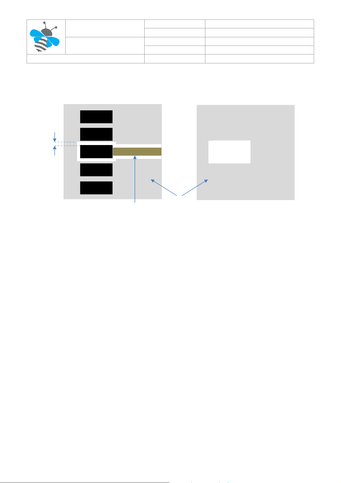
The ANT pin provided by Wing4TRAX module is very critical in layout design.
Proper transition between ANT pad and the application board must be provided, implementing the following design-in guidelines for the layout of the application PCB close to the ANT pad:
On a multi-layer board, the whole layer stack below the RF connection should be free of digital lines
Increase GND keep-out (i.e. clearance) for ANT pad to at least 175 μm up to adjacent pads metal
definition, as described in Figure 4
Add GND keep-out (i.e. clearance) on buried metal layers below ANT pad and below any other pad
of component present on the RF line, if top-layer to buried layer dielectric thickness is below 200
TRAXENS SAS – Les Baronnies – Bâtiment C – 15 Rue Marc Donadille – 13453 Marseille – France
SIRET 750 626 871 00016 ⎜APE 3320C ⎜Bureau : +33 4 91 11 88 16 ⎥ e-mail : info@traxens.com
Page 22
TRAX-Net module
Doc Reference
DSE-WING4TRAX OEM-User Manual
Page
22 / 33
DSE
Version/Revision
1.4
Date
20/07/2016
User’s manual
Security
Level 1 – Restricted
Top Layer
Ground
Buried metal Layer
175µm min.
Microstrip line 50 Ohm
μm, to reduce parasitic capacitance to ground (see Figure 4 for the description of the GND keep-out
area below ANT pad)
Figure 4: GND keep-out area on top layer around and on buried layer below ANT pad
The transmission line from the ANT pad up to antenna connector or up to the internal antenna pad must
be designed so that the characteristic impedance is as close as possible to 50 Ω.
The transmission line up to antenna connector or pad may be a microstrip (consists of a conducting
strip separated from a ground plane by a dielectric material) or a strip line (consists of a flat strip of
metal which is sandwiched between two parallel ground planes within a dielectric material). In any
case must be designed to achieve 50 Ω characteristic impedance
Microstrip lines are usually easier to implement and the reduced number of layer transitions up to
antenna connector simplifies the design and diminishes reflection losses. However, the electromagnetic field extends to the free air interface above the stripline and may interact with other circuitry
Buried striplines exhibit better shielding to external and internally generated interferences. They
are therefore preferred for sensitive application. In case a stripline is implemented, carefully check
that the via pad-stack does not couple with other signals on the crossed and adjacent layers
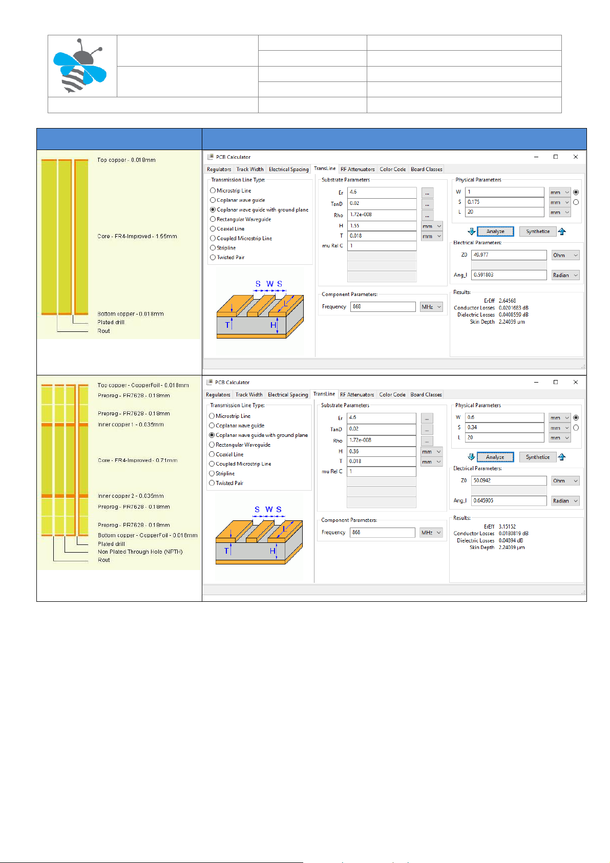
Figures 5 below provide two examples of proper 50 Ω coplanar waveguide designs. The first transmission
line can be implemented in case of 2-layer PCB stack-up herein described, the second transmission line can
be implemented in case of 4-layer PCB stack-up herein described:
With a 2-layer PCB stack using FR-4 material (
layers, 18µm of copper thickness for the top layer, a 50 Ω microstrip line can be achieved with a line
of 1.0mm width and a clearance of 0.175mm from GND
With a 4-layer PCB stack using FR-4 material (
layers, 18µm of copper thickness for the top layer, a 50 Ω microstrip line can be achieved with a line
of 0.6mm width and a clearance of 0.34mm from GND
TRAXENS SAS – Les Baronnies – Bâtiment C – 15 Rue Marc Donadille – 13453 Marseille – France
SIRET 750 626 871 00016 ⎜APE 3320C ⎜Bureau : +33 4 91 11 88 16 ⎥ e-mail : info@traxens.com
= 4.6) of 1.55mm height between top and bottom
r
= 4.6) of 0.36mm height between top and first inner
r
Page 23
TRAX-Net module
Doc Reference
DSE-WING4TRAX OEM-User Manual
Page
23 / 33
DSE
Version/Revision
1.4
Date
20/07/2016
User’s manual
Security
Level 1 – Restricted
Board buildup
Coplanar waveguide transmission line parameters
Figure 5: 50 Ω coplanar waveguide transmission line calculation with different PCB buildup
If the two examples do not match the application PCB layup, the 50 Ω characteristic impedance calculation
can be made using the HFSS commercial finite element method solver for electromagnetic structures from
ANSYS Corporation, or using freeware tools like AppCAD from Agilent or TXLine from Applied Wave Research, taking care of the approximation formulas used by the tools for the impedance computation.
To achieve a 50 Ω characteristic impedance, the width of the transmission line must be chosen depending
on:
the thickness of the transmission line itself (e.g. 18 μm in the example of Figure 5)
the thickness of the dielectric material between the top layer (where the transmission line is rout-
ed) and the inner closer layer implementing the ground plane (e.g. 360 μm or 1550 μm in Figure 5)
TRAXENS SAS – Les Baronnies – Bâtiment C – 15 Rue Marc Donadille – 13453 Marseille – France
SIRET 750 626 871 00016 ⎜APE 3320C ⎜Bureau : +33 4 91 11 88 16 ⎥ e-mail : info@traxens.com
Page 24

TRAX-Net module
Doc Reference
DSE-WING4TRAX OEM-User Manual
Page
24 / 33
DSE
Version/Revision
1.4
Date
20/07/2016
User’s manual
Security
Level 1 – Restricted
the dielectric constant of the dielectric material (e.g. dielectric constant of the FR-4 dielectric mate-
rial in Figure 5 given at r = 4.6)
the gap from the transmission line to the adjacent ground plane on the same layer of the transmis-
sion line (e.g. 175 μm or 340 μm in Figure 5)
Additionally to the impedance matching at 50 Ω, the following guidelines are recommended for the RF line
design:
Minimize the transmission line length; the insertion loss should be minimized as much as possible,
in the order of a few tenths of a dB
The transmission line should not have abrupt change to thickness and spacing to GND, but must be
uniform and routed as smoothly as possible
The transmission line must be routed in a section of the PCB where minimal interference from
noise sources can be expected
Route RF transmission line far from other sensitive circuits as it is a source of electromagnetic inter-
ference
Avoid coupling with VDD routing and analog lines
Ensure solid metal connection of the adjacent metal layer on the PCB stack-up to main ground layer
Add GND via around transmission line (e.g. repetitive pattern of via spaced by 2.54mm)
Ensure no other signals are routed parallel to transmission line, or that other signals cross on adja-
cent metal layer
If the distance between the transmission line and the adjacent GND area (on the same layer) does
not exceed 5 times the track width of the microstrip, use the “Coplanar Waveguide” model for 50 Ω
characteristic impedance calculation
Do not route microstrip line below discrete component or other mechanics placed on top layer
When terminating transmission line on antenna connector (or antenna pad) it is very important to
strictly follow the connector manufacturer’s recommended layout
GND layer under RF connectors and close to buried via should be cut out in order to remove stray
capacitance and thus keep the RF line 50 Ω. In most cases the large active pad of the integrated antenna or antenna connector needs to have a GND keep-out (i.e. clearance) at least on first inner
layer to reduce parasitic capacitance to ground. Note that the layout recommendation is not always
available from connector manufacturer: e.g. the classical SMA Pin-Through-Hole needs to have
GND cleared on all the layers around the central pin up to annular pads of the four GND posts.
Ensure no coupling occurs with other noisy or sensitive signals
Additional guidelines for products marked with the FCC logo - United States only
Wing4TRAX module can only be used with a host antenna circuit trace layout according to these guidelines; a host system designer must follow the guidelines to keep the original Grant of Wing4TRAX module.
Strict compliance to the layout reference design already approved (described in the following guidelines) is
required to ensure that only approved antenna shall be used in the host system.
If in a host system there is any difference from the trace layout already approved, it requires a Class II
permissive change or a new grant as appropriate as FCC defines.
Compliance of this device in all final host configurations is the responsibility of the Grantee.
The approved reference design for Wing4TRAX modules has a structure of 2 layers described below.
TRAXENS SAS – Les Baronnies – Bâtiment C – 15 Rue Marc Donadille – 13453 Marseille – France
SIRET 750 626 871 00016 ⎜APE 3320C ⎜Bureau : +33 4 91 11 88 16 ⎥ e-mail : info@traxens.com
Page 25
TRAX-Net module
Doc Reference
DSE-WING4TRAX OEM-User Manual
Page
25 / 33
DSE
Version/Revision
1.4
Date
20/07/2016
User’s manual
Security
Level 1 – Restricted
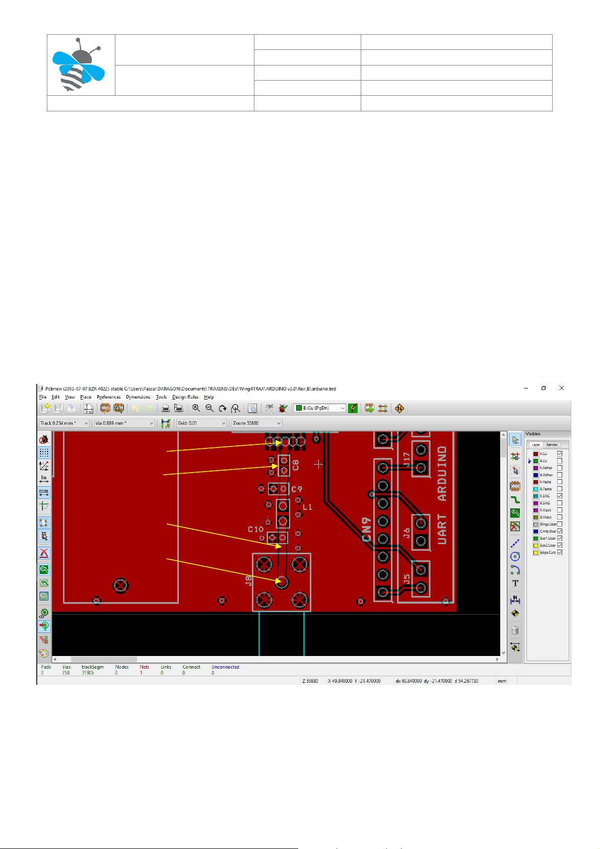
ANT pin pad
150pF capacitor
Microstrip line
Antenna connector
The top layer provides a microstrip line to connect the ANT pin of the Wing4TRAX module to the antenna
connector. The ANT pin of the Wing4TRAX module must be soldered on the designed pad which is connected to the antenna connector by a microstrip. The characteristics of the microstrip line (coplanar wave
guide) are the following:
Thickness = 0.018 mm
Width = 1.0 mm
Length = 20 mm
Gap (signal to GND) = 0.175 mm
The microstrip line must be designed to achieve 50 Ω characteristic impedance
The dimensions of the microstrip line must be calculated in a host system according to PCB characteristics
provided by PCB manufacturer.
Additional coupling and filtering components between the ANT pin pad and the antenna connector shall be
placed all along the microstrip line, in a way that preserves as much as possible integrity of the line; a special attention must be paid to the placement of components mounted in parallel to the microstrip line in
order to avoid generation of unexpected stubs
Figure 6: Layer 1 (top layer) of TRAXENS approved interface board for Wing4TRAX module
The thickness of the dielectric from Layer 1 (top layer) to Layer 2 (bottom layer) is 1.55 mm.
The Layer 2 (bottom layer) is designed for signals routing, components placement and GND plane.
Layer 2 thickness is 0.018 mm.
TRAXENS SAS – Les Baronnies – Bâtiment C – 15 Rue Marc Donadille – 13453 Marseille – France
SIRET 750 626 871 00016 ⎜APE 3320C ⎜Bureau : +33 4 91 11 88 16 ⎥ e-mail : info@traxens.com
Page 26

TRAX-Net module
Doc Reference
DSE-WING4TRAX OEM-User Manual
Page
26 / 33
DSE
Version/Revision
1.4
Date
20/07/2016
User’s manual
Security
Level 1 – Restricted
Figure 7: Layer 2 (bottom layer) of TRAXENS approved interface board for Wing4TRAX module
The antenna gain must not exceed the levels reported in the section §4 introduction to preserve
the original TRAXENS FCC ID.
The antenna must be installed and operated with a minimum distance of 20 cm from all persons
and must not be co-located or operating in conjunction with any other antenna or transmitter.
Under the requirements of FCC Section 15.212(a)-iv, the module must contain a permanently at-
tached antenna, or contain a unique antenna connector, and be marketed and operated only with
specific antenna(s).
In accordance with FCC Section 15.203, the antenna should use a unique coupling connector to the
approved reference design for Wing4TRAX module, to ensure that the design will not be deployed
with antenna of different characteristic from the approved type.
The use of standard SMA type connector is not permitted, as its standard usage allows easy re-
placement of the attached antenna. However RP-SMA (Reverse-Polarized-SMA) connector type fulfills the minimum requirements to prevent exchangeability of antenna on the reference design.
TRAXENS SAS – Les Baronnies – Bâtiment C – 15 Rue Marc Donadille – 13453 Marseille – France
SIRET 750 626 871 00016 ⎜APE 3320C ⎜Bureau : +33 4 91 11 88 16 ⎥ e-mail : info@traxens.com
Page 27

TRAX-Net module
Doc Reference
DSE-WING4TRAX OEM-User Manual
Page
27 / 33
DSE
Version/Revision
1.4
Date
20/07/2016
User’s manual
Security
Level 1 – Restricted
Item
Recommendations
Impedance
50 Ω nominal characteristic impedance
Frequency Range
Wing4TRAX module supports 3 sub-GHz ISM bands:
1. 433.05.. 434.79MHz
2. 863.. 869 MHz
3. 902.. 928 MHz
Input Power
20mW peak
VSWR
<2:1 recommended, <3:1 acceptable
Return Loss
S11 < -10dB recommended, S11 < -6dB acceptable
5.3 ANTENNA CHARACTERISTICS
Antenna characteristics are essential for good functionality of the module. Antenna radiating performance
has direct impact on the reliability of connections over the Air Interface. A bad termination of the ANT pin
can result in poor performance of the module.
The following parameters should be checked:
Sub-GHz ISM bands antennas are typically available as:
Linear monopole: typical for fixed applications (e.g. TRAX-Net gateway). The antenna extends most-
ly as a linear element with a dimension comparable to /4 of the lowest frequency of the operating
band. Magnetic base may be available. Cable or direct RF connectors are common options. The integration normally requires the fulfillment of some minimum guidelines suggested by antenna
manufacturer
PIFA: typical for mobile applications (e.g. TRAX-Box mounted onto a container). It consists of a
monopole antenna running parallel to a ground plane and grounded at one end. The antenna is fed
from an intermediate point a distance from the grounded end. The design has two advantages over
a simple monopole: the antenna is shorter and more compact, and the impedance matching can be
controlled by the designer without the need for additional matching components. However, the
design is complex and we recommend to rely on TRAXENS expertise in this field before considering
to implement this technology
Patch-like antenna: better suited for integration in compact designs (e.g. USB key). These are most-
ly custom designs where the exact definition of the PCB and product mechanical design is fundamental for tuning of antenna characteristics
For integration observe these recommendations:
Ensure 50 Ω antenna termination, minimize the V.S.W.R. or return loss, as this will optimize the
electrical performance of the module. See section §5.2.2
Select antenna with best radiating performance. See section §5.3.2
If a cable is used to connect the antenna radiating element to application board, select a short ca-
ble with minimum insertion loss. The higher the additional insertion loss due to low quality or long
cable, the lower the connectivity
Follow the recommendations of the antenna manufacturer for correct installation and deployment
Do not include antenna within closed metal case
TRAXENS SAS – Les Baronnies – Bâtiment C – 15 Rue Marc Donadille – 13453 Marseille – France
SIRET 750 626 871 00016 ⎜APE 3320C ⎜Bureau : +33 4 91 11 88 16 ⎥ e-mail : info@traxens.com
Page 28

TRAX-Net module
Doc Reference
DSE-WING4TRAX OEM-User Manual
Page
28 / 33
DSE
Version/Revision
1.4
Date
20/07/2016
User’s manual
Security
Level 1 – Restricted
Do not place the main antenna in close vicinity to end user since the emitted radiation in human
tissue is limited by S.A.R. regulatory requirements
Do not use directivity antenna since the electromagnetic field radiation intensity is limited in some
countries
Take care of interaction between co-located RF systems since the Wing4TRAX transmitted power
may interact or disturb the performance of companion systems
Place antenna far from sensitive analog systems or employ countermeasures to reduce electro-
magnetic compatibility issues that may arise
5.3.1 ANTENNA TERMINATION
The Wing4TRAX module is designed to work on a 50 Ω load. However, real antennas have no perfect 50 Ω
load on all the supported frequency bands. Therefore, to reduce as much as possible performance degradation due to antenna mismatch, the following requirements should be met:
With a network analyzer, connect the antenna through a coaxial cable to the measurement device;
S11 parameter indicates the power which is reflected by the antenna back to the module output.
A good antenna should have a S
below -10 dB over the entire frequency band. Due to miniaturiza-
11
tion, mechanical constraints and other design issues, this value may not be achieved; a S11 value of
about -6 dB is therefore acceptable.
Picture below shows an example of this measurement, with a good value of S11 in the 860-930MHz band
and an acceptable value in the 433MHz band (Frequency span = 150MHz, starting at 50MHz)
Figure 8: S11 measurement with a Nagoya NA-915-2 monopole antenna
TRAXENS SAS – Les Baronnies – Bâtiment C – 15 Rue Marc Donadille – 13453 Marseille – France
SIRET 750 626 871 00016 ⎜APE 3320C ⎜Bureau : +33 4 91 11 88 16 ⎥ e-mail : info@traxens.com
Page 29

TRAX-Net module
Doc Reference
DSE-WING4TRAX OEM-User Manual
Page
29 / 33
DSE
Version/Revision
1.4
Date
20/07/2016
User’s manual
Security
Level 1 – Restricted
Radiation patterns at 430-435-440 MHz
Radiation patterns at 860-900-930 MHz
5.3.2 ANTENNA RADIATION
An indication of the antenna’s radiated power can be approximated by measuring the S21 parameter from a
target antenna to the measurement antenna, using a network analyzer with a wideband antenna.
Measurements should be done at a fixed distance and orientation, and results compared to measurements
performed on a known good antenna.
For good antenna radiation performance, antenna dimensions should be comparable to a quarter of the
wavelength. Different antenna types can be used for the module, many of them (e.g. patch antennas,
monopole) are based on a resonating element that works in combination with a ground plane. The ground
plane, ideally infinite, can be reduced down to a minimum size that must be similar to one quarter of the
wavelength of the minimum frequency that has to be radiated (transmitted/received).
Numerical samples are given below (below calculated size, the antenna efficiency is reduced):
for a frequency = 450MHz wavelength = 66 cm minimum antenna size = 16.5 cm
for a frequency = 900MHz wavelength = 33 cm minimum antenna size = 8.3 cm
Picture below shows 3D radiation patterns for an omnidirectional antenna, designed to work over the 3
ISM bands, with a gain of 2dBi in lower band and 2.5dBi in upper bands:
Figure 9: radiation patterns of PULSE RO3ISMNM omnidirectional & wideband antenna
TRAXENS SAS – Les Baronnies – Bâtiment C – 15 Rue Marc Donadille – 13453 Marseille – France
SIRET 750 626 871 00016 ⎜APE 3320C ⎜Bureau : +33 4 91 11 88 16 ⎥ e-mail : info@traxens.com
Page 30

TRAX-Net module
Doc Reference
DSE-WING4TRAX OEM-User Manual
Page
30 / 33
DSE
Version/Revision
1.4
Date
20/07/2016
User’s manual
Security
Level 1 – Restricted
6 PRODUCT TESTING
6.1 TRAXENS MANUFACTURING TESTS
TRAXENS focuses on high quality for its products. All units produced are fully tested. Defective units are
analyzed in detail to improve the production quality.
This is achieved with automatic test equipment, which delivers a detailed test report for each unit. The
following measurements are done:
Digital self-test (firmware download, network UID and version information programming)
Measurement of voltages and currents in different power saving modes
Functional tests (serial interface communication, frame synchronization clock)
Digital tests (GPIOs, digital interfaces)
Analog tests (external ADCs, internal temperature sensor & reference voltage)
Measurement and calibration of RF characteristics in all supported bands (receiver sensitivity vs
BER, RSSI verification, tuning of frequency synthesizer, calibration of transmitter)
Verification of RF characteristics after calibration (power levels and spectrum performance are
checked to be within tolerances when calibration parameters are applied)
TRAXENS SAS – Les Baronnies – Bâtiment C – 15 Rue Marc Donadille – 13453 Marseille – France
SIRET 750 626 871 00016 ⎜APE 3320C ⎜Bureau : +33 4 91 11 88 16 ⎥ e-mail : info@traxens.com
Figure 10: Wing4TRAX manufacturing test bench
Page 31

TRAX-Net module
Doc Reference
DSE-WING4TRAX OEM-User Manual
Page
31 / 33
DSE
Version/Revision
1.4
Date
20/07/2016
User’s manual
Security
Level 1 – Restricted
controller
Wing4TRAX
ANT
Spectrum Analyser
IN
6.2 TESTS POLICY FOR OEM MANUFACTURER
Because of the testing done by TRAXENS with 100% coverage, an OEM manufacturer does not need to repeat firmware tests or measurements of the module RF performance or tests over analog and digital interfaces in their production test.
An OEM manufacturer should focus on:
Module assembly on the device; it should be verified that:
Soldering and handling process did not damaged the module components
All module pins are well soldered on the host board
There are no short circuits between pins
Component assembly on the device; it should be verified that:
Communication with host controller can be established
The interfaces between module and device are working (for those used)
RF performance tests of the device including antenna are conform to expectations
Dedicated tests can be implemented to check the device. For example, the measurement of module current consumption when set in a specified status can be performed to detect a short circuit when compared
with a “Golden Device” result.
Specific test commands [refer to R2] can be used to perform functional tests (communication with host
controller, reading of network UID, GPIOs, ADCs, etc.) and to perform RF performance tests.
6.2.1 “GO/NO GO” TESTS
A “GO/No GO” test is intended to simply compare the signal quality with a “Golden Device”, in a position
where it can communicate in P2P mode with another “Golden Device”, with a stable and well known level
of signal (refer to CMD_MAC_SHORT_SEND and CMD_MAC_GET_RSSI commands in R1)
This test is suitable to quickly check the communication between host controller and the Wing4TRAX
module, power-good functionality and RF path integrity from the module to the device antenna.
6.2.2 FUNCTIONAL RF TESTS
Overall RF performance test of the device including antenna can be performed with basic instruments such
as a spectrum analyzer (or RF power meter) and a signal generator using test commands [refer to R2].
The test command set gives a simple interface to set the module into TX and RX test modes, ignoring TRAXNet signaling protocol. Each command can set the module:
In transmitting mode, in a specified channel and power level without modulation
In receiving mode, in a specified channel to returns the measured power level
Host
TRAXENS SAS – Les Baronnies – Bâtiment C – 15 Rue Marc Donadille – 13453 Marseille – France
SIRET 750 626 871 00016 ⎜APE 3320C ⎜Bureau : +33 4 91 11 88 16 ⎥ e-mail : info@traxens.com
module
Or
Power Meter
Page 32

TRAX-Net module
Doc Reference
DSE-WING4TRAX OEM-User Manual
Page
32 / 33
DSE
Version/Revision
1.4
Date
20/07/2016
User’s manual
Security
Level 1 – Restricted
controller
Wing4TRAX
ANT
Signal Generator
OUT
Host
module
Figure 11: synoptic of OEM test platform for radiation measurement
This feature allows the measurement of the transmitter and receiver power levels to check component
assembly related to the module antenna interface and to check other device interfaces from which depends the RF performance.
To avoid module damage during transmitter test, a proper antenna according to module speci-
fications or a 50 Ω termination must be connected to ANT pin.
To avoid module damage during receiver test the maximum power level received at ANT pin
must meet module specifications.
Emission tests can generate interference that can be prohibited by law in some countries. The use
of this feature is intended for testing purpose in controlled environments by qualified user and
must not be used during the normal module operation.
Follow instructions suggested by TRAXENS documentation
TRAXENS assumes no responsibilities for the inappropriate use of this feature.
TRAXENS SAS – Les Baronnies – Bâtiment C – 15 Rue Marc Donadille – 13453 Marseille – France
SIRET 750 626 871 00016 ⎜APE 3320C ⎜Bureau : +33 4 91 11 88 16 ⎥ e-mail : info@traxens.com
Page 33

TRAX-Net module
Doc Reference
DSE-WING4TRAX OEM-User Manual
Page
33 / 33
DSE
Version/Revision
1.4
Date
20/07/2016
User’s manual
Security
Level 1 – Restricted
7 DISCLAIMERS
7.1 DOCUMENT STATUS
This manual is in initial version. Supplementary data will be published at a later date. TRAXENS reserves the
right to change its content without notice in order to improve the design and supply the best possible
product.
Please check with TRAXENS for the most recent data before initiating or completing a design.
Contact : support@traxens.com
7.2 ESD
Electronic semiconductor products are sensitive to Electro Static Discharge (ESD). Always observe Electro
Static Discharge control procedures whenever handling semiconductor products.
7.3 WARRANTY
TRAXENS warrants that its products shall conform to TRAXENS’s specifications and remain free from defects
materials and workmanship under normal, proper and intended use for a period of one (1) year from date
of purchase, provided that proof of purchase be furnished with any returned equipment.
7.4 DISPOSAL OF WASTE BY USERS IN PRIVATE HOUSEHOLDS WITHIN THE EUROPEAN UNION
This symbol on the product or on its packaging indicates that this product must not be disposed
off with your other household waste. Instead, it is your responsibility to dispose of your waste by
taking it to a collection point designated for the recycling of electrical and electronic appliances.
Separate collection and recycling of your waste at the time of disposal will contribute to conserving natural
resources and guarantee recycling that respects the environment and human health. For further information concerning your nearest recycling center, please contact your nearest local authority/town hall
offices, your household waste collection company or the distributor where you bought the product.
TRAXENS SAS – Les Baronnies – Bâtiment C – 15 Rue Marc Donadille – 13453 Marseille – France
SIRET 750 626 871 00016 ⎜APE 3320C ⎜Bureau : +33 4 91 11 88 16 ⎥ e-mail : info@traxens.com
 Loading...