

Page 1

UHC124 USB Host Controller
Data Sheet
TransDimension Inc.
2 Venture
Irvine, CA 92618
www.transdimension.com
Phone: (949) 727-2020
Fax: (949) 727-3232
sales@transdimension.com
techsupport@transdimension.com
TransDimension Document Number: MU1002
Rev. 1.05, February, 2002
Page 2

TransDimension Inc. UHC124 Data Sheet
Revision History
Version Number Release Date Notes
0.5 Aug., 1999 First release
0.75
Nov., 1999
• Changed UhcControl register
• Re-organized Interrupt Modes
• Moved batch interrupt control/status to
UhcInterruptEnable/UhcInterruptStatus
• Removed XDInterruptEnable field
• Pinout provided
• Added section on oscillator and PLL
• Added section on the root hub
• Added USB host state transition section
0.80 Dec., 1999
0.90 Jun., 2000
0.92 Jul., 2000
0.93
Aug., 2000
• Revised XDControl and XDStatus
• Revised all sections
• Added sections on interface and software
• Added chip pin assignment table and diagram
• Modified Sections 9 & 10 examples
• Modified electrical specifications for logic signals
0.95
Sept., 2000
• Changed pin assignments for DPn, DMn (n = 1, 2, 3,
and 4)
• Swapped Bits 7 & 5 of XDControl
0.97 Feb., 2001
0.98
Apr., 2001
• Made modifications for typos, etc.
• Modified legal statements
• Removed “Advanced Information”
• Removed “Confidential”
• Modified chip marking to match product
• Added a section on double buffering
• Corrected V
and VOL specifications
OH
• Corrected bus cycle specifications
• Added recommended landing pattern
• Added soldering profile
• Added storage conditions
1.00
May, 2001
• Corrected several typos
• Modified text on integrating the UHC124 to generic
USB host software
• Added/corrected electronic and timing specifications
• Corrected Maximum Absolute Ratings
• Added procedures of entering power save state
1.01 May, 2001
• Change “TDI Part Number:” on the cover page to
“TDI Document Number:”
1.02 August, 2001
1.03 Sept. 2001
1.04 October 2001
• Format change, added Sales Offices.
• Format change.
• Colorized the block diagram and updated feature list
TransDimension Inc. - Proprietary
Page 3

TransDimension Inc. UHC124 Data Sheet
1.04A December
• Updated sales contact list on last page.
2001
1.05 February
2002
• Refered readers to our website for all sales rep.
offices
Note: This data sheet is subject to change without notice.
TransDimension Inc. - Proprietary
Page 4

TransDimension Inc. UHC124 Data Sheet
THE DEVICE AND ITS DOCUMENTATION ARE PROVIDED “AS IS”.
TRANSDIMENSION HEREBY DISCLAIMS ALL WARRANTIES, EXPRESS,
STATUTORY AND IMPLIED, APPLICABLE TO THE SOFTWARE AND ITS
DOCUMENTATION AND ANY RELATED PRODUCTS, INCLUDING, BUT NOT
LIMITED TO, ANY WARRANTY OF MERCHANTABILITY, NON-INFRINGEMENT OR
FITNESS FOR A PARTICULAR PURPOSE. TRANSDIMENSION ASSUMES NO
LIABILITY FOR ANY ACT OR OMISSION OF LICENSEE. IN NO EVENT SHALL
TRANSDIMENSION BE LIABLE FOR DIRECT, SPECIAL, INDIRECT, INCIDENTAL,
PUNITIVE, EXEMPLARY OR CONSEQUENTIAL DAMAGES, INCLUDING, WITHOUT
LIMITATION, LOSS OF PROFITS OR REVENUE, LOSS OF PRODUCTS, DATA OR ANY
ASSOCIATED EQUIPMENT, COST OF CAPITAL, COST OF SUBSTITUTED EQUIPMENT
OR PARTS, FACILITIES OR SERVICES, DOWN-TIME OR LABOR COSTS, EVEN IF
TRANSDIMENSION HAS BEEN ADVISED OF THE POSSIBILITY THEREOF. The device
and any related products are not designed, authorized, or warranted to be suitable for use in lifesupport devices or systems or other critical applications. Any such use and subsequent liabilities
that may arise from such use are totally the responsibilities of the Licensee.
© 2002, TransDimension Inc., All rights reserved.
All product names are trademarks or registered trademarks of their respective owners.
TransDimension Inc. - Proprietary
Page 5

TransDimension Inc. UHC124 Data Sheet
Contents
1. Features and Block Diagram .................................................................................................. 1
1.1 Features of UHC124 ................................................................................................... 1
1.2 Block Diagram............................................................................................................ 2
1.3 Pin Assignments.......................................................................................................... 3
1.4 Abbreviations.............................................................................................................. 5
2. System Overview.................................................................................................................... 6
2.1 Interface with MCUs................................................................................................... 6
2.2 Control Memory and Transaction Descriptors ........................................................... 6
2.3 Batch Processing......................................................................................................... 7
2.4 Data Memory .............................................................................................................. 9
2.5 Double Buffering ........................................................................................................ 9
2.6 Interrupt to MCU ...................................................................................................... 10
2.7 Root Hub................................................................................................................... 10
2.8 External Crystal/Oscillator........................................................................................ 10
2.9 About UHCI and OHCI ............................................................................................ 10
2.10 USB Host API........................................................................................................... 11
2.11 RTOS Support........................................................................................................... 12
2.12 System Suspend and Resume.................................................................................... 12
2.13 Power Saving State ................................................................................................... 12
3. Signal Definitions................................................................................................................. 13
3.1 Oscillator and PLL.................................................................................................... 13
3.2 MCU Interface .......................................................................................................... 13
3.3 USB Root Hub Ports................................................................................................. 14
3.4 Test Modes................................................................................................................ 14
3.5 Power and Ground .................................................................................................... 14
4. Memory Map........................................................................................................................ 15
5. Control Registers.................................................................................................................. 16
5.1 Overview................................................................................................................... 16
5.2 UhcControl Register.................................................................................................. 16
5.3 UhcTransSelect Register........................................................................................... 20
5.4 UhcTransDone Register............................................................................................ 21
5.5 UhcIntpStatus Register ............................................................................................. 21
5.6 UhcIntpEnable Register............................................................................................ 23
5.7 UhcFmInterval Register............................................................................................ 24
5.8 UhcFmRemaining Register....................................................................................... 25
5.9 UhcFmNumber Register ........................................................................................... 25
5.10 UhcMaxOverhead Register....................................................................................... 26
5.11 UhcMagicNumber Register ...................................................................................... 26
6. Transaction Descriptor ......................................................................................................... 28
TransDimension Inc. - Proprietary i
Page 6

TransDimension Inc. UHC124 Data Sheet
6.1 Overview................................................................................................................... 28
6.2 XDControl................................................................................................................. 29
6.3 XDStatus................................................................................................................... 30
6.4 XDDevAddress ......................................................................................................... 31
6.5 XDEndpoint .............................................................................................................. 31
6.6 XDBufAddress.......................................................................................................... 32
6.7 XDBufLength ........................................................................................................... 32
6.8 XDXferCount............................................................................................................ 33
7. Root Hub .............................................................................................................................. 34
7.1 Down Stream Ports ................................................................................................... 34
7.2 Port Power Management........................................................................................... 34
7.3 Root Hub as a USB Device....................................................................................... 35
7.4 Hub Characteristics................................................................................................... 37
7.5 Port Manipulation ..................................................................................................... 38
7.6 Port Status Change Endpoint (EP1).......................................................................... 38
8. Host Controller Functional States ........................................................................................ 40
8.1 UHC124 States and State Transitions....................................................................... 40
8.2 UsbOperational ......................................................................................................... 41
8.3 UsbReset ................................................................................................................... 41
8.4 UsbSuspend............................................................................................................... 41
8.5 UsbResume ............................................................................................................... 42
8.6 PowerSave................................................................................................................. 42
9. Hardware Setup and Interface to MCU ................................................................................ 43
9.1 Power Supply............................................................................................................ 43
9.2 PowerOnReset and MasterReset............................................................................... 43
9.3 Crystal Oscillator ...................................................................................................... 43
9.4 Root Hub Ports.......................................................................................................... 44
9.5 Memory Access ........................................................................................................ 44
9.6 Test Modes................................................................................................................ 50
10. Software Issues..................................................................................................................... 51
10.1 Resets ........................................................................................................................ 51
10.2 Transaction Specification.......................................................................................... 52
10.3 Batch Dispatching..................................................................................................... 54
10.4 Transaction/Batch Scheduling .................................................................................. 54
10.5 Transaction Status Interpretation and Handling ....................................................... 55
10.6 USB Requests (Control Transfers) ........................................................................... 59
10.7 UHC124 Operation ................................................................................................... 60
10.8 Software Support ...................................................................................................... 63
11. Bus Cycle Timing................................................................................................................. 64
11.1 Memory Write Cycle ................................................................................................ 64
11.2 Memory Read Cycle ................................................................................................. 64
12. Electrical Ratings.................................................................................................................. 65
TransDimension Inc. - Proprietary ii
Page 7

TransDimension Inc. UHC124 Data Sheet
12.1 Absolute Maximum Ratings ..................................................................................... 65
12.2 Recommended/Normal Operating Conditions.......................................................... 65
12.3 D.C. Characteristics .................................................................................................. 65
12.4 A.C. Characteristics .................................................................................................. 66
13. Packaging, Soldering and Storage........................................................................................ 67
13.1 Package Diagram ...................................................................................................... 67
13.2 Packaging Dimensions.............................................................................................. 68
13.3 Landing Pattern......................................................................................................... 69
13.4 Soldering Profile ....................................................................................................... 70
13.5 Storage Conditions.................................................................................................... 70
14. Sales Offices:........................................................................................................................ 71
TransDimension Inc. - Proprietary iii
Page 8

TransDimension Inc. UHC124 Data Sheet
1. Features and Block Diagram
1.1 Features of UHC124
• USB host controller for embedded applications (set-top box, PDA, cell phone, digital camera,
Bluetooth USB HCI physical bus, etc.)
• USB Specification 2.0 (low and full speed) fully compliant
• Patent pending design
• Standard 8-bit microprocessor bus interface
• Supports batch processing of up to 16 USB transactions without interrupting the MCU
• Supports both full speed (12 Mbps) and low speed (1.5 Mbps) USB transfers
• Supports all four types of USB transfers (control, bulk, interrupt, and isochronous with
maximum packet size of 1023 bytes)
• Supports double and circular buffering for all four types of Host controller transactions
• Direct device-to-device data transfer in one Frame
• Separate transaction descriptor and data memory space
• Hardware generated Start of Frame (SOF)
• 2 KB data memory
• Support in-place processing in the data memory – used for applications requiring peer-to-
peer data transfer between USB devices
• Supports transaction spill over
• Power management with host suspend, remote wakeup, and power saving modes
• Fully qualified, market proven root hub with four downstream ports and integrated analog
transceivers
• Supports OHCI/UHCI compliant USB host stack
• USB device driver software available including printer, speaker, mass storage device, hub,
modem, ethernet, mouse, keyboard, digital camera, video camera, cell phone, STB, PDA, etc.
• Embedded RTOS software available for popular microprocessors, RISCs, CISCs, and DSPs
using WinCE, Linux, VxWorks, Nucleus, Lynx, QNX, pSOS, PowerTV, SMX, ThreadX,
VRTX, ITRON, MS-DOS operating systems
• 6 MHz crystal/oscillator to reduce cost and EMI
• Single 3.3V power supply
• Shipping industrial grade operating temperature range devices
• Military and Automotive grade available upon request
• 64 pin LQFP package
TransDimension Inc. - Proprietary
1
Page 9
TransDimension Inc. UHC124 Data Sheet
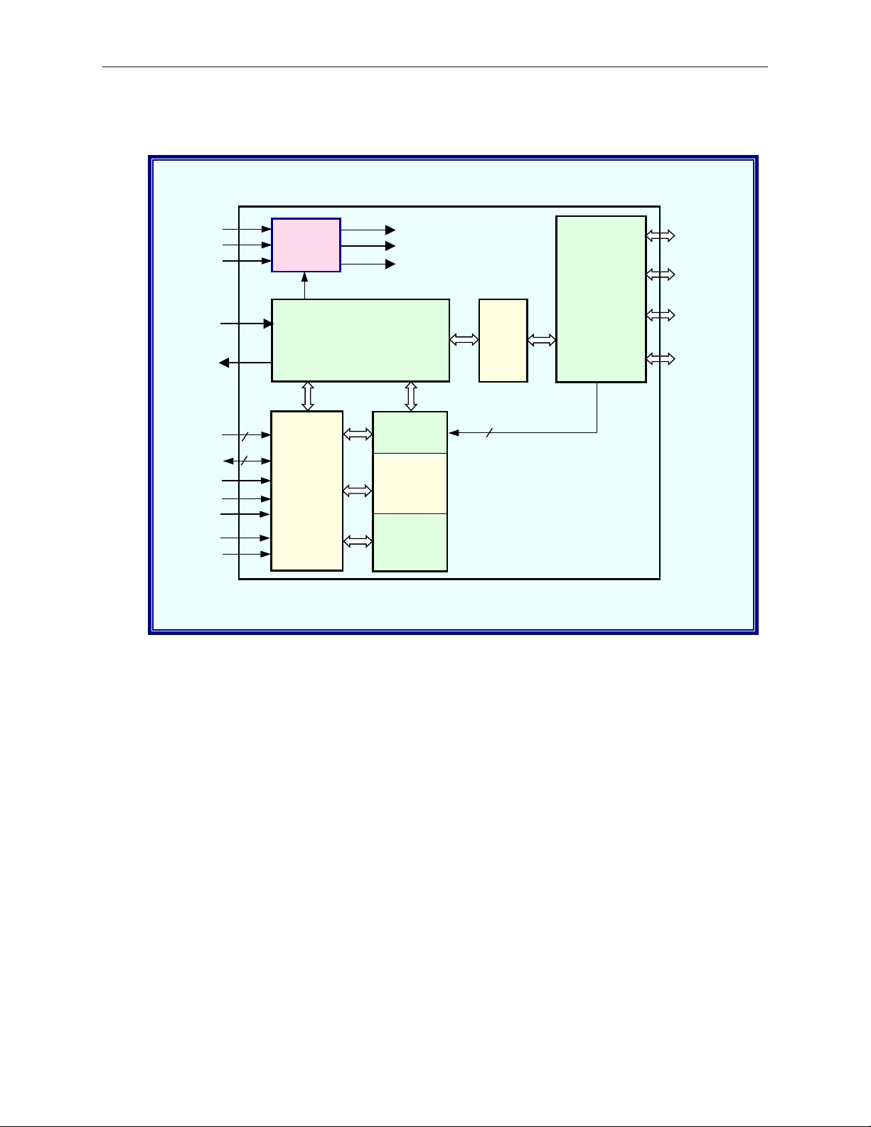
1.2 Block Diagram
OSC1
OSC
2
LPF
/RESET
A11..A0
..D0
D
7
/CS
/WR
/RD
ADS
MODE
12
8
PLL
PwrSav
Memory/
Register
Access
&
MCU
Interface
48MHz
12MHz
6MHz
USB Host
Control Logic
Registers
(16 Bytes)
Control
Memory
(256 Bytes)
Data
Memory
(2K Bytes)
5
Fig. 1 UHC124 block diagram
Host
SIE
PortChange[0:4]
Root Hub
With
Four
Downstream
Ports
DP1, DM1
/PO
, /OC
1
DP2, DM2
/PO
, /OC
2
DP3, DM3
/PO
, /OC
3
DP4, DM4
/PO
, /OC
4
1
2
3
4
TransDimension Inc. - Proprietary
2
Page 10

TransDimension Inc. UHC124 Data Sheet
1.3 Pin Assignments
1 V
17 OSC1 33 VDD 49 VSS
DD
2 A0 18 OSC2 34 DP1 50 D4
3 A1 19 LPF 35 DM1 51 D5
4 A2 20 VDD 36 VSS 52 D6
5 A3 21 TEST0 37 DP2 53 D7
6 A4 22 TEST1 38 DM2 54 /RESET
7 A5 23 TEST2 39 DP3 55 /WR
8 A6 24 TEST3 40 DM3 56 /RD
9 A7 25 /OC1 41 DP4 57 TMS0
10 A8 26 /OC2 42 DM4 58 TMS1
11 A9 27 /OC3 43 TEST4 59 TMS2
12 A10 28 /OC4 44 D0 60 TMS3
13 A11 29 /PO1 45 D1 61 /INT
14 MODE 30 /PO2 46 D2 62 ADS
15 /CS 31 /PO3 47 D3 63 GNDP
16 VSS 32 /PO4 48 VDD 64 VSS
TransDimension Inc. - Proprietary
3
Page 11
TransDimension Inc. UHC124 Data Sheet
DD
V
4
TEST
4
DM
3
2
D
D
1
0
D
D
4
DP
3
DM
3
DP
2
DM
2
DP
1
DM
DP
SS
V
1
DD
V
VSS
/RESET
/WR
/RD
TMS0
TMS1
TMS2
TMS3
/INT
ADS
GNDP
48 47 46 45 44 43 42 41 40 39 38 37 36 35 34 33
49 32
50 31
D4
51 30
D5
52 29
D6
53 28
D7
54 27
55 26
56 25
57 24
58 23
59 22
60 21
61 20
62 19
63 18
/PO4
/PO3
/PO2
/PO1
/OC4
/OC3
/OC2
/OC1
TEST3
TEST2
TEST1
TEST0
VDD
LPF
OSC2
VSS
64 17
1 2 3 4 5 6 7 8 9 10 11 12 13 14 15 16
■
0
1
2
3
4
5
6
7
8
DD
A
A
A
A
A
A
A
V
A
9
A
A
10
11
A
A
/CS
SS
V
MODE
Fig. 2 UHC124 LQFP 64-pin package (top view)
OSC1
TransDimension Inc. - Proprietary
4
Page 12

TransDimension Inc. UHC124 Data Sheet
1.4 Abbreviations
The following are some abbreviations used in this document.
API Application Programming Interface
CM Control Memory
DM Data Memory
FSBT Full Speed Bit Time
HC Host Controller
HCD Host Controller Driver
HCFS Host Controller Functional State
ISR Interrupt Service Routine
OHCI Open Host Controller Interface
PLL Phase Locked Loop
RTOS Real Time Operating System
SOF Start of Frame
UHCI Universal Host Controller Interface
XD Transaction Descriptor
TransDimension Inc. - Proprietary
5
Page 13

TransDimension Inc. UHC124 Data Sheet
2. System Overview
The UHC124 is a low-cost, high-performance, non-PCI USB host controller with unique, patentpending features that are indispensable for achieving high data throughput and low interrupt
rates. It is the only one on the market that is designed from the ground up for embedded
applications with full USB specification compliance. It is optimized for cost, performance and
ease of development. The software/hardware co-designed architecture enables high performance
while maintaining simplicity and flexibility that are critical for embedded applications. It can be
interfaced to CISC or RISC microprocessors, microcontrollers, or digital signal processors
(DSPs) and is ideal for providing USB host functions to a wide range of applications including
mobile devices, cell phones, PDAs, point-of-sale systems, test equipment, set-top boxes, Internet
appliances, as well as serving as an interface for USB to Bluetooth controllers.
TransDimension offers complete solutions using the UHC124 including development kits,
embedded USB host software and UHCI software interfaces to various real time operating
systems optimized for the UHC124. The complete solutions offer the advantages of shortened
time-to-market, simplified procurement and technical support from one source.
In the following, it is assumed that the reader has basic knowledge of microprocessor based
systems, as well as USB Specification 1.1. References to specific chapters and sections of USB
Specification 1.1 are cited in a pair of brackets. For instance, [9.3:183, 11.16:266] refers to “9.3
USB Device Request” on page 183, and “11.16 Requests” on page 266 of USB 1.1 Specification.
2.1 Interface with MCUs
UHC124 may be interfaced with a microprocessor-based system using either one of the two
following methods:
• For MCUs with standard external data buses, UHC124 can be interfaced directly via 8 bits of
its data bus and 12 bits of its address bus. When UHC124 operates under this mode, its
internal memory blocks, as well as its control/status registers, are mapped into the
processor’s address space.
• For MCUs without an external data bus, UHC124 may be interfaced using an 8-bit output
port and an 8-bit bi-directional port. Under this mode, a built-in, auto incrementing address
register allows accessing to a large block of UHC124 memory with a single (address) write
cycle, followed by as many read/write cycles as the number of data bytes to be transferred
from/to the UHC124.
Careful design of both hardware and software interfaces may allow a MCU with external data
buses to take advantage of UHC124’s auto-incremented addressing. See Section 9 for details.
2.2 Control Memory and Transaction Descriptors
The 256 bytes of Control Memory (CM) are evenly divided into 16 sections, each of which (16
bytes) specifies a Transaction Descriptor (XD) holding the following control information for a
USB transaction:
TransDimension Inc. - Proprietary
6
Page 14
TransDimension Inc. UHC124 Data Sheet
• Targeted USB device address (0-127) and endpoint number (0-15)
• Transaction type (SETUP, IN, or OUT)
• Starting address of the data block in UHC124 data memory
• Number of bytes to be transferred
• Whether the transaction is targeted to an isochronous endpoint
• Speed (data rate) of the targeted USB device
• Data sequence DATA0/1 (for an OUT transaction)
Upon completion of a transaction, the XD contains information about:
• Transaction status (Ack, Nak, Stall, Timeout, Error, or Overflow)
• Data sequence (for an IN transaction)
• Number of bytes actually transferred (for an IN transaction)
The sixteen XDs are hereafter referred to as XD0, XD1, …, XD9, XDA, XDB, …, XDE, and XDF.
2.3 Batch Processing
The Host Controller Driver (HCD) may organize up to 16 USB transactions into a transaction
batch, or simply a batch. A batch may contain transactions for full-speed (FS: 12 Mbit/sec) and
low-speed (LS: 1.5 Mbit/sec) USB devices, of four types of endpoints (control, bulk, interrupt
and isochronous) and all transaction types (SETUP, IN and OUT).
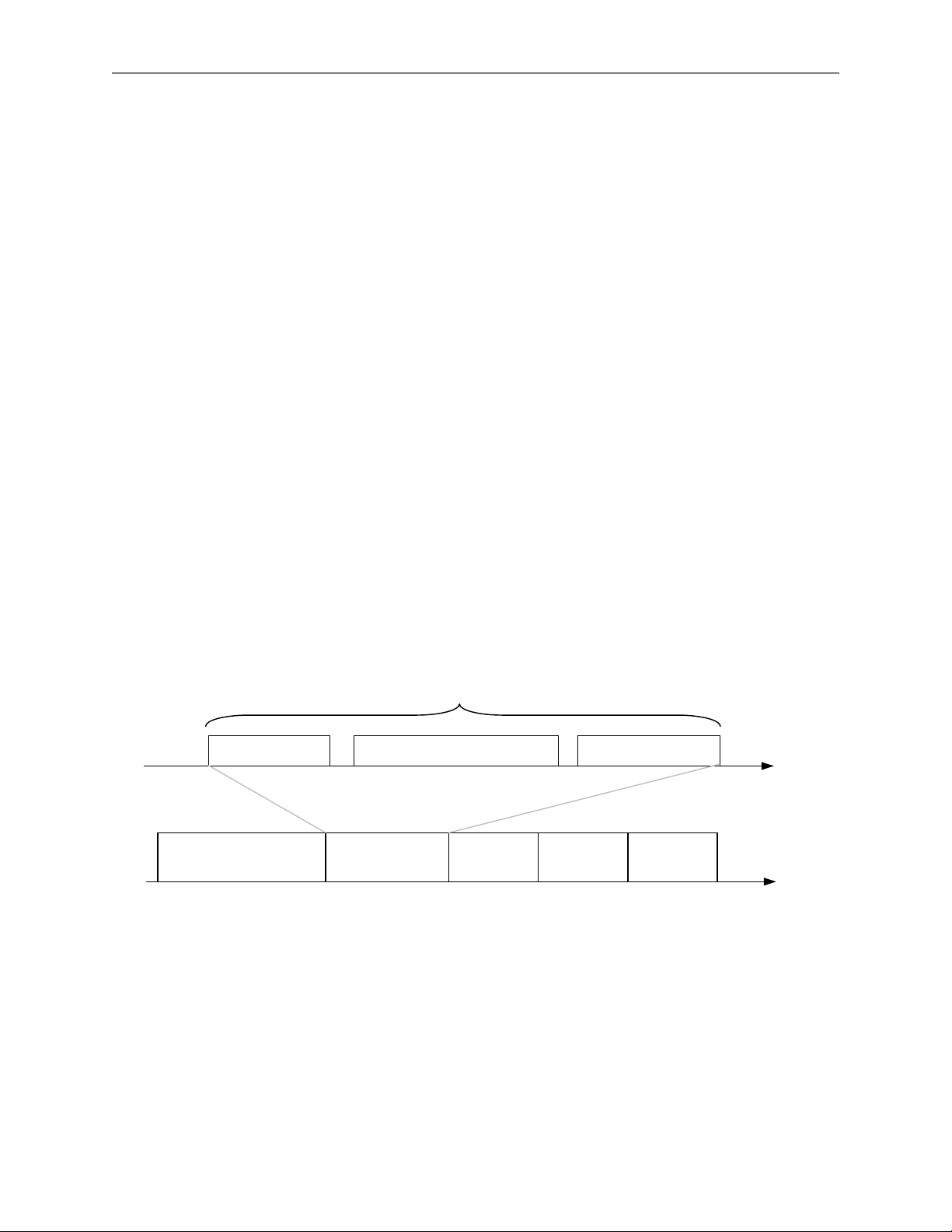
a USB transaction
Token Packet Data Packet Handshake Packet
t
XD2
ISO:IN:1023
XD3
BULK:OUT:64
XD8
SETUP
XDC
INT:IN:2
XDD
INT:IN:1
t
Fig. 3 USB transaction and UHC124 transaction batch
For instance, five transactions are grouped together to form a transaction batch (Fig. 3) with
• an isochronous, IN transaction of 1,023 bytes for real time imaging via XD
• a full speed, bulk OUT transaction of 64 bytes for a printer via XD
• a SETUP transaction sent to a low speed device via XD
• a low speed, IN interrupt transaction for a keyboard via XD
• a full speed, IN interrupt transaction for a hub via XD
;
8
; and
C
.
D
;
3
;
2
TransDimension Inc. - Proprietary
7
Page 15

TransDimension Inc. UHC124 Data Sheet
(XD)
(XD)
(XD)
(XD)
Compared with other USB host controller designs, batch processing is a very important and
unique feature of UHC124. Our software/hardware co-design solves the serious shortcomings of
other embedded USB host controller designs that generate an interrupt upon completion of every
USB transaction. These naïve designs:
• result in significant loss of USB bus bandwidth since the invocation (interrupt latency time)
and execution of the interrupt service routine (ISR), (or of certain portion of the ISR at the
minimum,) cannot overlap with USB bus activity. This problem is more obvious and
damaging when data packet sizes are small, which is typical for many USB applications,
making double buffering impractical.
• waste MCU’s time due to processor/RTOS overhead for ISR invocation and execution.
With its batch processing capability, a single register write to the UHC124 can dispatch
altogether up to 16 transactions, and a single interrupt is generated only after the completion of
all of them. The system throughput is therefore significantly improved maximizing the
bandwidth on the USB. At the same time, the number of interrupts to the MCU is greatly
reduced, saving processor resources for non-USB activities.
Before a batch is dispatched, a set of XDs must be allocated. Such a XD, designated for a
transaction, must then be specified (See Section 10). The batch is dispatched under the control
of user software (see Section 5 for details). XDs in a batch are processed by the UHC124 in
sequence - the one with the lowest index is processed first.
Multiple batches may be dispatched and processed by the UHC124 within a single USB frame (1
ms ± 0.5 µS). For easy programming, UHC124 allows transactions to spill over the USB frame
boundaries - if transactions scheduled for a batch cannot be completed in the current frame, they
will be transparently attempted following a hardware-generated Start of Frame (SOF).
A transaction batch involving XD0, XD1, XD4, and XDC
XACT
XACT
SOF
XACT
XACT
t
Fig. 4 Transactions in a batch “spill over” the boundary of a USB frame
The Host Controller Driver (HCD) may use the UhcMaxOverhead Register (see Section 5) to
limit the number of transactions in a frame to any number, giving user the flexibility of spreading
multiple transactions over several frames using a single batch.
The HCD, however, should take careful consideration of the total time required for a scheduled,
yet to be dispatched transaction batch, as well as on the real time remaining in the current frame,
if frame sensitive isochronous and interrupt transactions are present in the embedded application.
TransDimension Inc. - Proprietary
8
Page 16

TransDimension Inc. UHC124 Data Sheet
Instructions will be given in Section 10 on how to calculate time required for a single
transaction, and that for a batch of multiple transactions.
2.4 Data Memory
The 2,048 bytes of data memory (DM) built into the UHC124 serve as data buffers shared
between the MCU and USB system. Unless the data packet is known to be of zero length, a
block of DM of proper size must be allocated for the transaction. The starting address and the
length of this memory block (in bytes) must be specified in the XD.
For a SETUP or OUT transaction, data must be written into this allocated buffer area before the
transaction can be dispatched along with a batch. For an IN transaction, on the other hand, data
will become available after the transaction is completed, provided that no exceptions occurred
during transaction processing, where an exception is a device Stall, device Nak, Timeout, or data
transfer Error as defined in USB Specification [8.5:162].
2.5 Double Buffering
Double buffering, and its more general form circular buffering, are effective ways to maximize
the USB system throughput. Note that UHC124 supports dual port memory access to its entire
addressing space (control registers, CM and DM). Together with its batch processing capability,
double buffering becomes attractive even for transactions with small data packets.
XD0
XD
4
XD
XD
1
Cluster
5
Cluster
XD
XD
1
C
XD7
Fig. 5 Double buffering of two XD clusters
Depending on the application, user software may organize XDs into two or more XD clusters.
USB transactions associated with a cluster are dispatched as a batch. In Fig. 5 two XD clusters
are employed for double buffering. Note that a XD (XD1) is included in more than one cluster.
While one batch for Cluster A is being processed by the UHC124, another batch for Cluster B is
dealt by user software by which completed transactions are processed, and new ones prepared.
Once the batch for Cluster A is completed, the user software enables the batch for Cluster B.
In the presence of isochronous transfers, XD clusters must be scheduled in such a way that each
USB frame contains exactly one transaction for each active isochronous endpoint. Under the
circumstance, a XD cluster must not take longer than approximately 950 µS on the USB bus.
TransDimension Inc. - Proprietary
9
Page 17

TransDimension Inc. UHC124 Data Sheet
For UHC124, the software overhead involved to swap two operating XD clusters is minimum –
only one 16-bit register (UhcTransSelect) and an 8-bit register (UhcControl) need to be updated.
See Section 5 for descriptions on these registers.
2.6 Interrupt to MCU
Under user software control, the UHC124 may generate an interrupt (active low) to the MCU
upon any one of the following conditions and/or events:
• Root hub port status change
• Batch completion (i.e., all transactions in the batch have been processed)
• Batch stop. Software may elect to stop a batch after a transaction if:
- any one of the transactions in the batch is successfully completed;
- any one of the transactions in the batch fails (device Stall, Timeout or data/packet Error);
or
- the targeted USB device has returned a Nak for any one of the transactions in the batch
• Host controller error
• Start of frame
The first three conditions provide flexibility to balance required high data throughput and the
demand on MCU resources. All five interrupt sources can be masked.
2.7 Root Hub
The UHC124 employs a fully qualified, market proven 4-port USB hub, AT43312A by Atmel
Corp., (San Jose, CA) as its root hub. USB transceivers are built-in for all four downstream
ports. Technical details for the root hub are given in Section 7.
2.8 External Crystal/Oscillator
A PLL (Phase Locked Loop) is integrated on-chip to generate, from a single 6 MHz crystal or
crystal oscillator, the 48 MHz, 12 MHz and 6 MHz clock signals required by UHC124 internal
circuitry minimizing EMI. Section 9 gives instructions to construct a working oscillator circuit
as well as an external compensating RC network for the internal PLL.
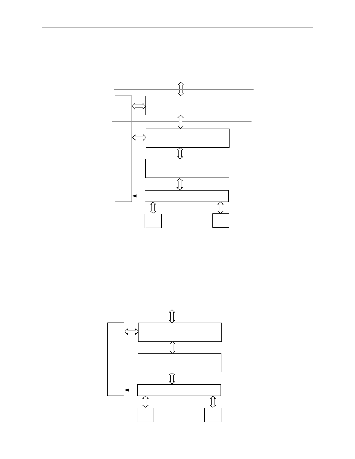
2.9 About UHCI and OHCI
UHC124 is fully compliant with USB Specification 2.0 (for full speed and low speed operation).
However, it is not UHCI/OHCI because it is not intended for the PCI bus. OEMs may develop
or license, a HCD providing a software interface that appear to the rest of the USB host stack as
if there were a UHCI or an OHCI compliant host controller.
In Fig. 6, a carefully crafted USB host engine “steals” a small fraction of the MCU’s time, to
support UHCI/OHCI operation. The UHCI support for the UHC124 is readily available from
TransDimension. Please contact sales@transdimension.com for OCHI support.
TransDimension Inc. - Proprietary
10
Page 18
TransDimension Inc. UHC124 Data Sheet
USB host software (USBD, etc)
Higher Level
HCDI
HCD for OHCI/UHCI
(UHC124 independent)
UHCI/OHCI
Simulated OHCI/UHCI
(UHC124 dependent)
USB Host Engine
UHC124 Interface
(MCU specific)
/INT
UHC124
USB Devices
…
Fig. 6 Software interface compatible to UHCI/OHCI
2.10 USB Host API
OEMs may license from TransDimension an OS-independent UHC124 Programming Interface
Library, supporting direct UHC124 operation and efficient USB host control independent of any
RTOS. This solution is attractive for embedded systems with dedicated USB devices. Note that
OEMs may have to write device drivers using functions in this library.
USB device driver(s)
(MCU independent)
USBD and HCD
USBDI:
API (specified by
TransDimension)
(MCU specific)
UHC124
USB Host Engine
UHC124 Interface
/INT
USB Devices
…
TransDimension Inc. - Proprietary
11
Page 19

TransDimension Inc. UHC124 Data Sheet
Fig. 7 Embedded USB host application written with UHC124 Programming Interface Library
2.11 RTOS Support
Many modern RTOS’ (real time operating system) are now supporting USB host operation with
their own USB host stacks. TransDimension has made the UHC124 working under several
widely used RTOS’, WinCE, VxWorks, Linux, etc., and on various hardware platforms
(X86/ISA, Arm, StrongArm, MIPs, etc.) Developers should be aware that under the situation, it
is in principle the responsibility of the chosen RTOS to provide various USB device drivers
(such as the one for HID devices).
2.12 System Suspend and Resume
Under the control of user software, the UHC124 may bring the USB system into suspend state,
as dictated by USB 1.1 specification [7.1.7.4:122]. While the oscillator for UHC124 is still
running, all USB bus activities, including SOF generation, are stopped. The system may be
brought out of the suspend state by HCD software, or by a remote wakeup [9.2.5.2: 181]
originated from a downstream USB device.
2.13 Power Saving State
Under the control of user software, the UHC124 may enter the power saving state, in which all
internal clocks are stopped, and the PLL is disabled. A small quiescent current (about 200 µA) is
consumed by the UHC124. Reactivating the system requires a master reset or a power on reset.
See Section 8.6 for details.
TransDimension Inc. - Proprietary
12
Page 20

TransDimension Inc. UHC124 Data Sheet
3. Signal Definitions
Abbreviations of signal types:
I = Input
O = Output
B = Bi-directional
V = Power supply, ground
3.1 Oscillator and PLL
Name Type Pin No. Description
OSC1 I 17 Oscillator Input: input to the inverting oscillator amplifier.
OSC2 O 18
LPF I 19
3.2 MCU Interface
Name Type Pin No. Description
A11:A0 I 13:2 Address Bus: A11(pin 13) selects CM or DM.
D7:D4
D3:D0
B
53:50
47:44
/CS I 15 Chip Select: active low.
/WR I 55 Memory Write Strobe: active low.
/RD I 56 Memory Read Strobe: active low.
MODE
I
14
Oscillator Output: output of the inverting oscillator
amplifier.
PLL Filter: connecting to a passive RC network; see Section
9 on proper usage of this pin.
Data Bus: D7 is the most significant bit.
Memory Access Mode.
MODE = 1: Non-multiplexed memory access. D
7:D0
are
connected to the MCU’s data bus, A11:A0 to its address bus;
MODE = 0: Multiplexed memory access with autoincremented address. When accessing a block of UHC124
memory, the 12-bit starting address is first latched into the
chip by writing the least significant 8-bits of the address into
D7:D0 while holding ADS high, and placing the most
significant 4-bits of the address on A
. Data is then
11:A8
retrieved out of, or stored into UHC124 memory with
successive read or write operations through D7:D0, while pin
ADS is pulled low. The memory address is automatically
incremented internally for each subsequent memory access.
A7:A0 are not used under this mode.
TransDimension Inc. - Proprietary
13
Page 21

TransDimension Inc. UHC124 Data Sheet
ADS
I
62
Address/Data Select: see discussion on signal MODE; When
MODE = 1, this pin has no effect, and it should be tied to
VSS for noise immunity.
/INT O 61 Interrupt: generated for microprocessor; active low.
/RESET I 54 Master Reset: resets entire USB system; active low.
GNDP I 63
Voltage Reference: for built-in power on reset (POR),
connect to V
(ground) for normal operation.
SS
3.3 USB Root Hub Ports
Name Type Pin No. Description
DP1
DP
2
DP3
DP4
DM1
DM2
DM3
DM4
/OC1
/OC2
/OC3
/OC4
/PO1
/PO2
/PO3
/PO4
B
B
I
O
34
37
39
41
35
Port Data for USB I/O:
DP1:DP4 and DM1:DM4 are the differential signal pairs to
connect downstream USB devices [7.1:107].
38
40
42
25
26
27
28
29
30
31
32
Over Current Indicator: input signal to indicate to the root
hub that over current is detected at the port; active low. If
/OCn is asserted, the root hub will de-assert /POn, and report
the status in the root hub’s port status register.
Power On Switch: output signal to turn on the external
voltage supplying power to a port; active low. /POn is deasserted when a power supply problem is detected at /OCn,
where n is 1, 2, 3, or 4.
3.4 Test Modes
Name Type Pin No. Description
TMS3:
TMS0
TEST4:
TEST
0
I 60:57
B
43,
24:21
Test Mode Select: used only for factory testing; connect to
VSS for normal operation.
Test Signal I/O: used only for factory testing; working in
output mode during normal operation, they must be left
floating.
3.5 Power and Ground
Name Type Pin No. Description
VDD V
VSS V
1,20
33,48
16,36
49, 64
3.3V Power Supply. All four pins must be connected.
Ground. All four pins must be connected.
TransDimension Inc. - Proprietary
14
Page 22

TransDimension Inc. UHC124 Data Sheet
4. Memory Map
The UHC124’s control memory (CM), data memory (DM), and its registers are organized into a
4 kB block, which, at the developer’s discretion, may be mapped into a MCU’s memory space.
000H
00FH
010H
3FFH
400H
4FFH
500H
6FFH
700H
7FFH
800H
FFFH
Fig. 8 UHC124 memory map (memory block sizes not to scale)
Reading from a location in a reserved segment of UHC124 addressing space returns 00H, while
writing to such a location has no effect.
Note that the MCU and UHC124’s control circuitry share the entire addressing space of the
UHC124. An arbitration mechanism inside the chip allows dual port access.
The lowest 16 bytes of this addressing space are system control/status registers described in
detail in the next section.
Control Registers (16 bytes)
Reserved
Control Memory (CM, 256 bytes) for
16 Transaction Descriptors (XDs),
each of which is 16 bytes.
Reserved
Magic Reset (used only for factory
test).
Data Memory (DM, 2048 bytes)
TransDimension Inc. - Proprietary
15
Page 23

TransDimension Inc. UHC124 Data Sheet
5. Control Registers
5.1 Overview
This section discusses UHC124 control registers:
• UhcControl 000-001H system level control
• UhcTransSelect 002-003H batch transaction select
• UhcTransDone 004-005H transaction status check
• UhcIntpStatus 006H interrupt status report
• UhcIntpEnable 007H interrupt enable/disable
• UhcFmInterval 008-009H frame interval
• UhcFmRemaining 00A-00BH frame remaining
• UhcFmNumber 00C-00DH frame number
• UhcMaxOverhead 00EH maximum frame overhead
• UhcMagicNumber 00FH chip/version id, port status change
5.2 UhcControl Register
This register defines the operating states of the UHC124, and is used by the HCD to issue
commands such as to initiate a soft reset, to dispatch a transaction batch, and to bring the
UHC124 from one host controller functional state (HCFS) to another.
Setting (writing a ‘1’ to) a specific bit of the UhcControl register is a command to the UHC124,
whereas writing a 0 to that bit has no effect. A total of seven commands can be applied to the
UHC124 through this register:
• PowerSave write ‘1’ to Bit 7 enter power save state
• SoftReset write ‘1’ to Bit 5 soft reset
• USBReset write ‘1’ to Bit 4 USB system reset
• USBSuspend write ‘1’ to Bit 3 enter suspend state
• USBResume write ‘1’ to Bit 2 resume from suspend state
• USBOperational write ‘1’ to Bit 1 enter operational state
• BatchOn write ‘1’ to Bit 0 dispatch a transaction batch
Writing to register UhcControl (000H) with multiple bits set to ‘1’, (such as 06H whose bit
pattern contains two 1’s,) introduces ambiguity and/or inconsistency into the system, and is
therefore ignored by the UHC124.
Moreover, only a valid command under the current HCFS is accepted by the UHC124. For
instance, command USBResume does not make sense unless the USB system is currently
suspended. See Section 8 on HCFS definitions and valid state transitions.
TransDimension Inc. - Proprietary
16
Page 24

TransDimension Inc. UHC124 Data Sheet
Developers should be aware that since the clocks for the MCU are in general not synchronized
with that of UHC124’s, a command takes up to 167 ns to become effective.
Reading the register retrieves the UHC124’s current HCFS:
OWERSAVE Bit 7 Power saving state (always read 0)
• P
• U
SBRESET Bit 4 USB system reset in progress
• USBSUSPEND Bit 3 system in suspend state
• USBRESUME Bit 2 system is resuming from suspend state
• USBOPERATIONAL Bit 1 system in normal operation state
• BATCHON Bit 0 a batch is being processed by UHC124
In the following, a word containing letters of mixed upper and lower cases, such as
USBSuspend, is a command issued to UHC124 (by writing a ‘1’ to some bit of UhcControl).
The very same word in upper case (small caps), such as USBSUSPEND, is the corresponding
HCFS that the system currently assumes, which is obtained by reading the UhcControl register.
In addition, HC denotes the Host Controller (UHC124), and HCD stands for Host Control
Driver, which is used interchangeably with phase “user software”.
Register Address: 000H (low byte)
001H (high byte)
Reset: Signals vary (see bit descriptions below)
Read/Write
Bit Default
HCD HC
Description
15:8 00H Reserved
7
0
R/W
R/W
PowerSave/ POWERSAVE:
When a ‘1’ is written into this bit, the UHC124 enters
OWERSAVE state immediately if the current state is
P
USBSUSPEND (see section 8.6 for more detailed steps).
The UHC124’s internal clocks are all stopped in
POWERSAVE state.
To exit the POWERSAVE state (i.e., to have the bit cleared),
MasterReset (/RESET) must be applied which restarts
clocks, and places the UHC124 in U
SBRESET state.
Since it is impossible to access memory or registers in the
POWERSAVE state, this bit is always 0 when read.
6 0 Reserved.
TransDimension Inc. - Proprietary
17
Page 25

TransDimension Inc. UHC124 Data Sheet
5
0
W
SoftReset:
This bit is set by the HCD to initiate a software reset, which
brings the UHC124 into U
initializes all UHC124 registers and state machines - except
UhcFmInterval, UhcFmNumber, UhcFmRemaining and
UhcMaxOverhead. A batch in progress will be aborted.
R
SBSUSPEND state. SoftReset
Unlike USBReset (Bit 4), SoftReset takes less than 200 ns
to accomplish, and it does not reset the root hub and all
downstream ports.
This bit is always 0 when read.
4
1
R/W
R/W
USBReset/USBRESET:
Setting this bit to 1 initializes all UHC124 registers, state
machines, the root hub and all downstream ports, regardless
of the UHC124’s current HCFS. The HCD must ensure that
the UHC124 remains in USBRESET state for a minimum of
50 ms per USB Specification 1.1 [10.2.8.1:214].
PowerOnReset (generated internally by the UHC124 when
power is applied to it the first time) and MasterReset
(/RESET pin) have almost the same effect as that of
USBReset, except that for PowerOnReset and MasterReset,
memory access is disabled during the first 12 ms.
This bit is cleared upon user issuing a SoftReset command,
or a USBOperational command.
TransDimension Inc. - Proprietary
18
Page 26

TransDimension Inc. UHC124 Data Sheet
3
0
R/W
R/W
USBSuspend/USBSUSPEND:
Setting this bit to ‘1’ while the UHC124 is in
SBOPERATIONAL state brings it to USBSUSPEND state,
U
which disables batch dispatching and SOF generation. This
in turn, in less than 5 ms, makes the root hub and connected
devices to enter their respective suspend state [7.1.7.4:122].
If there is a batch in progress, U
SBSUSPEND will be entered
after its completion.
Another way to bring UHC124 into USBSUSPEND state is
through SoftReset.
The UH124C is brought out of USBSUSPEND (to enter
USBRESUME) upon a RemoteWakeup originated by a
downstream USB device, or by the HCD issuing a
USBResume command.
It is also possible to exit from USBSUSPEND, and enter
USBOPERATIONAL directly by writing a ‘1’ into Bit 1 of the
UhcControl register. This method is effective when The
UHC124 remains in USBSUSPEND state for less than 3 ms,
and none of the devices, including the root hub, have yet
actually been suspended. A typical use of this feature is to
resume normal USB operation immediately following a
SoftReset.
This bit is cleared upon PowerOnReset, MasterReset, and
USBReset. It is set after SoftReset.
2
0
R/W
R/W
USBResume/USBRESUME:
When set to ‘1’ while the system is in USBSUSPEND, the
UHC124 enters U
SBRESUME state, in which batch
dispatching and SOF generation are still being disabled.
A RemoteWakeup from a downstream device while the
system is in USBSUSPEND will also cause the UHC124 to
enter USBRESUME automatically.
The system remains in U
SBRESUME state for about 20 ms
before it automatically falls into USBOPERATIONAL.
This bit is cleared upon PowerOnReset, MasterReset,
USBReset, and SoftReset.
TransDimension Inc. - Proprietary
19
Page 27

TransDimension Inc. UHC124 Data Sheet
1
0
R/W
R/W
USBOperational/USBOPERATIONAL:
Setting this bit to ‘1’ while the UHC124 is in USBRESET or
SBSUSPEND enters state USBOPERATIONAL, which enables
U
SOF generation and batch dispatching.
The user software may notice that the first batch dispatched
after entering U
SBOPERATIONAL may take longer time to
complete. This is because transactions in a batch cannot be
processed by the UHC124 until the first SOF is generated,
which may take up to 1 ms to occur.
Caution must be taken when USBOPERATIONAL is entered
directly from USBSUSPEND – it is possible that the system
has been in that state for longer than 3 ms, and some or all
of its connected devices have already entered their
respective suspend state. A transaction aimed to such a
(suspended) device will inevitably result in a transaction
TimeOut. This problem can be resolved automatically with
USB’s error recovery protocol [8.7:172].
This bit is cleared upon PowerOnReset, MasterReset,
USBReset, and SoftReset.
0
0
R/W
R/W
BatchOn/BATCHON:
Setting this bit to ‘1’ while the system is in
USBOPERATIONAL dispatches a transaction batch. It is reset
to 0 if any one of the following condition occurs:
1. All selected transactions have been processed;
2. A stop condition for a transaction, as specified in its XD,
is satisfied (see Bits StopOnSucc, StopOnNak, and
StopOnFail of XDControl in the next section).
3. Batch is aborted due to MasterReset, USBReset or
SoftReset.
This bit is cleared upon PowerOnReset, MasterReset,
USBReset, and SoftReset.
5.3 UhcTransSelect Register
Register Address: 002H (low byte)
003H (high byte)
Reset: PowerOnReset, MasterReset, USBReset and SoftReset.
TransDimension Inc. - Proprietary
20
Page 28

TransDimension Inc. UHC124 Data Sheet
This register is used to select a subset of transactions, out of 16 XDs in CM, to form a transaction
batch. XDn, located at 4n0H – 4nFH of the UHC124’s addressing space, is included in the batch
if Bit n of UhcTransSelect is set to ‘1’, where n = 0, 1, …, 9, A, …, E, F, in hex.
Note that once dispatched, transactions selected in a batch are processed by the UHC124, one at
a time, starting from the XD with the lowest index.
5.4 UhcTransDone Register
Register Address: 004H (low byte)
005H (high byte)
Reset: PowerOnReset, MasterReset, USBReset and SoftReset.
This register is used to monitor the progress of a transaction batch. If Bit n of UhcTransDone is
set by the UHC124, it indicates that the transaction associated with XDn has been processed.
UhcTransDone is cleared by the UHC124 as soon as a BatchOn command is issued to the
UhcControl register.
Upon completion or termination of a batch, Bit 0 of UhcControl is set back to ‘0’, the status of a
transaction involved in this batch, as far as its progressing status is concerned, can be derived
from information provided in UhcTransSelect and UhcTransDone:
Bit n of
UhcTransSelect
0 0
1
Bit n of
UhcTransDone
1
Transaction Status
Transaction associated with XDn was not
selected for the batch.
Transaction associated with XDn was selected
for the batch, and has been processed by the
UHC124. Status of the transaction is in
XDStatus of XDn. (See next section for
detailed discussion of XDs).
1
0
Two possibilities: (i) transaction associated
with XDn was selected for the batch, but has
not been processed; (ii) The batch stopped in
response to an anticipated outcome of an
earlier transaction. See description on XD
(next section) for details on batch stop
conditions.
0 1 System error (not suppose to happen).
5.5 UhcIntpStatus Register
Register Address: 006H
Reset: PowerOnReset, MasterReset, USBReset, and SoftReset.
TransDimension Inc. - Proprietary
21
Page 29

TransDimension Inc. UHC124 Data Sheet
This register reports the following system events and conditions that may cause an interrupt on
the /INT pin:
• BatchStopped Bit 7 batch stopped before all transactions are processed
• BatchCompleted Bit 6 all transactions in a batch have been processed
• HostError Bit 3 a host error occurred
• ResumeDetected Bit 2 entering U
SBRESUME state
• PortChange Bit 1 status change occurred on one of the root hub ports
• StartOf Frame Bit 0 start of a USB frame
A bit is asserted (set to ‘1’) as soon as the designated event occurs, or condition holds. User
software may acknowledge the event by writing a ‘1’ to the bit, which will have the bit cleared.
All bits will remain ‘1’ after asserted, and be cleared explicitly by user software (writing ‘1’ to
them). In addition, Bit 7 (BatchStopped) and Bit 6 (BatchCompleted) will also be automatically
cleared by UHC124 upon a BatchOn command applied to the UhcControl register.
Read/Write
Bit Default
7
0
HCD HC
R/W
W
BatchStopped:
This bit is set when a batch is stopped due to a software
anticipated stop condition that occurred as the result of a
transaction (Success, Nak, or Failure). See description on
Description
XDControl in the next section for details.
The UHC124 clears this bit automatically upon dispatching
of a new transaction batch.
6
0
R/W
W
BatchCompleted:
This bit is set when all selected XDs in a batch have been
processed.
The UHC124 clears this bit automatically upon dispatch of a
new transaction batch.
5:4 00 Reserved.
3
0
R/W
W
HostError:
This bit is set when the UHC124 detects a host controller
error – often caused by a transaction with an illegal data
packet that would take more than 1 ms to complete.
TransDimension Inc. - Proprietary
22
Page 30

TransDimension Inc. UHC124 Data Sheet
2
0
R/W
W
ResumeDetected:
This bit is set when the UHC124 enters USBRESUME state
(from U
SBSUSPEND) in response to a USBResume
command, or to a RemoteWakeup originated from a
downstream USB device.
1
0
R/W
W
PortChange:
This bit is set whenever there is a status change in the root
hub, or in any of its four downstream ports.
It is the responsibility of user software to identify the port
(or root hub itself) that has had the change (see description
on MagicNumber register), and to find out what happened.
The latter requires issuing of a hub class request to retrieve
the status of that port (or of the root hub).
0
0
R/W
W
StartOfFrame:
This bit is set by the UHC124 at the beginning of each USB
frame. The actual SOF packet is generated approximately
12 FSBT (approximately 1 µs) after the bit is asserted.
5.6 UhcIntpEnable Register
Register Address: 007H
Reset: PowerOnReset, MasterReset, USBReset, and SoftReset.
Bits in UhcIntpEnable have a one-to-one correspondence with those in UhcIntpStatus. A level
triggered interrupt is generated (pin /INT is pulled low) when any one of designated
events/conditions is reported by UIntpStatus, and the corresponding interrupt source is enabled
in UhcIntpEnable.
Setting ‘1’ to a bit of this register enables the corresponding interrupt source.
TransDimension Inc. - Proprietary
23
Page 31

TransDimension Inc. UHC124 Data Sheet
Read/Write
Bit Default
HCD HC
Description
7 0 R/W R BatchStopped Interrupt Enable.
6 0 R/W R BatchCompleted Interrupt Enable.
5:4 00 Reserved.
3 0 R/W R HostError Interrupt Enable.
2 0 R/W R ResumeDetect Interrupt Enable.
1 0 R/W R PortChange Interrupt Enable.
0 0 R/W R StartOfFrame Interrupt Enable.
5.7 UhcFmInterval Register
Register Address: Low byte: 008H
High byte: 009H
Reset: PowerOnReset, MasterReset, and USBReset.
The least significant 14 bits of the UhcFmInterval register determine the duration of a USB
frame in terms of its full speed (12 Mbit per second) bit times (FSBTs). This register can be used
to fine-tune the frame duration for certain applications.
Note that USB specification requires that the frame to be 1 ms ± 0.5 µs [7.1.12:126], which
translates to 12,000 ± 6 counts for the 12 MHz clock. Setting this register to a value out of this
range may cause compatibility problems for most USB devices, especially hubs. Moreover, user
software may not change the frame internal more than 1 FSBT during less than 6 frames. To
read/write from/to this register, user software must first read/write its LSB (008H), followed by
another read/write of its MSB (009H).
Read/Write
Bit Default
HCD HC
Description
15:14 Reserved
13:0
2EDFH
R/W
FrameInterval:
The register should be set to a value that is 1 less than the
number of FSBTs constituting the desired USB frame.
After a PowerOnReset, a MasterReset (/RESET pin) or a
R
USBReset, the register is default to 2EDFH (11,999 in
decimal), corresponding to a USB frame of 12,000
FSBTs, or exactly 1 ms.
If the register is updated by user software, the new value
will not take effect until the start of the next frame.
TransDimension Inc. - Proprietary
24
Page 32

TransDimension Inc. UHC124 Data Sheet
5.8 UhcFmRemaining Register
Register Address: 00AH (low byte)
00BH (high byte)
Reset: PowerOnReset, MasterReset, and USBReset.
This register is a 14-bit down counter, whose value can be read “on the fly” by user software to
determine the instantaneous time relative to the beginning of the current USB frame.
To read from this register, user software must first issue a read to its LSB (00AH), followed by
another one for the MSB (00BH).
Read/Write
Bit Default
HCD HC
Description
15:14 00 Reserved
13:0
000H
R
R/W
FrameRemaining:
The value of this register decrements once per full speed
bit time. It is reloaded with the value of UhcFmInterval
once it reaches 0. The frame boundary is the bit boundary
on which the value of this register changes from ‘0’ to that
of UhcFmInterval.
5.9 UhcFmNumber Register
Register Address: 00CH (low byte)
00DH (high byte)
Reset: PowerOnReset, MasterReset, and USBReset.
This register is an 11-bit counter, whose value is broadcast over the USB system riding SOF
packets.
While reading this register, the HCD must read the low byte (00CH) first.
Read/Write
Bit Default
HCD HC
Description
15:11 00000 Reserved.
10: 0
000H
R
R/W
FrameNumber:
The register is incremented by 1 at each frame boundary,
following which a SOF packet carrying the current frame
number is generated.
TransDimension Inc. - Proprietary
25
Page 33

TransDimension Inc. UHC124 Data Sheet
5.10 UhcMaxOverhead Register
Register Address: 00EH
Reset: PowerOnReset, MasterReset, and USBReset.
This register is used to fine-tune the time usable for USB transactions in a frame. As illustrated
in Fig. 9, USB transactions can only be carried out in a frame after the SOF packet, and before
EOF
. The value of UhcMaxOverhead ranges from 10 to 255. Setting the register to a value less
M
than 10 is not recommended.
Before a transaction is processed by the UHC124, user software may wish to estimate the time
required for the transactions to be successfully carried out, or timeout, before EOF
in the
M
current frame. If there is not enough time, some transactions will “spill over” to the next frame.
In other words, it will not be processed until after the next SOF packet.
12
SOF
~ 35
usable for
transactions
EOF
Max
Overhead
USB Frame (12,000 bit time: 1 ms)
EOF
35
t
in full speed
bit time (FSBT)
1 FSBT = 83.3 ns
Fig. 9 USB frame under UHC124 (time not to scale)
Read/Write
Bit Default
HCD HC
MaxOverhead:
Description
7: 0
C0H R/W
R
Number of USB Full Speed Bit Times (FSBTs) between
EOFM and EOF1 (10-255 decimal). See Fig. 9.
5.11 UhcMagicNumber Register
Register Address: 00FH
Reset: PowerOnReset, MasterReset, USBReset, and SoftReset.
This register is used to read the UHC124’s chip identification (DBH), as well as to retrieve
PortChange, i.e., which down stream port, or the root hub itself, has a status change. Operation
of UhcMagicNumber register is illustrated with the following state diagram:
TransDimension Inc. - Proprietary
26
Page 34

TransDimension Inc. UHC124 Data Sheet
)
)
RD (chip id) or
WR (not 55H)
RD [chip id] or
WR (not AAH)
WR (55H
WR (AAH
RD [port/hub status change] or
WR (anything)
Fig. 10 Operation of UhcMagicNumber register (00FH)
The following steps must be followed to read PortChange:
1. Read the register;
2. Write 55H to the register;
3. Write AAH to the register; and finally
4. Read the register - retrieving a byte containing PortStatusChange and HubStatusChange:
Read/Write
Bit Default
HCD HC
Description
7:5 000 Reserved.
PortStatusChange:
4:1
0000
R
W
Bit n is asserted if there has been a status change on Port n
of the root hub.
0
0
R
W
HubStatusChange:
Asserted if there has been a status change on the root hub.
Note that this byte reflecting port/hub status change is identical to that obtained through an IN
transaction via EP1, an IN interrupt endpoint, of the root hub [11.13.1:257]. An asserted status
change bit can be cleared only through a ClearPortFeature request as described in the USB
specification [11.13.2:257].
TransDimension Inc. - Proprietary
27
Page 35

TransDimension Inc. UHC124 Data Sheet
6. Transaction Descriptor
6.1 Overview
The 256 bytes of UHC124’s addressing space starting from 400H are reserved as Control
Memory (CM), which holds 16 transaction descriptors (XD) denoted as XD
XD
, …, XDF.
A
XD Location
XD0 400H - 40FH
XD1 410H - 41FH
XD2 420H - 42FH
XD3 430H - 43FH
XD4 440H - 44FH
XD5 450H - 45FH
XD6 460H - 46FH
XD7 470H - 47FH
XD8 480H - 48FH
XD9 490H - 49FH
XDA 4A0H - 4AFH
XDB 4B0H - 4BFH
XDC 4C0H - 4CFH
XDD 4D0H - 4DFH
XDE 4E0H - 4EFH
XDF 4F0H - 4FFH
Each XD consists of the following fields:
XDControl 1 byte @ offset 0 transaction control
XDStatus 1 byte @ offset 1 transaction status
XDDevAddress 1 byte @ offset 2 device address (0-127)
XDEndpoint 1 byte @ offset 3 endpoint number (0-15)
XDBufAddress 2 bytes @ offset 4 address of data area (800-FFFH)
XDBufLength 2 bytes @ offset 6 data length (0-1,023)
XDXferCount 2 bytes @ offset 8 number of bytes not transferred
Upon a BatchOn command, the XDs selected for the batch are loaded, one at a time, into the
chip’s USB Host Control Logic (Fig. 1), and processed. As long as the BATCHON bit of
UhcControl is set, the user software should not attempt to modify any selected, yet to be
processed XDs. See discussion on registers UhcTransSelect and UhcTransDone in the previous
section for details.
, XD1, XD2, …XD9,
0
TransDimension Inc. - Proprietary
28
Page 36

TransDimension Inc. UHC124 Data Sheet
6.2 XDControl
XD Offset: 0
XDControl contains information needed to process the transaction. It must be specified before
the transaction is dispatched along with a batch.
Bit Description
7
StopOnSucc:
When this bit is set, the current batch stops after the transaction of this
XD if the transaction has been successful.
For IN, this means that the device returns a data packet to the host with
no error. For SETUP and non-isochronous OUT, this means that the host
received an ACK from the device. For isochronous OUT, the transaction
is always considered successful after it is dispatched.
If the batch must be continued after this transaction, regardless of its
outcome, set Bits 7:5 to 000.
6
StopOnNak:
When this bit is set, the current batch stops after the transaction of this
XD if device has responded with a Nak.
5
StopOnFail:
When this bit is set, the current batch stops after the transaction
associated with this XD when one of following occurs:
• device has returned Stall;
• device has failed to respond within 18 bit times (Timeout); or
• there has been an Error in the packet returned by the device.
4
DevSpeed:
Data rate for the targeted device – 0: full speed (12 Mbits/sec); 1: low
speed (1.5 Mbits/sec).
3
Isochronous:
This bit is set to ‘1’ if the transaction is isochronous.
2
OutDataSeq:
Data sequence toggle for a non-isochronous, OUT transaction - 0:
DATA0; 1: DATA1 [8.6:168].
This bit is irrelevant for IN transactions. For SETUP or isochronous
OUT transactions, this bit should be set to ‘0’.
TransDimension Inc. - Proprietary
29
Page 37

TransDimension Inc. UHC124 Data Sheet
1:0
TransType:
Type of the transaction – 00: SETUP (host to device); 01: OUT (host to
device); 10: IN (device to host); and 11: reserved.
6.3 XDStatus
XD Offset: 1
The UHC124 returns the status of the transaction in this location of the XD after the transaction
is completed. User software may read this byte upon completion of the batch when B
ATCHON of
UhcControl is no longer asserted, or at the minimum, after this transaction is processed (To
determine whether a transaction in a batch has been processed, registers UhcTransSelect and
UhcTransDone must be consulted, see previous section for details.)
Bit Description
7 Reserved.
6
Stall:
This bit is asserted by the UHC124 as the result of a Stall packet received
from the endpoint of the USB device.
5
Error:
The bit is asserted by the UHC124 if during the transaction
• a CRC error occurred for the data packet of an IN transaction;
• a PID error occurred; or
• a corrupted packet (such as missed bit stuffing bits) is encountered.
4
Overflow:
This bit is set when the UHC124 receives more data from the device than
that specified in XDBufLength. Note that excessive data is truncated.
This bit is irrelevant for SETUP and OUT transactions.
3
Timeout:
This bit is set by the UHC124 as it fails to receive any response from the
device 18 bit times after the token packet in an IN transaction, or after
the device bounded data packet in a SETUP or OUT transaction.
2
Nak:
The bit is set if the UHC124 has received a Nak packet from the device
for this transaction.
TransDimension Inc. - Proprietary
30
Page 38

TransDimension Inc. UHC124 Data Sheet
1
InDataSeq:
This bit is set by the UHC124 for an IN transaction - 0: a DATA0 data
packet has been received; 1: a DATA1 data packet has been received.
It is irrelevant for OUT transactions.
0
Ack:
This bit is asserted if the UHC124 has received an Ack packet from the
device for a SETUP transaction, or a non-isochronous OUT transaction.
It is irrelevant for IN transactions and isochronous OUT transactions.
6.4 XDDevAddress
XD Offset: 2
Bit Description
7 Reserved.
6:0
DevAddress:
This is the 7-bit address of the USB device targeted by the transaction.
6.5 XDEndpoint
XD Offset: 3
Bit Description
7:4 Reserved.
3:0
Endpoint:
This is the 4-bit endpoint number of the USB device targeted by the
transaction.
TransDimension Inc. - Proprietary
31
Page 39

TransDimension Inc. UHC124 Data Sheet
6.6 XDBufAddress
XD Offset: 4 (low byte)
5 (high byte)
Bit Description
15:12 Reserved.
11:0
BufAddress:
This is the starting address of the data area allocated for the transaction.
The 12-bit address specified here is relative to 000H. (Thus a valid value
for the field must fall between 800H and FFFH.)
6.7 XDBufLength
XD Offset: 6 (low byte)
7 (high byte)
Bit Description
15:10 Reserved.
9:0
BufLength:
This is the length of the data (in bytes) for the transaction.
Note that for an IN transaction, the data packet may contain more data
than anticipated. In this case, the Overflow bit of XDStatus is asserted,
and the excessive data bytes are truncated. It is therefore recommended
to always employ here the size of the endpoint buffer for IN transactions,
even if it may not be completely filled.
For EP0, the size of the endpoint buffer is given in field
bMaxPacketSize0 of the device descriptor [9.6.1:196]; and for other
endpoints, it is presented to the host in field wMaxPacketSize of the
corresponding endpoint descriptor [9.6.4:203].
TransDimension Inc. - Proprietary
32
Page 40

TransDimension Inc. UHC124 Data Sheet
6.8 XDXferCount
XD Offset: 8 (low byte)
9 (high byte)
Bit Description
15:10 Reserved
9:0
XferCount:
This contains the result of a down counter in the USB Host Controller
Logic (Fig. 1). At the beginning of the transaction, the counter was
loaded with the value of XDBufLength. The counter is then decremented
by one for every byte transferred. If more bytes than that indicated by
BufLength are actually transferred, XferCount is set to zero, and the
Overflow bit in XDStatus is asserted.
The content of this down counter is copied to XferCount only after the
transaction is completed. Thus it may not be read “on the fly” while the
transaction is in progress. Moreover, XferCount is meaningful only for
IN transactions – it is always zero for SETUP and OUT transactions.
TransDimension Inc. - Proprietary
33
Page 41

TransDimension Inc. UHC124 Data Sheet
7. Root Hub
The UHC124 employs the AT43312A (by Atmel) as its root hub. It supports the following
standard descriptors: Device Descriptor, Configuration Descriptor, Interface Descriptor,
Endpoint Descriptor, and Hub Descriptor. Other supported standard requests and hub class
requests include ClearHubFeature, ClearPortFeature, GetBusState, GetHubDescriptor,
GetHubStatus, GetPortStatus, SetHubDescriptor, SetHubFeature, SetPortFeature. See USB
Specification 1.1 [11.16:266] for details.
7.1 Down Stream Ports
Each of the four downstream ports of the root hub can be connected to a full speed or a low
speed device. 15 kΩ pull-down resistors are required at DPn and DMn data lines (n = 1, 2, 3, or
4). To satisfy the impedance matching requirement, a 22 Ω resistor must be inserted between a
USB data line (DPn or DMn) and its corresponding pin at the Type A connector. See Fig. 13 in
Section 9 for a schematic description.
Per USB specification, the speed of the USB device attached to a downstream port is determined
at the time of enumeration, depending on which data line (DPn or DMn) is pulled high
[7.1.5:113].
If a port is connected to a low speed device, the root hub will not propagate any traffic to that
port unless it is prefixed with a preamble PID. However, low speed packets (following the
preamble PID) are propagated down stream to both low and full speed devices. A packet targeted
to a low speed device is placed on the bus four FSBT after the preamble PID [11.8.4:252].
7.2 Port Power Management
Over-current conditions can be detected on a per port basis, and be furnished to the UHC124’s
root hub through its /OCn pins (active low, n = 1, 2, 3 or 4). As soon as /OCn is asserted, the root
hub sets the PORT_OVER_CURRENT bit of the port’s status word and the
C_PORT_OVER_CURRENT bit of the port’s status change word [11.16.2.6:273], and at the
same time, the power to the offending port is turned off.
An external switching device is needed to perform the actual “turn-on” and “turn-off” (of the
power) for each port. Any type of switching device is acceptable as long as it has a sufficiently
low voltage drop even when the device connecting to the port absorbs full power. In its simplest
form, this switch can be a P-channel MOSFET, though power-switching ICs specially designed
for USB, such as TPS2044/2054 by TI and MIC2524/2527 by Micrel are recommended.
The USB specification requires that the voltage drop at the power switch and board traces be no
more than 100 mV. A good conservative maximum drop at the power switch itself should be no
more than 75mV. Careful design and selection of the power switch and PCB layout is required to
meet the specifications.
TransDimension Inc. - Proprietary
34
Page 42

TransDimension Inc. UHC124 Data Sheet
Each port has its own power control pin /POn (active low, n = 1, 2, 3 or 4), which is asserted only
when a SetPortFeature request with feature PORT_POWER is issued to the specific port. /POn is
de-asserted upon anyone of the following conditions:
1. PowerOnReset, MasterReset or USBReset;
2. Over current condition; or
3. Request of ClearPortFeature with feature PORT_POWER.
7.3 Root Hub as a USB Device
As a special case of a USB device, the UHC124 root hub has two endpoints: Endpoint 0 (EP0),
and Endpoint 1 (EP1). EP0 is used for root hub enumeration, for port manipulation, and for
retrieving information about its configuration and hub/port status. By definition, all transfers
to/from EP0 are control transfers, more specifically, standard USB requests and hub class
requests. EP1, is an interrupt IN endpoint for reporting hub/port status change, which is to be
polled by user software every 255 ms.
Like any other USB device, the root hub must be enumerated before it can be used, which
involves, at the minimum, the following two steps:
1. Set address.
Since the root hub is always the first USB device in the system, device address 01H is
conventionally reserved for it, although for the UHC124, any address between 1-127 is also
valid.
This step is done through standard USB request SET_ADDRESS via default address 00H
[9.4.6:192].
2. Set configuration.
The root hub of the UHC124 has only one configuration (configuration number 1). User
software must explicitly set the configuration of the root hub to 1 before any hub class
requests are issued.
This step is accomplished through standard USB request SET_CONFIGURATION via the
device address assigned in the previous step (most likely, 01H) [9.4.7:193].
It is a good practice to verify, after this step, the effectiveness of the newly assigned device
address and configuration setting. This is done through standard USB request
GET_CONFIGURATION using the address assigned in Step 1 [9.4.2:189].
Device descriptor, configuration descriptors, and endpoint descriptors for a USB device carry
detailed information for its identification, characterization, and usage. Their pre-defined
contents for the UHC124 root hub are given below. They are presented only for reference
purposes - it is not necessary to have them retrieved in a user application.
TransDimension Inc. - Proprietary
35
Page 43

TransDimension Inc. UHC124 Data Sheet
The device description for UHC124’s root hub can be obtained using standard USB request
GET_DESCRIPTOR with DEVICE as its descriptor type, using DEV1 as the device address. If
the device has yet to be assigned an address, it responses to DEV0 (device address 0) [9.6.1:196].
Device Descriptor
Field Offset Size
UHC124
Root Hub
Remark
bLength 0 1 12H total length - 18 bytes.
bDescriptorType 1 1 01H DEVICE (1).
bcdUSB 2 2 0110H USB ver (1.10).
bDeviceClass 4 1 09H not used.
bDeviceSubClass 5 1 00H not used.
bDeviceProtocol 6 1 00H not used.
bMaxPacketSize0 7 1 08H EP0 max packet size (8).
idVendor 8 2 03EBH hub vendor
idProduct 10 2 3312H part id (3312).
bcdDevice 12 2 0300H version id (3.00).
iManufacture 14 1 00H not used.
iProduct 15 1 00H not used.
iSerialNumber 16 1 00H not used.
bNumConfigurations 17 1 01H single configuration.
Per USB specification, standard request GET_DESCRIPTOR with CONFIGURATION as the
descriptor type and a configuration index retrieves not only a configuration descriptor of the
device, but also interface descriptor(s), endpoint descriptor(s), as well as other class descriptors
under the configuration [9.6.2:199]. Specifically, the UHC124 root hub returns, upon this
request, a total of 25 bytes containing a configuration descriptor [9.6.2:199], an interface
descriptor [9.6.3:201], and a single endpoint descriptor [9.6.4:203].
In the following, the “m:n” notation is used in column Offset, where m gives the location of data
relative to the beginning of its specific descriptor , and n is that relative to the beginning of the
25 bytes returned by the UHC124 upon the request.
Configuration Descriptor
Field
Offset
(m:n)
Size
UHC124
Root Hub
Remark
bLength 0:0 1 09H length of conf. desc. (9).
bDescriptorType 1:1 1 02H CONFIGURATION (2).
wTotalLength 2:2 2 0019H total bytes returned (25).
bNumInterfaces 4:4 1 01H number of interfaces (1).
bConfigurationValue 5:5 1 01H the only configuration (1).
iConfiguration 6:6 1 00H not used.
bmAttributes 7:7 1 E0H self pwr., remote wakeup.
bMaxPower 8:8 1 20H max power (64 mA).
TransDimension Inc. - Proprietary
36
Page 44

TransDimension Inc. UHC124 Data Sheet
Interface Descriptor
Field
Offset
(m:n)
Size
UHC124
Root Hub
Remark
bLength 0:9 1 09H length of intf. desc (9).
bDescriptorType 1:10 1 04H INTERFACE (4).
bInterfaceNumber 2:11 2 00H interface number (0).
bAlternateSetting 3:12 1 00H no alternate settings.
bNumEndpoints 4:13 1 01H EP1 only.
bInterfaceProtocol 5:14 1 09H hub protocol.
bInterfaceClass 6:15 1 00H not used.
bInterfaceSubClass 7:16 1 00H not used.
iInterface 8:17 1 00H not used.
Endpoint Descriptor for EP1
Field
Offset
(m:n)
Size
UHC124
Root Hub
Remark
bLength 0:18 1 07H length of ep desc (7).
bDescriptorType 1:19 1 05H ENDPOINT (5).
bEndpointAddress 2:20 1 81H EP1:IN.
bmAttributes 3:21 1 03H Interrupt.
wMaxPacketSize 4:22 2 0001H data buffer size (1).
bInterval 5:24 1 FFH interval (255 ms).
7.4 Hub Characteristics
A USB hub is characterized by its Hub Descriptor, which can be retrieved by issuing a hub class
request for GET_DESCRIPTOR with 29H as its descriptor type [11.16.2.4:271]. UHC124 root
hub returns the following upon this request:
Hub Descriptor
Field Offset Size
UHC124
Root Hub
Remark
bLength 0 1 09H length of hub desc. (9).
bDescriptorType 1 1 29H HUB (29H).
bNbrPorts 2 1 04H four downstream ports.
wHubCharacteristics
3
2
0009H
Individual power
switching and over current
protection.
bPwrOn2PwrGood 5 1 32H pwr on to good (100 ms).
bHubContrCurrent 6 1 40H max hub current (64 mA).
DeviceRemovable 7 1 00H all 4 ports
PortPwrCtlMask 8 1 1EH for compatibility of 1.0.
TransDimension Inc. - Proprietary
37
Page 45

TransDimension Inc. UHC124 Data Sheet
7.5 Port Manipulation
UHC124 has four downstream ports that can be manipulated once the root hub is enumerated.
Power must be turned on for all four downstream ports, even if a device is already attached
and/or self-powered. This can be done though hub class request SetPortFeature with feature
POWER_ON for each port [11.16.2.6.1.6:276]. 10 ms of waiting time is required to ensure
power is indeed switched on.
Once a device is attached to a port, the port needs to be enabled. This is done by hub class
request SetPortFeature with feature PORT_RESET [11.16.2.6.1.5:276]. Host software then
waits for up to 50 ms. Hub class request GetPortStatus can be used to read port status, making
sure it has a device attached, and is actually reset and enabled [11.16.2.6:273].
Never enable a port unless there is a device attached. It is a good practice to start device
enumeration, (assigning an address, as its first step,) right after the port (it attaches to) is enabled.
Do not allow a situation where multiple ports are enabled, but devices connecting to these ports
still default to DEV0. Because they will all response to the host as DEV0, signals on the USB
bus may become corrupted.
7.6 Port Status Change Endpoint (EP1)
EP1 of the root hub is an interrupt endpoint, which is used by user software to retrieve status
change information for the root hub and its four ports.
The UHC124 root hub samples the changes at the end of every frame anticipating an interrupt IN
transfer out of this endpoint during the next frame period. The sampled information is organized
in the Port Status Change Register, using a bitmap scheme described below [11.13.4:259]:
Bit
Function Description
7:5 Reserved default values.
4 Port 4 status change asserted if a Port 4 status change has been detected.
3 Port 3 status change asserted if a Port 3 status change has been detected.
2 Port 2 status change asserted if a Port 2 status change has been detected.
1 Port 1 status change asserted if a Port 1 status change has been detected.
0 Hub status change asserted if a hub status change has been detected.
User software periodically (every 255 ms) initiates IN transactions to EP1 of the root hub. Such
a transaction results in a Nak if none of the bits in the Port Status Change Register is asserted.
Otherwise, content of this register (one byte) will be returned.
User software must then find out what happened on which port with GetHubStatus
[11.16.2.5:271] or GetPortStatus requests [11.16.2.6:273]. Once the cause of reported status
change is identified, request ClearHubFeature [11.16.2.1:269] or ClearPortFeature
TransDimension Inc. - Proprietary
38
Page 46

TransDimension Inc. UHC124 Data Sheet
[11.16.2.2:269] must be explicitly issued to acknowledge the hub/port status change, which in
turn clears its port bit in the root hub’s Port Status Change Register.
The Port Status Changes Register of UHC124’s root hub can also be accessed through the
UhcMagicNumber register (00FH). See Section 5 for details.
TransDimension Inc. - Proprietary
39
Page 47

TransDimension Inc. UHC124 Data Sheet
8. Host Controller Functional States
8.1 UHC124 States and State Transitions
At any time, UHC124 is in one of the following states, identifiable with UhcControl register bits:
• POWERSAVE Bit 7 (impossible to read in POWERSAVE state)
• USBRESET Bit 4
• USBSUSPEND Bit 3
• USBRESUME Bit 2
• USBOPERATIONAL Bit 1
The system may change its current state in response either to a command issued by user software
(HCD), or to an external event (such as RemoteWakeup or MasteReset). Recall that a user
command is applied to UHC124 by writing a ‘1’ to the specific bit of the UhcControl register:
• PowerSave Bit 7
• SoftReset Bit 5
• USBReset Bit 4
• USBSuspend Bit 3
• USBResume Bit 2
• USBOperational Bit 1
USB
ESUME
R
20 ms
USBResume or
RemoteWakeUp
USBSuspend
USBOperational
SoftReset
USB
USPEND
S
PowerSave
USBReset
MasterReset
POWER
SAVE
Fig. 11 UHC124 functional state transitions
USB
OPERA-
TIONAL
USBReset
USBOperational
USB
ESET
R
PowerOnReset or
USBReset
MasterReset
TransDimension Inc. - Proprietary
40
Page 48

TransDimension Inc. UHC124 Data Sheet
Fig. 11 illustrates all valid transitions among all host controller functional states discussed in
detail below.
8.2 UsbOperational
This is the normal operating state for the UHC124. In this state, SOF packets are generated at set
frame intervals, and transaction batches, dispatched by user software, are processed.
State USBOPERATIONAL is normally entered by issuing command USBOperational while the
system is in state USBRESET. It is also possible to enter this state directly, with the same
command, from USBSUSPEND, allowing quick resumption of normal operation after a SoftReset.
Caution must be taken in this case so that the command is applied within 3 ms - before the root
hub and other USB devices actually go into their respective suspend modes.
8.3 UsbReset
The UHC124 enters this state upon a PowerOnReset, a MasterReset or a USBReset, regardless
of the current system state. When in USBRESET state, all downstream ports of the root hub are
placed in SE0 state, resetting all connected devices. The user software (HCD) must ensure that
the system remains in USBRESET state for a minimum 50 ms [7.1.7.3:122].
8.4 UsbSuspend
This state is entered following a SoftReset, or from USBOPERATIONAL upon command
UsbSuspend. Normally, the UsbSuspend command becomes effective immediately, except when
it is applied while a transaction batch is in progress, in which case the UHC124 enters
USBSUSPEND only after the batch is completed. SoftReset, on the other hand, aborts such a batch
instantly.
When the UHC124 is in U
SBSUSPEND state, batch dispatching and SOF generation are disabled.
Thus power consumption for the entire USB subsystem is reduced. However, internal clocks are
not stopped because the UHC124 is anticipating a RemoteWakeup from a downstream device, or
a USBResume command from user software.
User software should in general ensure that the UHC124 stays in USBSUSPEND for at least 5 ms
so that all connected devices actually enter their respective suspend state. One exception is when
U
SBSUSPEND is entered due to a SoftReset, and the previous state was USBOPERATIONAL. In this
case, user software may wish to go back to state U
SBOPERATIONAL immediately, and not to
allow devices to actually become suspended. This can be achieved by issuing a USBOperational
command in less than 3 ms after the SoftReset.
The UHC124 goes out of U
SBSUSPEND (to enter USBRESUME) upon detection of a
RemoteWakeup from a downstream USB device, or in response to a USBResume command.
TransDimension Inc. - Proprietary
41
Page 49

TransDimension Inc. UHC124 Data Sheet
8.5 UsbResume
The UHC124 enters this state upon a user UsbResume command, or in response to a
RemoteWakeup from a connected device.
Under USBRESUME, SOF generation and transaction batch dispatching are still disabled.
UHC124 sends USB resume signal downstream for 20 ms before it falls into, automatically, the
USBOPERATIONAL state.
8.6 PowerSave
The UHC124 enters POWERSAVE state upon receiving a PowerSave command while the system
is in USBSUSPEND state. The following procedure should be followed:
• Enter USBSUSPEND state. This is done by issuing command UsbSuspend while the system is
in state USBOPERATIONAL; or alternatively, by issuing a SoftReset.
• Wait for at least 5 ms to ensure that the root hub and all connected devices have indeed
entered their respective suspend states.
• Enter the POWERSAVE state.
In the POWERSAVE state, all internal clocks of the UHC124 are stopped. The system therefore
cannot be awaked by a RemoteWakeup event, nor can it be commanded by user software. The
only way to exit the POWERSAVE state is for the microprocessor to apply a MasterReset (/RESET
pin), bringing the UHC124 into the USBRESET state.
TransDimension Inc. - Proprietary
42
Page 50

TransDimension Inc. UHC124 Data Sheet
µ
Ω
9. Hardware Setup and Interface to MCU
9.1 Power Supply
To provide the best operating condition for UHC124, careful consideration of power supply
circuit is recommended. Use short, low impedance connections to V
µF decoupling capacitors soldered as close as possible to the package pins are highly
recommended.
9.2 PowerOnReset and MasterReset
Pin 63 (GNDP) should be tied to VSS (ground) to ensure operation of the internal POR circuitry.
For a reliable MasterReset, pin 54 (/RESET) must be brought low for at least 200 ns.
The UHC124 is disabled for the first 12 ms after a PowerOnReset or a MasterReset, during
which time the internal PLL circuit is stabilized.
9.3 Crystal Oscillator
To assure quick start of the internal PLL circuitry, a crystal with a high Q, or low ESR, should be
used. To meet the USB frequency accuracy and stability requirements, the crystal should have an
accuracy and stability of better than 100 PPM. Even though the oscillator circuit would work
with a ceramic resonator, its use is out of the question because a resonator would not have the
frequency accuracy and stability required by USB specification.
An external 6 MHz series resonance quartz crystal is required. The oscillator is a special low
power design and in most cases no external capacitors and resistors are necessary. If the crystal
cannot tolerate the drive levels of the oscillator, a series resistor between OSC2 and the crystal
pin is recommended.
6.000 MHz
OSC
OSC
1
2
0.01 µF
100
0.002
LPF
F
UHC124
Fig. 12 Oscillator and PLL related circuit
For proper operation of the PLL, an external low pass filter consisting of a 100 Ω resistor, a 0.01
µF capacitor and a 0.002µF capacitor must be connected as shown in the above figure.
and VSS. High quality 0.1
DD
TransDimension Inc. - Proprietary
43
Page 51

TransDimension Inc. UHC124 Data Sheet
k
Ω
k
Ω
7:D0
The clock can also be externally sourced. In this case, connect the clock source to OSC1 pin,
while leaving OSC2 pin floating. A CMOS device is required to maintain good noise margins.
9.4 Root Hub Ports
Each of the four root hub ports facilitate the +5V power supply and a pair of differential data
lines for a USB device, as dictated by USB specification [7.1:107, 7.2:134]. The connection
between a UHC124 downstream port to its Type A connector is given in Fig. 13. Note that
ferrite beads are inserted into power lines preventing high frequency noise from entering the host
controller. Requirements for power switches are decribed in Section 7.
/PO
/OC
+5V
/EN
/OC
Power switch &
OVC detection
FB
DM
DP
UHC124
Port
15
27 Ω+/- 1%
27Ω+/- 1%
15
FB
1
2
3
Connector
4
USB
Type A
Fig. 13 UHC124 down stream port
9.5 Memory Access
UHC124’s memory write cycle and read cycle are illustrated in Fig. 14 and Fig. 15, respectively.
CS·WR
> 80 ns
> 25 ns
A
:A0
11
valid address
D
< 12.6 ns
valid data
> 73 ns
Fig. 14 UHC124 write cycle
In Fig. 14, the write cycle starts when both /CS and /WR are asserted low. Valid address and
data must be placed on the address bus and data bus, respectively by the MCU, no later than 12.6
ns after that, and they must last at least 73 ns relative to the beginning of the cycle. Both /CS and
TransDimension Inc. - Proprietary
44
Page 52

TransDimension Inc. UHC124 Data Sheet
7:D0
/WR should assert, simultaneously, for at least 80 ns. A minimum of 25 ns is needed before
another read or write cycle can start. Writing to an invalid address has no effect.
CS·RD
address
< 12.6 ns
> 80 ns
valid address
> 25 ns
valid data
D
> 73 ns
Fig. 15 UHC124 read cycle
In Fig. 15, the read cycle starts when both /CS and /RD assert logic low. Valid data will be
placed on the data bus, by the UHC124, no later than 73 ns after that, and it will last to the point
when /CS or /RD is de-asserted. Both /CS and /RD should hold low, simultaneously, for at least
80 ns. A minimum of 25 ns is needed before another read or write cycle can start. Again, valid
address should be placed on the address bus in less than 12.6 ns entering the read cycle. 00H is
returned by the UHC124 for an invalid address.
The UHC124 supports two memory access modes, based on the logic level held at Pin 14
(MODE).
• MODE = 0 (for MCUs without external bus)
In this mode, the effective memory access address is held in the 12-bit MemAddr register
inside UHC124. Moreover, the register is incremented automatically each time a memory
write or read is carried out.
To read/write a block of memory, a write cycle must be issued first by the MCU while pin 62
(ADS for address data select) is held high, A
significant 4 bits of the address, and D
to contain the least significant 8 bits of that. This
7:D0
of the UHC124 are placed with the most
11:A8
latches the starting address of the data block into the UHC124’s MemAddr register.
Successive read/write cycles while holding the ADS pin low will retrieve/store data, one byte
at a time, from/to UHC124 through bi-directional data pins D
7:D0
.
Note that under this mode, UHC124 address pins A
are not used. This mode is suitable
7:A0
for many RISC based MCUs with no external buses.
In Fig. 16, UCH124 is interfaced with an MCU via three ports:
- bi-directional port PC for actual data transfer (D
- output port PB to provide higher 4-bit address A
7:D0
);
, and control signals (/CS, /RD,
11:A8
/WR, and ADS);
TransDimension Inc. - Proprietary
45
Page 53

TransDimension Inc. UHC124 Data Sheet
8PB6
5
7
0
3
0
- one output pin of PA for UHC124 master reset (/RESET), and
- one input pin of PA for UHC124 interrupt (/INT).
PA
/RESET
PB
PC
PB7
PB
PB
:PB0
3
:PC0
PA
4
4
8
MCU
/CS
/WR
/RD
ADS
:A
A
11
D7:D
/INT
MODE
UHC124
Fig. 16 UHC124 interfaced to a MCU using i/o ports (MODE = 0)
The following is pseudo C code for two UHC124 memory access routines: UH_BlkRead()
and UH_BlkWrite(), based on the interface scheme of Fig. 16. Explicit delays under several
hundred nanoseconds may not be necessary for most micro-controllers. If speed is an issue,
these routines should be written in assembly language.
/* MCU/compiler dependent data types */
typedef unsigned int U16;
typedef unsigned char U8;
/* Port PB – output */
#define CSn 0x80 /* PB7: chip select */
#define WRn 0x40 /* PB6: write strobe */
#define RDn 0x20 /* PB5: read strobe */
#define ADS 0x10 /* PB4: address/data select (1 - addr, 0 - data) */
#define ADDH 0xf /* PB
:PB0: most significant 4 bits of address */
3
/* Port A – only two bits are used */
#define UHCRSTn 0x80 /* Bit 7: UHC124 master reset (output) */
#define UHCINTn 0x1 /* Bit 0: UHC124 interrupt (input) */
void UH_Init(void) /* called only once when user software starts */
{
outp(PB, CSn | WRn | RDn); /* initial settings */
outp(PA, inp(PA) & ~UHCRST); /* assert MasterReset */
wait(50 ms) /* wait for some time */
outp(PA, inp(PA) | UHCRST); /* MasterReset done */
}
TransDimension Inc. - Proprietary
46
Page 54

TransDimension Inc. UHC124 Data Sheet
static void UH_Addr(U16 addr) /* latch an address into MemAddr */
{
U8 d = (addr >> 8) & ADDH; /* higher 4 bits of addr */
outp(PC, addr & 0xff); /* lower 8 bits of addr posted on PC */
outp(PB, d | ADS | RDn); /* address write with ADS = 1 */
wait(80 ns); /* wait for some time */
outp(PB, d | RDn | WRn | CSn); /* end of address write cycle */
wait(25 nS); /* wait for some time */
}
static U8 UH_Read(void) /* read a data byte from UHC124 */
{
U8 d;
outp(PB, WRn); /* start read cycle with ADS = 0 */
wait(80 ns); /* wait for some time */
d = inp(PC); /* retrieve data */
outp(PB, RDn | WRn | CSn); /* end of data read cycle */
wait(25 nS); /* wait for some time */
return(d);
}
static void UH_Write(U8 data) /* write a data byte into UHC124 */
{
outp(PC, data); /* data posted on data bus */
outp(PB, RDn); /* start write cycle with ADS = 0 */
wait(80 ns); /* wait for some time */
outp(PB, RDn | WRn | CSn); /* end of data write cycle*/
wait(25 nS); /* wait for some time */
}
/* read a block of data from UHC124 memory */
void UH_BlkRead(U16 addr, U8 *data, U16 len)
{
UH_Addr(addr);
while (len--) *data++ = UH_Read();
}
/* write a block of data into UHC124 memory */
void UH_BlkWrite(U16 addr, U8 *data, U16 len)
{
UH_Addr(addr);
while (len--) UH_Write(*data++);
}
TransDimension Inc. - Proprietary
47
Page 55

TransDimension Inc. UHC124 Data Sheet
0
7:D0
0
8
5
7
4
0
4
7:A0
• MODE = 1 (for MCUs with separated or multiplexed address and data bus)
In this mode, a memory cycle is issued while A11:A0 of the UHC124 is holding the effective
12-bit address. Memory access addresses are not incremented automatically.
For MCUs with separated address bus and data bus, the hardware interfacing is glue-less and
straightforward (Fig. 17). The UHC124’s 4 kB addressing space can be memory mapped
into the MCU, and effectively covered by the /CS. Although pin ADS has no function in this
mode, it should be grounded to prevent noise getting into the chip.
/UHCRST
/CS
/WR
/RD
:A0
A
11
D
12
8
+3.3V
/INT
MCU
/RESET
/CS
/WR
/RD
A
:A
11
D7:D
ADS
MODE
/INT
UHC124
Fig. 17 UHC124 interfaced with a MCU with separate address bus and data bus (MODE = 1)
For MCUs with multiplexed lower 8-bit address and data bus, the interface is standard as
exemplified in Fig. 18.
8
/RESET
/WR
/RD
/CS
A11:A
A
D7:D
ADS
/UHCRST
/WR
/RD
A
:A12
1
CS Logic
AD
A
11
ALE
:AD0
:A8
8
8
Address
Latch
8
/INT
MCU
+3.3V
MODE
/INT
UHC124
Fig. 18 UHC124 interfaced with a MCU with multiplex address and data bus (MODE = 1)
TransDimension Inc. - Proprietary
48
Page 56

TransDimension Inc. UHC124 Data Sheet
8
7:D0
4
0
• MODE = 0 (for MCUs with external address and data buses)
It is also possible to take advantage of the UHC124’s address auto-incrementing capability in
systems that have external buses, with or without multiplexed address/data for the least
significant 8 bits. In this case, the UHC124 is mapped into an addressing space much smaller
than 4 kB.
/UHCRST
/CS
/WR
/RD
A
A3:A0
4
/RESET
/CS
/WR
/RD
ADS
A11:A
D
8
MCU
D7:D
MODE
/INT/INT
UHC124
Fig. 19 UHC124 interfaced with MCU with external bus (MODE = 0)
In Fig. 19, A4 of the MCU is used to indicate whether data posted on D7:D0 is actually the
lower 8-bit of a UHC124 address. The higher 4-bit address for UHC124 is furnished by
A3:A0 from the MCU. The UHC124 only occupies 32 bytes of the MCU’s addressing space.
Two memory access routines, again UH_BlkRead() and UH_BlkWrite(), in pseudo C code
are written based on this interface scheme, assuming /CS covers the required 32-byte
addressing space, and initialization of the system has been done correctly.
typedef unsigned int U16; /* processor/compiler dependent data type */
typedef unsigned char U8;
#define ADS 0x10 /* A
is connected to ADS */
4
#define UHC124 0x4000 /* start addr of 32-byte block covered by /CS */
/* retrieve a block of data from UHC124 – starting from address addr */
void UH_BlkRead(U16 addr, U8 *data, U16 len)
{
*(UHC124 | ADS | ((addr >> 8) & 0xf)) = addr & 0xff; /* latch starting address */
while (len--) *data++ = *(UHC124); /* retrieve data */
}
TransDimension Inc. - Proprietary
49
Page 57

TransDimension Inc. UHC124 Data Sheet
/* store a block of data into UHC124 – starting from address addr */
void UH_BlkWrite(U16 addr, U8 *data, U16 len)
{
*(UHC124 | ADS | ((addr >> 8) & 0xf)) = addr & 0xff; /* latch starting address */
while (len--) *(UHC124) = *data++; /* write data */
}
Under MODE = 0, caution and measures must be taken when there is a possibility of interrupt(s)
between an instruction latching the address and that performing an auto-incremented UHC124
memory access. If the ISR also accesses the chip, the content of the MemAddr register will be
altered causing malfunction of the continuing foreground process. The situation also applies to
context switching between processes by a RTOS in a multi-tasking environment.
9.6 Test Modes
A number of UHC124 pins (TMS3:TMS0, TEST4:TEST0) are designated solely for the purpose
of factory testing. For normal operation, TMS3:TMS0 must be grounded, and TEST4:TEST0
must be left floating.
TransDimension Inc. - Proprietary
50
Page 58

TransDimension Inc. UHC124 Data Sheet
10. Software Issues
It should be emphasized that UHC124 supports USB host functions only at the transaction level.
It is the OEM’s responsibility to write their own, or to license from TransDimension, higherlevel USB host control software (HCD, USBDI, USBD, etc.), which is out of the scope of this
document.
10.1 Resets
• PowerOnReset and MasterReset
PowerOnReset is applied whenever the power is turned on for UHC124. MasterReset is
introduced through the UHC124’s /RESET (pin 54), which must be asserted for at least 200
ns.
The effects of the two are identical, which initializes all control registers, timer/counters and
internal state machines, and then brings the system into USBRESET state. The frame number
after such a reset restarts at 000H.
To ensure reliable operation, memory access is disabled and all registers are held still for the
first 12 ms after such a reset, during which time the internal PLL circuitry is stabilized. .
Per USB specification, the system must remain in USBRESET for at least 50 ms to ensure all
connected devices are reset reliably [7.1.7.3:122]. After the 50 ms waiting period, user
software should issues a USBOperational command (writing a ‘1’ to bit 1 of UhcControl) to
get out of state USBRESET, and then (re)enumerates all connected devices, starting from the
root hub.
• USBReset
Command USBReset is issued by writing a ‘1’ to Bit 4 of the UhcControl register. The
effect of USBReset is almost the same as that of PowerOnReset or MasterReset, except that
it does not prohibit the UHC124 from operating: immediately following a USBReset, user
software may access all memory locations, including registers. However, no transaction
batches, not even the ones for root hub enumeration, can be dispatched until another 50 ms,
when user software brings the system into USBOPERATIONAL state.
• SoftReset
A SoftReset is issued by writing a ‘1’ to Bit 5 of the UhcControl register, which only resets
certain control registers and state machines. It has no effect on frame related timers and
counters (see Section 5 for details). A SoftReset places the system into USBSUSPEND state.
TransDimension Inc. - Proprietary
51
Page 59

TransDimension Inc. UHC124 Data Sheet
SoftReset is used to make sure all internal state machines are promptly re-synchronized so
they will work correctly from that time on, without the burden of resetting and then reenumerating all connected devices.
Very often, it is not the intention of user software to actually suspend any connected device
after a SoftReset. To remedy the situation, command USBOperational is permitted and
effective while UHC124 is in state USBSUSPEND. Note that since SOF generation is disabled
in USBSUSPEND, connected devices may suspend themselves in 5 ms. To prevent this from
happening, the USBOperational command should be issued within 3 ms after SoftReset.
10.2 Transaction Specification
To issue a transaction, user software must first allocate a transaction descriptor (XD). All 16
XDs are functionally equivalent. However, a selected XD with the lowest index has the highest
priority in a transaction batch.
The table below lists information needed to specify a transaction. Section 6 should be consulted
for details on various fields of an XD.
Item XD Offset Bits Remark
Device
Address
Endpoint
Number
Transaction
Type
XDDevAddress (2) DevAddress (6:0)
XDEndPoint (3) Endpoint (3:0)
XDControl (0) TransType (1:0) 00: SETUP; 01: OUT; 10: IN.
Isochronous XDControl (0) Isochronous (3)
Device
Speed
OUT Data
Sequence
Data Buffer
Address
Data Buffer
Length
Stop
Condition
XDControl (0) DevSpeed (4) 1: low speed; 0: full speed.
XDControl (0)
OutDataSeq (2)
XDBufAddress (4-5) BufAddress (11:0)
XDBufLength (6-7) BufLength (9:0)
XDControl (0)
StopOnSucc (7)
StopOnNak (6)
StopOnFail (5)
DEV0 (0) is used for a device that
has yet been enumerated.
EP0 (0) is always a control
endpoint for a device.
1: isochronous; 0: control, bulk,
interrupt (non-isochronous).
1: DATA1; 0: DATA0. Not used
for SETUP, IN, or isochronous
transactions.
Make sure there is enough space in
data memory.
Use endpoint buffer size for an IN
transaction to avoid overflow.
Conditions are inclusively ORed.
For a SETUP or OUT transaction, data must be placed by user software in its reserved data
memory area before the transaction is dispatched along with a batch. For an IN transaction, on
the other hand, it is the UHC124 that places data (received from a device) into this designated
area. Modifying an XD involved in a dispatched, yet to be completed batch is not recommended.
TransDimension Inc. - Proprietary
52
Page 60

TransDimension Inc. UHC124 Data Sheet
Fig. 20 illustrates two transactions: XD3 with a data area of 8 bytes starting from C48H in data
memory; and 12 bytes are reserved for XDA starting at 814H.
400H
XD3
430H
434H
436H
C48H
008H
Control
Memory
400-4FFH
(16 x 16 bytes)
XDA
4A0H
4A4H
4A6H
814H
00CH
4FFH
800H
Data
Memory
800-FFFH
(2,048 bytes)
12 bytes for
transaction
of XD
A
8 bytes for
transaction
of XD
3
814H
C48H
FFFH
Fig. 20 XDs and their relations to Data Memory areas
TransDimension Inc. - Proprietary
53
Page 61

TransDimension Inc. UHC124 Data Sheet
Note that in this example, both data buffer areas start at an address aligned on 4-byte boundaries.
This practice is encouraged for software compatibility with other 16-bit or 32-bit USB host
controllers, even though such a data buffer, for the UHC124, can begin at any address.
10.3 Batch Dispatching
Several transactions can be grouped together to form a transaction batch, and then dispatched:
• Write into the UhcTransSelect register (002-003H) such that Bit n of this register is set to ‘1’
if and only if XDn is included in the batch.
• Issue a BatchOn command, i.e., writing a ‘1’ to Bit 0 of the UhcControl register (000H).
Make sure that the system is in state USBOPERATIONAL.
The activation, progression, and completion of the batch may be verified and/or monitored with:
• BATCHON, i.e., Bit 1 of UhcControl register (000H);
• TransDone register (004-005H); and
• BatchStopped (Bit 7) and BatchCompleted (Bit 6) of the UhcIntpStatus register (006H).
10.4 Transaction/Batch Scheduling
The following table gives estimated time required for the UHC124 to process various types of
USB transactions, serving as guidelines for transaction/batch scheduling, where n in the table is
the number of bytes in a data packet.
Transaction Type Token Data Handshake Overhead Total
Full speed (non-isochronous) 35 35 + 8n 19 8 97 + 8n
Low speed (OUT/SETUP) 320 300 + 64n 152 64 836 + 64n
Low speed (IN) 320 280 + 64n 172 64 836 + 64n
Isochronous 35 35 + 8n N/A 6 76 + 8n
The unit used in the above table is FSBT (full speed bit time, or approximately 83.333 ns).
There are 12,000 FSBTs in a USB frame, which lasts 1 ms ± 0.5 µs. Potential timeout for data
packets or handshake packets from device have been taken into account.
Note that if a transaction has failed, it may take less time than predicted. On the other hand, an
IN transaction may bring more data than anticipated. Thus the buffer size of the endpoint, rather
than the actual number of bytes to be retrieved, should be used when estimating the time required
for an IN transaction.
A SOF packet takes 35 FSBTs. However, it does not show on the USB bus until 12 FSBTs,
measured relative to the start of the frame. The usable time for USB transactions in a frame
starts from approximately 47 FSBTs through (35+UhcMaxOverhead) FSBTs. The
UhcMaxOverhead register defaults to 192 (C0H), and should not be set to less than 10. See Fig.
9 in Section 5 for an illustration.
TransDimension Inc. - Proprietary
54
Page 62

TransDimension Inc. UHC124 Data Sheet
If a transaction batch cannot be completed in a frame, the remaining transactions will be “spilled
over” transparently to the next one. This is convenient for applications not involving any
isochronous transfers. If isochronous transfers are present, transactions scheduled in each frame
must be carefully budgeted. In general, they should take less than 950 µs (or about 11,000
FSBT), based on transaction time estimations as described.
It is not recommended that user software include multiple transactions targeted to the same
endpoint in the same batch. In fact, many low speed devices cannot handle more than one
transaction in the same frame.
10.5 Transaction Status Interpretation and Handling
The outcome of a transaction may be examined in XDStatus (Offset 1) of the transaction
descriptor. Three flowcharts (Fig. 21 for SETUP, Fig. 22 for OUT, and Fig. 23 for IN
transactions) are presented which explain how to interpret, and to react upon results in XDStatus.
The handling methods (as labeled alphabetically in these charts) are based on USB specification,
and are detailed as follows.
A. Endpoint Stall
Most likely, the endpoint targeted is not prepared to deal with such a transaction. For
instance, an endpoint designated to receive data from host returns Stall upon receiving an IN
token. User software should investigate the situation, and handle it accordingly.
B. Timeout or Error
For a SETUP or OUT transaction, Timeout occurs because the host controller has received
no handshake packet (of any type) from the device 18 bit times after the data packet is sent.
For an IN transaction, Timeout is asserted because the device has failed to respond with the
expected data packet 18 bit times after the token packet is sent.
Error occurs for an IN transaction if CRC16 check failed for its data packet, or a corrupted
data packet is received. A SETUP or OUT transaction asserts the Error bit in XDStatus if the
handshake packet was corrupted beyond recognition.
USB specification requires the host controller to re-try, up to three times, non-isochronous
transactions that result in either Timeout or Error.
C. Nak
An endpoint returns Nak if it is not ready to take a new data packet of an OUT transaction, or
it is not ready to deliver a data packet for an IN transaction. The host controller should retry
this transaction some other time. The device is not allowed to respond to the host with a Nak
packet for a SETUP transaction.
TransDimension Inc. - Proprietary
55
Page 63

TransDimension Inc. UHC124 Data Sheet
An interrupt (INT) endpoint returns Nak if there has been no event of interest. Transactions
for an INT endpoint “retries” periodically [8.5.3:167].
D. Isochronous Transactions
There is no handshake packet for an isochronous transaction [8.5.4]. Thus 00H is returned in
XDStatus for a successful OUT isochronous transaction.
Error and Timeout for an IN transaction should be ignored by user software. Since data
sequence is not tracked for isochronous transactions, data sequence bit of XDStatus is
meaningless.
E. Data Sequence
USB employs a mechanism called data toggle synchronization for transactions targeted to
non-isochronous endpoints, which must be tracked by the host controller [8.6:168]. For each
successful transaction to/from such an endpoint, the data sequence toggle should be flipped.
The handling here is designed per USB specification.
Note the difference in the way data sequence toggle is handled for IN and OUT transactions.
For a successful OUT transaction, the endpoint’s data sequence is always advanced
(toggled). For an IN transaction, the data sequence for that endpoint is advanced only if the
InDataSeq bit of XDStatus agrees with what the host is expected. Otherwise, the received
data packet is ignored.
SETUP transactions targeted to a control endpoint always carry data sequence DATA0.
F. Overflow
This bit is asserted in XDStatus if the data packet of the transaction contains more data than
anticipated in XDBufLength. If this happens, the excessive data bytes are truncated. It is a
good practice to use the size of the endpoint buffer for XDBufLength for an IN transaction,
even if the reserved data buffer may not be completely filled.
G. System Error
If this happens, it is a UHC124 system error, and the problem should be reported to
TransDimension’s technical support department.
H. Transaction Successful
This signifies the success of the transaction. Note that for IN transactions, the actual data is
processed by user software (most likely, simply copied out of the UHC124) after the analysis
of the transaction outcome; whereas for OUT transactions, the actual data is prepared, (most
likely, simply copied), into UHC124 data memory before the transaction is dispatched.
TransDimension Inc. - Proprietary
56
Page 64

TransDimension Inc. UHC124 Data Sheet
ck
n
y
or
eout
n
(
)
Sta
Sta
y
n
n
y
ABG
H
ck
n
y
q
Nak
y
or
eout
n
(
)
S
Sta
y
n
n
y
n
A
G
H
SO
n
yyy
SETUP
A
Err
Tim
Retry
3 times
EP
ll
ll
Transaction
Successful
System Error
Fig. 21 Interpretation and handling of XDStatus for SETUP transactions
OUT
I
A
Retry
Advance Data
Se
uence
E
Transaction
Successful
Err
B
Tim
tall
C
Retry
3 times
EP
ll
Sys Err
Fig. 22 Interpretation and handling of XDStatus for OUT transactions
TransDimension Inc. - Proprietary
57
Page 65

TransDimension Inc. UHC124 Data Sheet
(
)
Sta
Sta
y
or
n
eout
n
n
y
Nak
y
Ove
ow
y
n
n
n
y
q
y
n
A
D
H
eout
n
y
r
IN
ISO
y
n
EP
ll
ll
B
Ignore
Erro
y
Error
Tim
Err
Tim
y
B
Retry
3 times
C
INT
Retry
In Seq.
Advance Data
Se
uence
rfl
F
Process Input Data
E
Ignore
Data
Handle
Overflow
Transaction
Successful
Fig. 23 Interpretation and handling of XDStatus for IN transactions
TransDimension Inc. - Proprietary
58
Page 66

TransDimension Inc. UHC124 Data Sheet
10.6 USB Requests (Control Transfers)
Per USB specification [8.5.2:164], a USB request, also known as a control transfer, consists of
three stages: a setup stage, an optional data stage, and finally a status stage.
The setup stage is a SETUP transaction with a data packet of exactly 8 bytes, known as the
SETUP packet serving as a command to the designated device. It always carries data sequence
DATA0 for the control endpoint. The SETUP packet, issued by user software according to the
USB specification [9.3:183], contains information on whether the request involves a data stage,
and if so, data transfer direction (host to device, or device to host), as well as the number of bytes
to be transferred.
Due to the size limitation of the endpoint buffer, a data stage may have to be decomposed into
several transactions. DATA1 will be carried by the first transaction in the data stage. The data
sequence for the control endpoint advances (toggles) each time a transaction to this endpoint is
successful.
A USB request always ends with its status stage, which is
• an OUT transaction with a null, DATA1 data packet - if the transfer direction in its data stage
is from device to host (IN), irrelevant to the data sequence carried by the last transaction; or
• an IN transaction with a null, DATA1 data packet - if its data stage calls for OUT (host to
device) transactions, irrelevant to that carried by the last transaction; or if the request has no
data stage.
Fig. 24 summarizes this discussion.
Setup Stage Data Stage Status Stage
SETUP
(DATA0)
OUT
(DATA1)
OUT
(DATA0)
..
OUT
(DATA0/1)
IN
(DATA1)
(a) A USB control transfer with an OUT data stage
SETUP
(DATA0)
IN
(DATA1)
IN
(DATA0)
..
IN
(DATA0/1)
OUT
(DATA1)
(b) A USB control transfer with an IN data stage
SETUP
(DATA0)
IN
(DATA1)
(c) A USB control transfer without data stage
Fig. 24 USB requests (control transfers)
TransDimension Inc. - Proprietary
59
Page 67

TransDimension Inc. UHC124 Data Sheet
A null data packet of a transaction is an ordinary data packet with data length zero.
It should be emphasized that USB requests can only be applied to control endpoints. Each USB
device has at least one control endpoint, i.e., EP0.
Users should consult Ch. 9 of the USB specification 1.1 for standard USB requests as well as
Ch.11 for hub class requests. Knowledge on these requests is required for understanding
material presented in the following discussion.
10.7 UHC124 Operation
Step-by-step software procedures are given below that guide the UHC124 to work, from power
on (or MasterReset), to a point where user software may effectively interact with an external
USB device. The intention here is not to take place of the USB specification, which must be
consulted from time to time by programmers. We hope it helps to gain confidence on the
UHC124 and its interface to the MCU, especially for those who are going through the learning
curve for USB host programming.
The notation for transactions and packets used in the following discussion should be selfexplanatory. For clear presentation, packets generated by devices are in italic, numbers in data
packets are always in hexadecimal, and we assume that devices respond without complications.
Step1: System Initialization
- Generate a /UHCRST (i.e., an active low pulse on the /RESET pin) for at least 200 ns.
- Wait for at least 50 ms.
- Issue command USBOperational (write a ‘1’ to Bit 1 of the UhcControl register).
The user program should verify whether the system is indeed in state U
SBOPERATIONAL before it
proceeds to Step 2.
Step 2: Root Hub Enumeration
- Issue USB standard request SET_ADDRESS with address 01H [9.4.6:192]. This assigns
address DEV1 (01H) to the root hub. Notice that it is done through EP0 of DEV0.
Setup Stage: <SETUP, DEV0, EP0> <DATA0, [00, 05, 01, 00, 00, 00, 00, 00]> <ACK>
Status Stage: <IN, DEV0, EP0> <DATA1, []> <ACK>
There is no data stage for this request.
- Issue USB standard request SET_CONFIGURATION to DEV1 (the root hub) with
configuration number 1 [9.4.7:193].
TransDimension Inc. - Proprietary
60
Page 68

TransDimension Inc. UHC124 Data Sheet
Setup Stage: <SETUP, DEV1, EP0><DATA0, [00, 09, 01, 00, 00, 00, 00, 00]><ACK>
Status Stage: <IN, DEV1, EP0><DATA1, []><ACK>
- Verify whether the root hub is in fact configured. Issue a USB standard request
GET_CONFIGURATION with device address 1 [9.4.2:189].
Setup Stage: <SETUP, DEV1, EP0><DATA0, [80, 08, 00, 00, 00, 00, 01, 00]><ACK>
Data Stage: <IN, DEV1, EP0> <DATA1, [01]> <ACK>
Status Stage: <OUT, DEV1, EP0> <DATA1, []> <ACK>
If the root hub returns in the data stage a single byte data packet containing a 1, as shown
above, it is in working condition.
Step 3: Down Stream Port Initialization
- Turn on the power for each of the four downstream ports by issuing a hub class request,
SetPortFeature with feature PORT_POWER [11.16.2.9:279]. The request should be repeated
four times, each for a different port.
Setup Stage: <SETUP, DEV1, EP0><DATA0, [23, 03, 08, 00, 0x, 00, 00, 00]><ACK>
Status Stage: <IN, DEV1, EP0><DATA1, []><ACK>
where x must be replaced with a port number (1, 2, 3 or 4). The user software should wait
for 10 ms to ensure power is actually turned on for that port. It is also possible to first apply
the request to each of the four ports, and then wait 10 ms for all ports.
To check whether the power has actually turned on for each port, hub class request
GetPortStatus is issued:
Setup Stage: <SETUP, DEV1, EP0><DATA0, [A3, 00, 00, 00, 0x, 00, 04, 00]><ACK>
Data Stage: <IN, DEV1, EP0><DATA1, [00, 01, 00, 00]><ACK>
Status Stage: <OUT, DEV1, EP0><DATA1, []><ACK>
where x must be replaced with a port number (1, 2, 3, or 4).
- If the external device is not connected, plug it into the designated port. Make sure that there
is only one USB device in the system that is attached, but yet to be assigned an address.
Hub class request GetPortStatus may be used again to check whether the port has in fact
detected the connection of the device [11.16.2.6:273].
Setup Stage: <SETUP, DEV1, EP0><DATA0, [A3, 00, 00, 00, 0x, 00, 04, 00]><ACK>
Data Stage: <IN, DEV1, EP0><DATA1, [01, 0X, 01, 00]><ACK>
Status Stage: <OUT, DEV1, EP0><DATA1, []><ACK>
TransDimension Inc. - Proprietary
61
Page 69

TransDimension Inc. UHC124 Data Sheet
where x must be replaced with a port number (1, 2, 3, or 4), and X is 1 for a full speed
device, or 3 for a low speed device.
- Reset and enable the designated port by issuing a hub class request, SetPortFeature to that
specific port of the root hub, with feature PORT_RESET.
Setup Stage: <SETUP, DEV1, EP0><DATA0, [23, 03, 04, 00, 0x, 00, 00, 00]><ACK>
Status Stage: <IN, DEV1, EP0><DATA1, []><ACK>
where x must be replaced by a port number (1, 2, 3, or 4). User software must pause for 20
ms to ensure the device is reset, and the port is enabled.
- Verify port status by issuing hub class request GetPortStatus to the specific port of the root
hub [11.16.2.6:273].
Setup Stage: <SETUP, DEV1, EP0><DATA0, [A3, 00, 00, 00, 0x, 00, 04, 00]><ACK>
Data Stage: <IN, DEV1, EP0><DATA1, [03, 0X, 11, 00]><ACK>
Status Stage: <OUT, DEV1, EP0><DATA1, []><ACK>
where x must be replaced by a port number (1, 2, 3, or 4), and X is 1 for a full speed device,
and 3 for a low speed device. The four bytes returned in the data stage should indicate that
the port is now powered, connected, and enabled.
Step 4: Device Enumeration
- Issue standard USB request GET_DESCRIPTOR with DEVICE as the descriptor type
[9.4.3:189]. The request should target to DEV0.
Setup Stage: <SETUP, DEV0, EP0><DATA0, [80, 06, 00, 01, 00, 00, 08, 00]><ACK>
Data Stage: <IN, DEV0, EP0><DATA1, [12, 01, 00, 01, 07, 01, 02, 40]><ACK>
Status Stage: <OUT, DEV0, EP0><DATA1, []><ACK>
Note that here we did not ask for all 18 bytes of the device descriptor. All we want to know
at this time is to get bMaxPacketSize0 (endpoint buffer size of EP0) of the device
[9.6.1:196]. If this is known for the targeted device, this step can be omitted.
In this case, we have assumed that the device plugged in is Epson 740 printer, whose
bMaxPacketSize0, as indicated above, is 64 (40H) bytes.
- Assign an address to the connected device, say 07H, by issuing standard USB request
SET_ADDRESS [9.4.6:192]:
Setup Stage: <SETUP, DEV0, EP0><DATA0, [00, 05, 07, 00, 00, 00, 00, 00]><ACK>
Status Stage: <IN, DEV0, EP0><DATA1, []><ACK>
TransDimension Inc. - Proprietary
62
Page 70

TransDimension Inc. UHC124 Data Sheet
- Issue a standard USB request GET_DESCRIPOR with descriptor type DEVICE. This time,
the request should be sent to EP0 of DEV7, and we will ask for a full device descriptor of 18
bytes.
Setup Stage: <SETUP, DEV7, EP0><DATA0, [80, 06, 00, 01, 00, 00, 12, 00]><ACK>
Data Stage: <IN, DEV7, EP0><DATA1, [12, 01, 00, 01, 07, 01, 02, 40,
B8, 04, 01, 00, 01, 01, 02, 00, 01]><ACK>
Status Stage: <OUT, DEV7, EP0><DATA1, []><ACK>
In general, user software should verify the 18-byte device descriptor very carefully, and
make sure it correctly identifies the attached USB device.
At this point, we have gained confidence that the UHC124 is indeed talking to the device,
and the device enumeration may continue. But this is largely application dependent.
10.8 Software Support
TransDimension has a line of system software products that allow OEMs to develop USB host
software with ease. While some of these software tools are made to interface with several stateof-the-art real time operating systems, others support purely embedded USB host applications.
These software tools are crucial for OEMs to significantly shorten USB learning curves, and
speed time-to-market for their product. You may wish to contact TDI sales department for more
information.
TransDimension Inc. - Proprietary
63
Page 71

TransDimension Inc. UHC124 Data Sheet
7:D0
t
WC
t
t
W
7:D0
t
t
t
t
S
t
t
11. Bus Cycle Timing
11.1 Memory Write Cycle
CS·WR
A
:A0
11
D
t
WAS
WDS
Fig. 25 UHC124 write cycle timing specification
Symbol Parameter Min Max Unit
t
Write cycle enable time 80 ns
WCE
t
Access cycle recovery time 25 ns
ACR
t
Write cycle address setup time * 12.6 ns
WAS
t
Write cycle data setup time * 12.6 ns
WDS
t
Write cycle address/data holding time 73 ns
WHD
* This number can be negative.
11.2 Memory Read Cycle
CS·RD
A
:A0
11
RA
D
Fig. 26 UHC124 read cycle timing specification
Symbol Parameter Min Max Unit
t
Read cycle enable time 80 ns
RCE
t
Access cycle recovery time 25 ns
ACR
t
Read cycle address setup time * 12.6 ns
RAS
t
Read cycle data access time 73 ns
RDA
t
Read cycle data holding time 1.9 4.2 ns
RDH
* This number can be negative.
E
valid address
valid data
HD
RCE
valid address
RDA
valid data
ACR
ACR
RDH
TransDimension Inc. - Proprietary
64
Page 72

TransDimension Inc. UHC124 Data Sheet
12. Electrical Ratings
The following are preliminary and pending test on the chip.
12.1 Absolute Maximum Ratings
Stresses beyond those listed below may cause permanent damage to the device. This is a stress
rating only and functional operation of the device at these or any other conditions beyond those
indicated in the operational sections of this specification is not implied. Exposure to absolute
maximum rating conditions for extended periods may affect device reliability.
Symbol Parameter Condition Min Max Unit
VDD DC Supply Voltage -0.3 3.6 V
VI DC Input Voltage -0.3 VDD+0.5 V
VO DC output voltage -0.3 VDD+0.5 V
TO Operating temperature -40 +85
TS Storage temperature -65 +150
12.2 Recommended/Normal Operating Conditions
Power Supply/Consumption
Symbol Parameter Condition Min Max Unit
VDD 3.3 V Supply Voltage 3.0 3.6 V
I
I
I
I
Operational State Current VDD = 3.3V, no devices 16 mA
DDO
Full USB Traffic Current VDD = 3.3V, one full-
DDF
speed device
Suspend State Current VDD = 3.3V, no devices 11 mA
DDS
Power Save State Current VDD = 3.3V 100 ~200
DDPS
12.3 D.C. Characteristics
USB I/O Signals: DPn, DMn
Symbol Parameter Condition Min Max Unit
VIH Input Level High (driven) 2.0 V
V
VIL Input Level Low 0.8 V
VDI Diff. Input Sensitivity DPn and DMn 0.2 V
VCM Diff. Comm. Mode Range 0.8 2.5 V
VOL Static Output Low
VOH Static Output High
V
CIN Input Capacitance 20 pF
Input Level High (floating) 2.7 V
IHZ
R
of 1.5 kΩ to VDD
L
R
of 15 kΩ to VSS
L
Output Signal Crossover 1.3 2.0 V
CRS
°C
°C
~20 mA
µA
0.3 V
2.8 V
V
DD
TransDimension Inc. - Proprietary
65
Page 73

TransDimension Inc. UHC124 Data Sheet
Logic Signals
Symbol Parameter Condition Min Max Unit
VOL Low level output voltage VDD = 3V, IOL = 0.3 mA V
VOH High level output voltage VDD = 3V, IOH = 0.3 mA V
C
Output Capacitance 1 MHz 10 pF
OUT
VIL Low level input voltage VDD = 3.0 – 3.6 V -0.3 0.3·VDD V
VIH High level input voltage VDD = 3.0 – 3.6 V 0.7·VDD VDD V
CIN Input capacitance 1 MHz 10 pF
- 0.1 V
DD
+ 0.1 V
SS
Oscillator Circuits: OSC1, OSC2
Symbol Parameter Condition Min Max Unit
VLH OSC1 switching level 0.47 1.20 V
VHL OSC1 switching level 0.67 1.44 V
CX1 Input capacitance, OSC1 17 pF
CX2 Output capacitance, OSC2 17 pF
C12 OSC1/2 capacitance 1 pF
tSU Start-up time 6 MHz, fundamental 2 ms
DL
Drive level
VDD = 3.3V, 6 MHz
crystal, 100Ω equiv
series resistor
150
µW
* OSC2 must not be used to drive other circuitry.
12.4 A.C. Characteristics
Unless otherwise specified. Measurements are under the following conditions:
- VDD = 3.3V
- Ambient Temperature = 25 °C
- Clock edge switching time (from VSS to VDD or from VDD to VSS) = 1.0 ns.
, DMn Driver Characteristics (Full Speed)
DP
n
Symbol Parameter Condition Min Max Unit
tR Rise time CL = 50 pF 4 20 ns
tF Fall time CL = 50 pF 4 20 ns
t
T
RFM
Z
Driver output resistance * Steady state drive 28 44
DRV
* With external 22Ω series resistor.
matching 90 110 %
R/TF
Ω
DPn, DMn Driver Characteristics (Low Speed)
Symbol Parameter Condition Min Max Unit
tR Rise time CL = 200 - 600 pF 75 300 ns
tF Fall time CL = 200 - 600 pF 75 300 ns
T
T
RFM
matching 80 125 %
R/TF
TransDimension Inc. - Proprietary
66
Page 74

TransDimension Inc. UHC124 Data Sheet
θ
13. Packaging, Soldering and Storage
13.1 Package Diagram
64-Pin Low-profile Quad Flat Pack (LQFP): 10mm x10mm 1.4 mm thick.
aaa
bbb
PIN 1
θ2
θ3
ddd
c c1
ccc
Fig. 27 UHC124 package
R1
S
θ1
R2
0.25
L1
TransDimension Inc. - Proprietary
67
Page 75

TransDimension Inc. UHC124 Data Sheet
13.2 Packaging Dimensions
All units are in mm unless otherwise specified.
Symbol Min Nom Max
c 0.09 0.20
c1 0.09 0.16
L 0.45 0.60 0.75
L1 1.00 REF
R2 0.08 0.20
R1 0.08
S 0.2
θ
θ1
θ2
θ3
A 1.60
B 0.17 0.22 0.27
b1 0.17 0.20 0.23
D 12.0 BSC
E 12.0 BSC
D1 10.0 BSC
E1 10.0 BSC
D2 7.5 BSC
E2 7.5 BSC
e 0.50 BSC
A1 0.05 0.15
A2 1.35 1.40 1.45
0° 3.5° 7°
0°
11° 12° 13°
11° 12° 13°
Tolerances of form and position
aaa 0.20
bbb 0.20
ccc 0.10
ddd 0.08
TransDimension Inc. - Proprietary
68
Page 76

TransDimension Inc. UHC124 Data Sheet
13.3 Landing Pattern
13.5000
0.3050
9.5000
2.0000
0.5000
Fig. 28 UHC124 recommended landing pattern. All units are in mm.
TransDimension Inc. - Proprietary
69
Page 77

TransDimension Inc. UHC124 Data Sheet
13.4 Soldering Profile
The following soldering profile from J-STD-20 are recommended :
Parameters Convection or IR/Convection VPR (Vapor Phase)
Average ramp-up rate (183°C to Peak) 3°C /s max. 10°C /s
Preheat temperature 125 ±25 °C
Temperature maintained above 183°C
Time within 5°C of actual peak temperature
Peak temperature range
Ramp-down rate
Time 25°C to peak temperature
120s max.
60-150s
10-20s 60s
235 +5/-0°C 235 +5/-0°C
6°C /s 10°C /s
6min max.
A maximum of three reflow passes is allowed per component.
13.5 Storage Conditions
Dry packed products must not be stored for more than 1 year at 40°C and 90% RH.
A longer storage period is allowed taking into account the following conditions: 5 years max. at
25°C ±5°C, 50% RH.
From opening the packs, the product must be assembled within 168 hours (the worst in process
storage condition assumed: 30°C, 60% RH).
If the product cannot be soldered within this time period, then the product must be dried at
125°C for 24 hours. Only one drying is allowed.
TransDimension Inc. - Proprietary
70
Page 78

TransDimension Inc. UHC124 Data Sheet
14. Sales Offices:
North American Sales Offices
Headquarters
TransDimension Inc.,
2 Venture
Irvine, CA 92618
Phone: 949-727-2020 x274
Fax: 949-727-3232
ptodd@transdimension.com
Pete Todd
V.P. of Worldwide Sales
European Sales Office
7 The Orchard
Hilton
Derbyshire
UK
DE65 5JF
Phone:+44 (1283 730045
Fax:+44 1283 730651
Mobile: +44 7812 189333
nhuntingdon@transdimension.com
Neil Huntingdon,
European Sales Director
Asian Sales Office
OYA Bldg. 5
3 Chome-9-6,
Nishishinjuku, Shinjuku-ku,
Tokyo, Japan
Phone: 81-3-5308-7525
Fax: 81-3-5308-7526
Mobile: 81-90-3141-7966
sugane@alto.ocn.ne.jp
Masanori Sugane,
Japan VP of Sales & Marketing
Worldwide distributors/representatives: See detailed listing by viewing http://www.transdimension.com
TransDimension Inc. - Proprietary
71
 Loading...