

Page 1
T
T
T
S
S
S
6
6
6
4
4
4
G
G
G
S
S
S
S
S
S
D
D
D
1
1
1
0
0
0
-
-
-
M
M
M
1.0” Solid State Disk
Transcend Information Inc.
V1.6
6
Description
The 1-inch Solid State Disk is small in size, has a
huge capacity and low power consumption making
it perfect for use as a mobile storage solution in
devices such as, Mobile Phones, PDA and GPS
systems. This guide is written to provide general
installation and handling information, please use it
in conjunction with the Owner’s Manual for your
device or system.
Placement
Features
• RoHS compliant
• Fully compatible with 1.0-inch hard drive form factor
and interface (35-Pin FPC ZIF connector)
• Non-volatile Flash Memory for outstanding data
retention
• Built-in ECC (Error Correction Code) functionality and
wear-leveling algorithm ensures highly reliable of data
transfer
• Mode Supports:
Ultra DMA Mode 0 to Mode 5
Multi-Word DMA Mode 0 to Mode 2
PIO Mode 0 to Mode 4
• Supports ATA Security Commands
• Support S.M.A.R.T function (self-definition)
• Lower Power Consumption
• Shock resistance
• Power Supply: 3.3V ± 5%
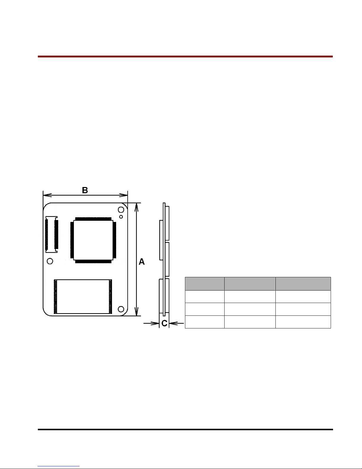
Dimensions
Side Millimeters Inches
A
40.00 ± 0.30 1.575 ± 0.012
B
30.00 ± 0.20 1.181 ± 0.008
C
5.00 ± 0.50 0.196 ± 0.020
Page 2
T
T
T
S
S
S
6
6
6
4
4
4
G
G
G
S
S
S
S
S
S
D
D
D
1
1
1
0
0
0
-
-
-
M
M
M
1.0” Solid State Disk
Transcend Information Inc.
V1.6
7
Specifications
* Note: Reference to the IEC 60068-2-1 and IEC 60068-2-56 Testing procedures; 48-hours chamber test on ASUS
M2N-MX, 1GB RAM, Windows® XP Version 2002 SP2.
Physical Specification
Form Factor
1-inch HDD
Storage Capacities
64 GB
Length
30.0 0 ± 0.20
Width
40.00 ± 0.30
Dimensions (mm)
Height
5.00 ± 0.50
Weight
8 g
Connector
0.3 mm pitch 35-Pin Zero Insertion Force (ZIF) connector (P-ATA)
Environmental Specifications
Operating Temperature
0 ℃ to 70 ℃
Storage Temperature
0 ℃ to 70 ℃
Humidity
Operating Humidity (Non condensation)
0% to 95%
Storage Humidity (Non condensation)
0% to 95%
Power Consumption
Input Voltage
DC 3.3V ± 5%
Mode Maximum (mA)
Write
143
Read
119
Power Consumption
(DC 3.3V @25℃)
Standby
3.8
Page 3
T
T
T
S
S
S
6
6
6
4
4
4
G
G
G
S
S
S
S
S
S
D
D
D
1
1
1
0
0
0
-
-
-
M
M
M
1.0” Solid State Disk
Transcend Information Inc.
V1.6
8
* Note : 25 ℃, test on ASUS M3N7B, 3GB RAM, IDE interface support UDMA5, Windows® XP SP3, benchmark utility
FDBENCH (version 1.02), copied file 100MB
Actual Capacity
Model P/N User LBA Cylinder Head Sector
TS64GSSD10-M 125,059,072 16383 15 63
* Note: FAT32 format
Reliability
Data Reliability
Random 8-bit BCH ECC in 512 bytes
Data Retention
10 years [7 years operating (block erase cycle < 4K cycle) + 3 years storage]
Connector Durability
10 times
MTBF
4,400,000 hours
Interface Specification
Drivers
No Device Driver Required
ATA-7 V3 Specification
PIO Mode 0 - 4
Multi-Word DMA Mode 0 -2
ATA Compatibility
UDMA Mode 0 - 5
Performance
Model P/N Capacity Read Write Random Read Random Write
PCMark05
HDD Score
TS64GSSD10-M 64GB 64851 39233 56952 11297 6358
Regulations
Compliance
CE, FCC and BSMI
Page 4
T
T
T
S
S
S
6
6
6
4
4
4
G
G
G
S
S
S
S
S
S
D
D
D
1
1
1
0
0
0
-
-
-
M
M
M
1.0” Solid State Disk
Transcend Information Inc.
V1.6
9
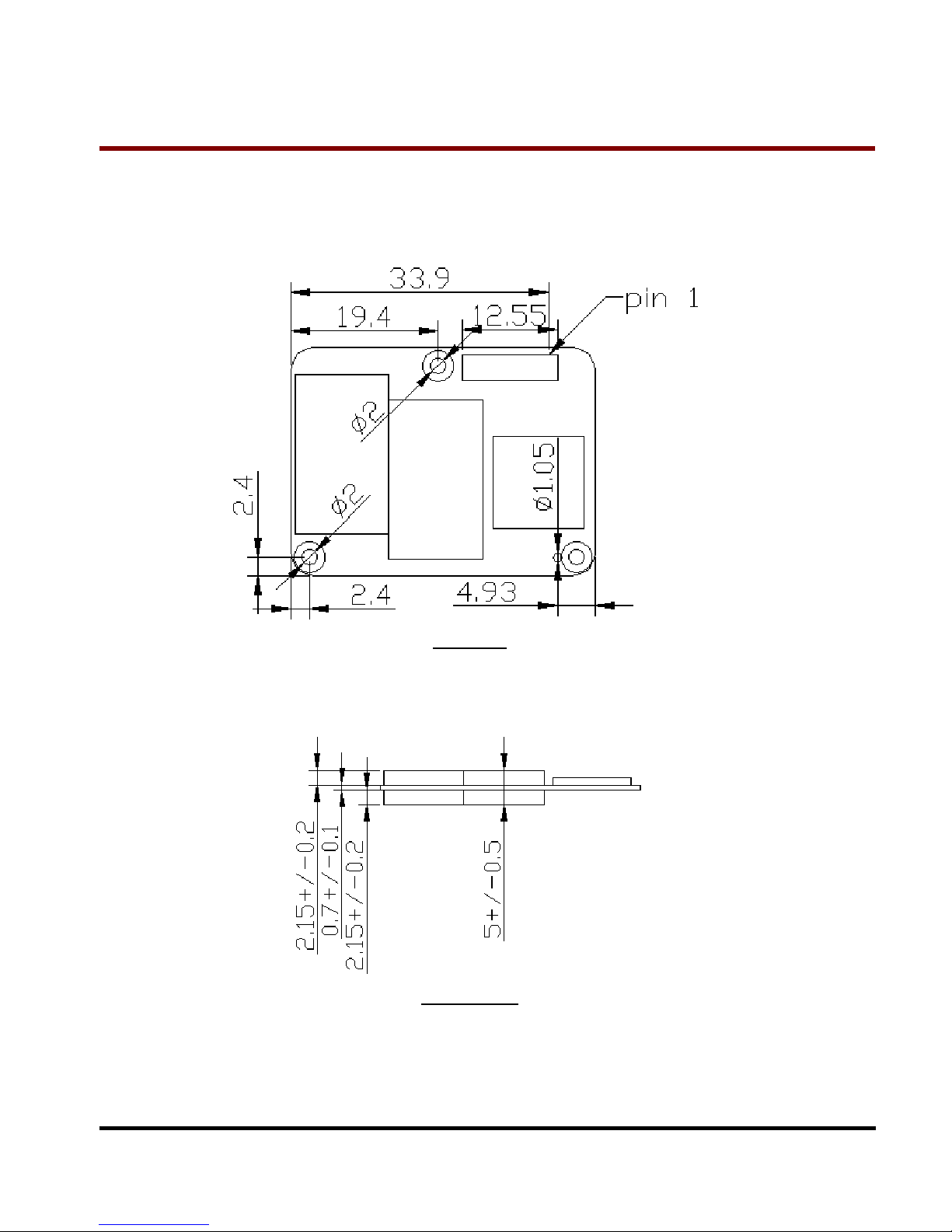
Mechanical Dimensions
Below figure illustrates the Transcend 1” Solid State Disk. All dimensions are in mm.
Top View
Lateral View
Page 5
T
T
T
S
S
S
6
6
6
4
4
4
G
G
G
S
S
S
S
S
S
D
D
D
1
1
1
0
0
0
-
-
-
M
M
M
1.0” Solid State Disk
Transcend Information Inc.
V1.6
10
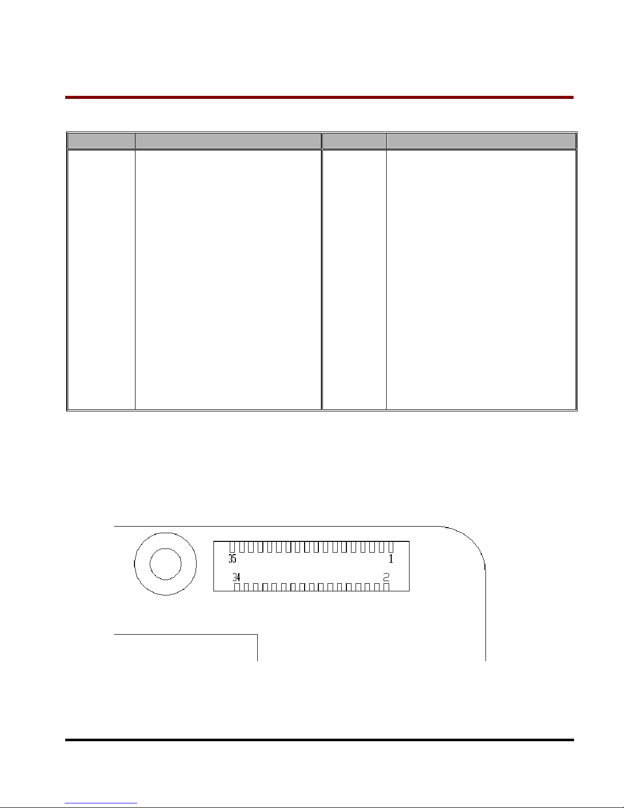
Pin Assignments
Pin No. Pin Name Pin No. Pin Name
01 GND 02 DD10
03 DD9 04 DD2
05 DD8 06 DD1
07 -PDIAG 08 DD0
09 -DASP 10 DA0
11 -DMACK 12 DA1
13 DMARQ 14 DA2
15 DSTROBE 16 -RESET
17 -CSEL 18 VCC
19 VCC 20 INTRQ
21 -HIOW 22 -HIOR
23 -CS1 24 -CS0
25 DD15 26 DD7
27 DD14 28 DD6
29 DD13 30 DD5
31 DD12 32 DD4
33 DD11 34 DD3
35 GND
Pin Layout
Page 6
T
T
T
S
S
S
6
6
6
4
4
4
G
G
G
S
S
S
S
S
S
D
D
D
1
1
1
0
0
0
-
-
-
M
M
M
1.0” Solid State Disk
Transcend Information Inc.
V1.6
11
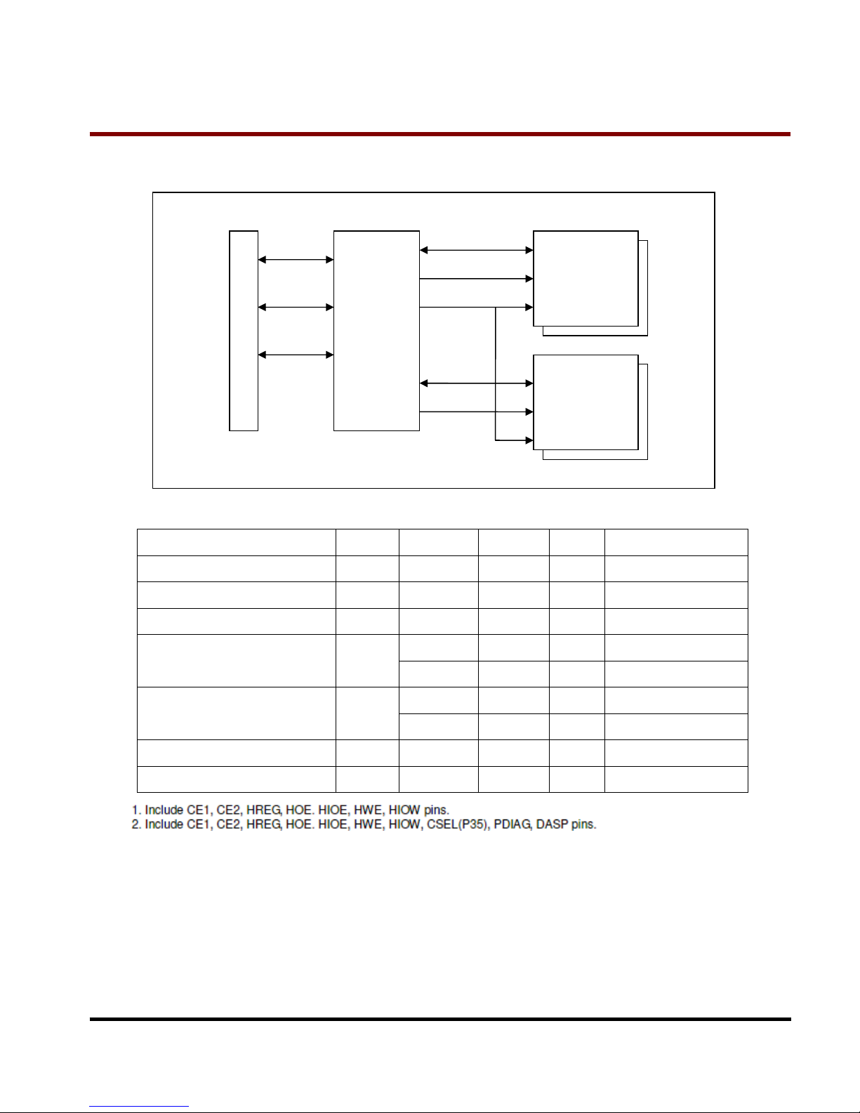
Block Diagram
DC Characteristics
Parameter Symbol
Min. Max. Unit Remark
Supply Voltage VCC 2.97 3.63 V
High level output voltage VOH V
CC
– 0.8 V
Low level output voltage VOL 0.8 V
2.4 V Non-schmitt trigger
High level input voltage
VIH
2.05 V Schmitt trigger1
0.6 V Non-schmitt trigger
Low level input voltage
VIL
1.25 V Schmitt trigger1
Pull up resistance2 RPU 52.7 141 KOhm
Pull down resistance RPD 47.5 172 kOhm
Solid
State Disk
Controller
Flash Memory
D0 – D7
-CE0
-CE1
-WE…-RE
35
PIN
FPC
Connector
Flash Memory
D0 – D7
-CE0
-CE1
-WE…-RE
D00 ~ D07
D10 ~ D17
-
CE0, -CE2…
-
CE1, -CE3…
Data bus
Control
Signal
Power
Others
Page 7
T
T
T
S
S
S
6
6
6
4
4
4
G
G
G
S
S
S
S
S
S
D
D
D
1
1
1
0
0
0
-
-
-
M
M
M
1.0” Solid State Disk
Transcend Information Inc.
V1.6
12
DC Characteristics
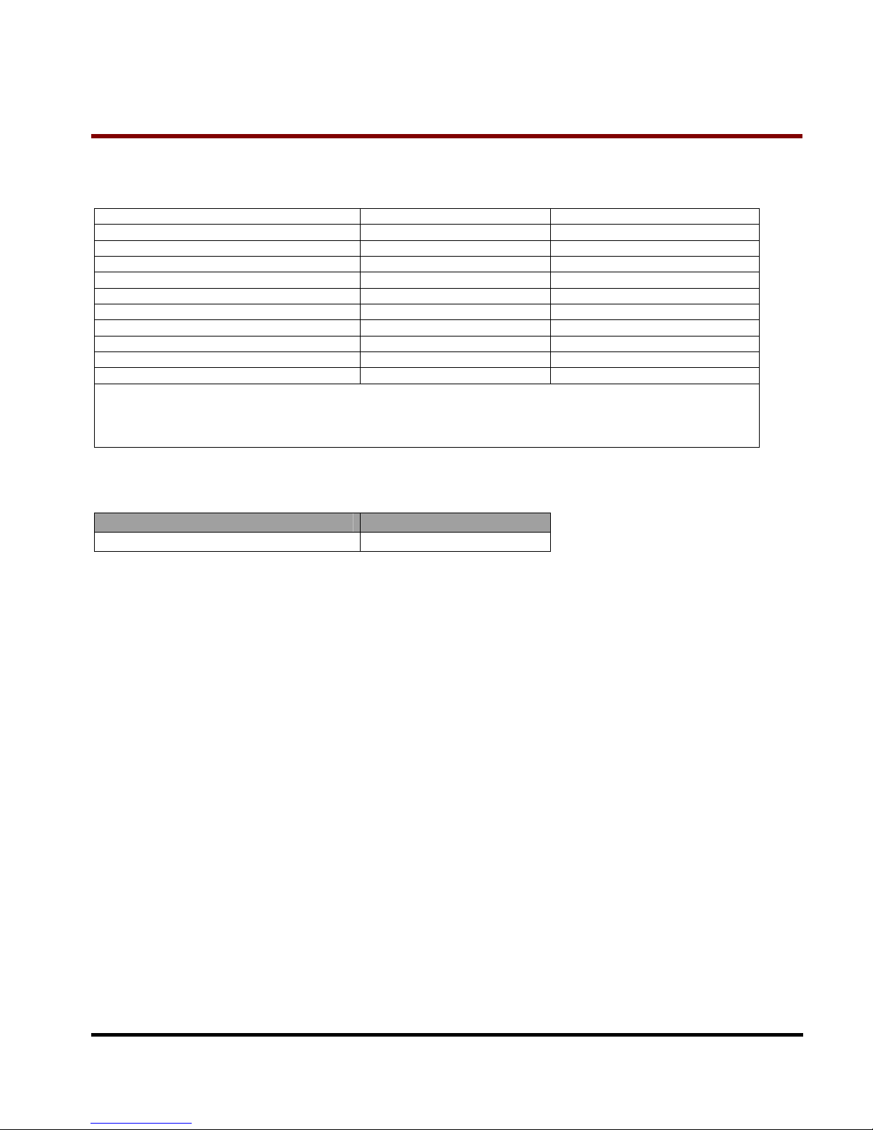
Table: Series Termination for Ultra DMA
Signal Host Termination Device Termination
-IORD (-HDMARDY,HSTROBE) 22 ohm 88 ohm
-IOWR (STOP) 22 ohm 88 ohm
-CS0, -CS1 33 ohm 88 ohm
A00, A01, A02 33 ohm 88 ohm
-DMACK 22 ohm 88 ohm
D15 through D00 33 ohm 33 ohm
DMARQ 82 ohm 22 ohm
INTRQ 82 ohm 22 ohm
DSTROBE (-DDMARDY, DSTROBE) 82 ohm 22 ohm
-RESET 33 ohm 88 ohm
NOTE − Only those signals requiring termination are listed in this table. If a signal is not listed, series
termination is not required for operation in an Ultra DMA mode. Shows signals also requiring a pull-up or
pull-down resistor at the host. The actual termination values should be selected to compensate for transceiver
and trace impedance to match the characteristic cable impedance.
Electrical Characteristics
Parameter Value
Frequency Stability 30-80MHz
Page 8
T
T
T
S
S
S
6
6
6
4
4
4
G
G
G
S
S
S
S
S
S
D
D
D
1
1
1
0
0
0
-
-
-
M
M
M
1.0” Solid State Disk
Transcend Information Inc.
V1.6
13
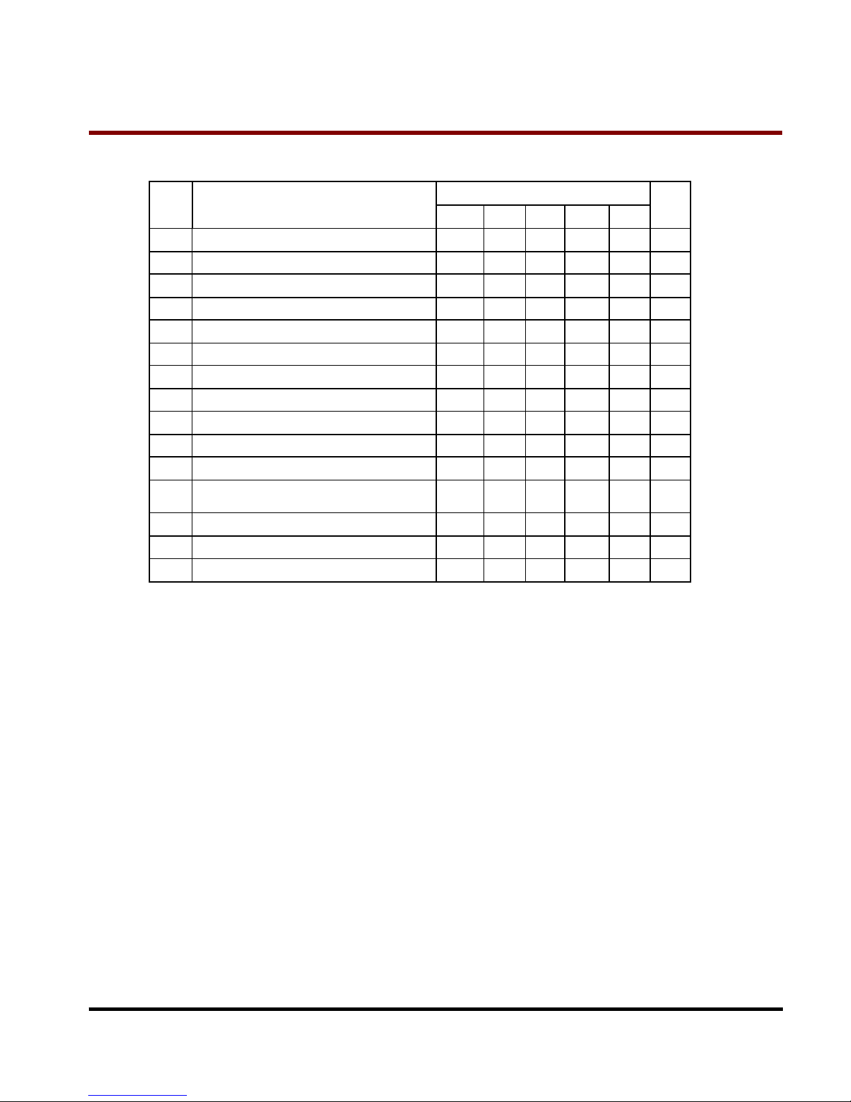
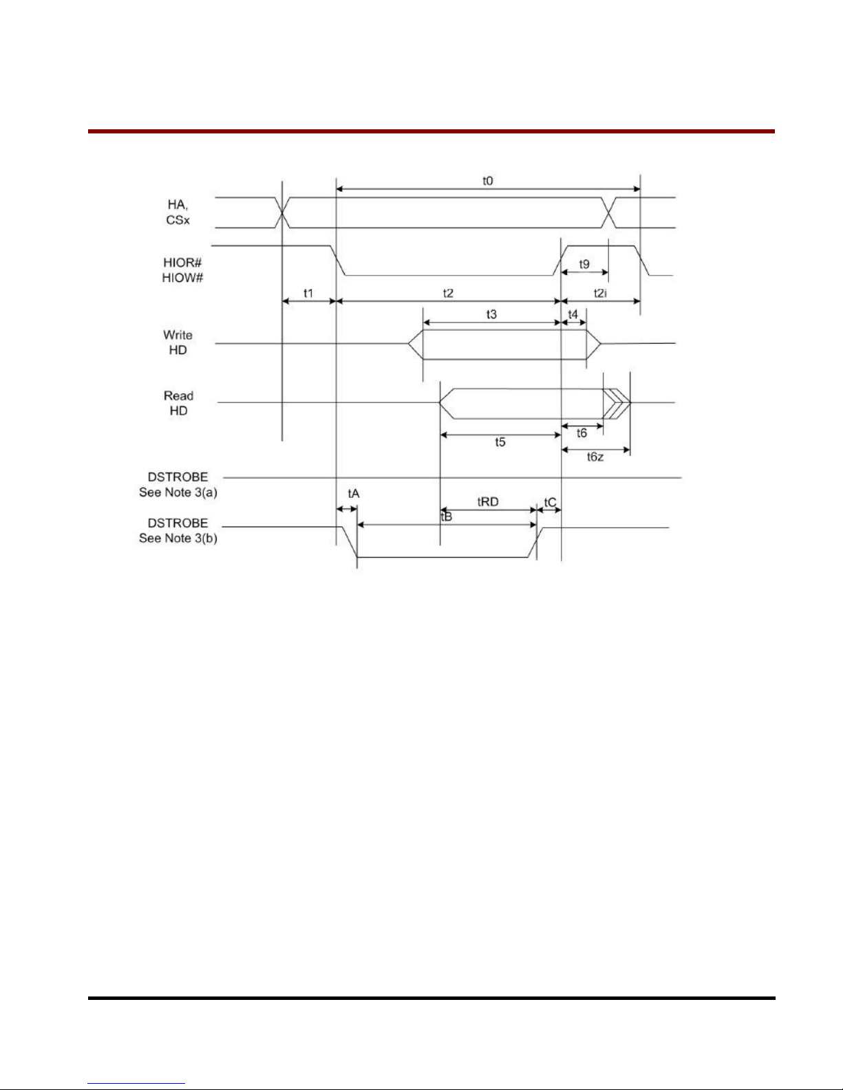
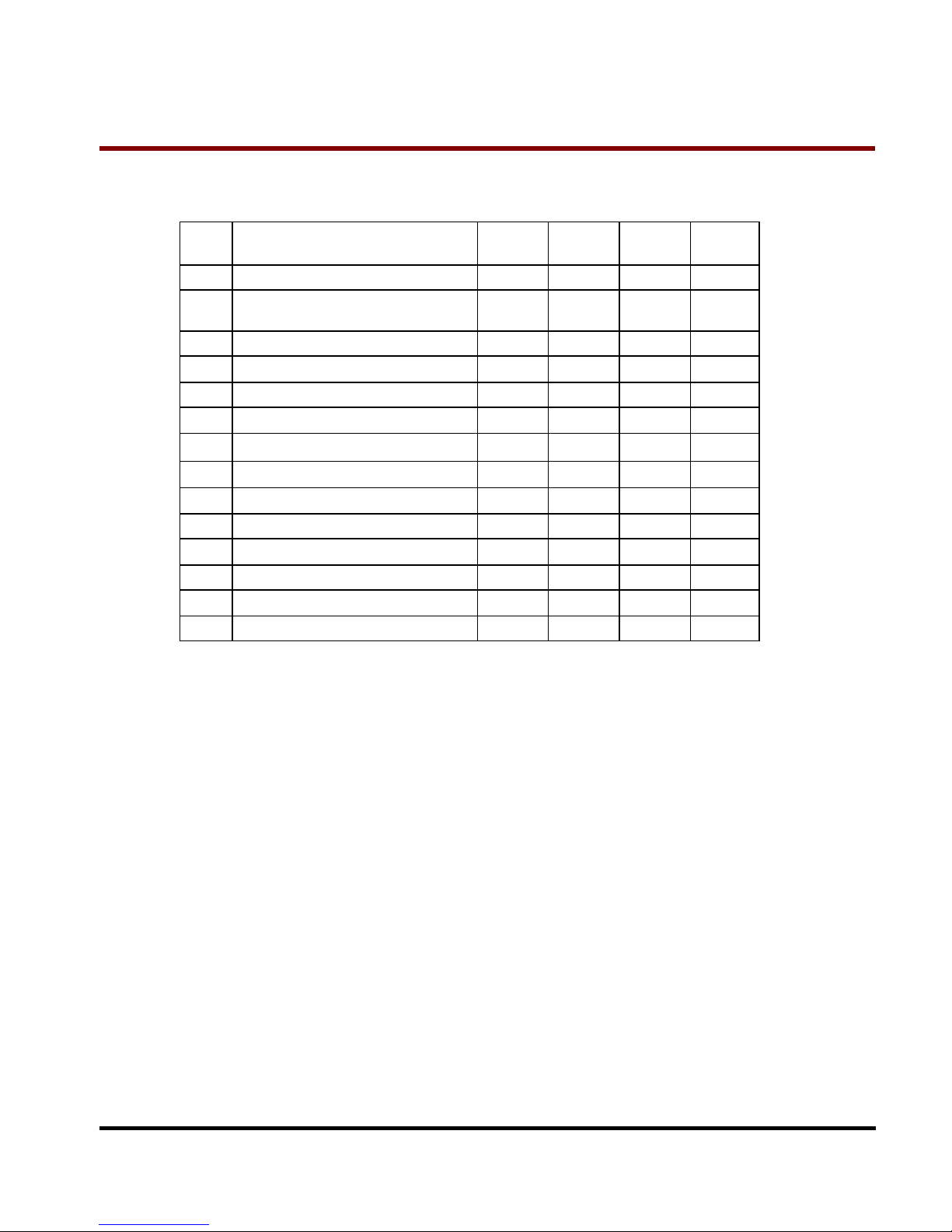
True IDE PIO Mode Read/Write Timing Specification
Mode
Item
0 1 2 3 4
Note
t0 Cycle time (min) 600 383 240 180 120 1
t1 Address Valid to -HIOR/-HIOW setup (min) 70 50 30 30 25
t2 -HIOR/-HIOW (min) 165 125 100 80 70 1
t2 -HIOR/-HIOW (min) Register (8 bit) 290 290 290 80 70 1
t2i -HIOR/-HIOW recovery time (min) - - - 70 25 1
t3 -HIOW data setup (min) 60 45 30 30 20
t4 -HIOW data hold (min) 30 20 15 10 10
t5 -HIOR data setup (min) 50 35 20 20 20
t6 -HIOR data hold (min) 5 5 5 5 5
t6Z -HIOR data tristate (max) 30 30 30 30 30 2
t9 -HIOR/-HIOW to address valid hold 20 15 10 10 10
tRD
Read Data Valid to DSTROBE active (min),
if DSTROBE initially low after tA
0 0 0 0 0
tA DSTROBE Setup time 35 35 35 35 35 3
tB DSTROBE Pulse Width (max) 1250 1250
1250
1250 1250
tC DSTROBE assertion to release (max) 5 5 5 5 5
Notes: All timings are in nanoseconds. All time intervals are recorded in nanoseconds. Although minimum time from DSTROBE high
to HIOR# high is 0 nsec, the minimum HIOR# width is still met.
1) Where t0 denotes the minimum total cycle time, t2 represents the minimum command active time, and t2i is the minimum
command recovery time or command inactive time. Actual cycle time equals the sum of the actual command active time and
the actual command inactive time. The three timing requirements of t0, t2, and t2i are met. The minimum total cycle time
requirement is greater than the sum of t2 and t2i, implying that a host implementation can extend either or both t2 or t2i to
ensure that t0 is equal to or greater than the value reported in the device’s identify device data. A PATA implementation
supports any legal host implementation.
2) This parameter specifies the time from the negation edge of HIOR# to the time that the PATA (tri-state) no longer drives the
data bus.
3) The delay from the activation of HIOR# or HIOW# activation until the state of DSTROBE is first sampled. If DSTROBE is
inactive, the host waits until DSTROBE is active before the PIO cycle is completed. When the PATA is not driving DSTROBE,
which is negated at the tA after HIOR# or HIOW# activation, then t5 is met and tRD is not applicable. When the PATA is
driving DSTROBE, which is negated at the time tA after HIOR# or HIOW#, then tRD is met and t5 is not applicable.
4) DSTROBE is not supported in this mode.
Page 9
T
T
T
S
S
S
6
6
6
4
4
4
G
G
G
S
S
S
S
S
S
D
D
D
1
1
1
0
0
0
-
-
-
M
M
M
1.0” Solid State Disk
Transcend Information Inc.
V1.6
14
NOTES:
1 Device address comprises CS1#, CS0#, and HA [2:0].
2 Data comprises HD [15:] (16-bit) or HD [7:0] (8 bit).
3 The negation of DSTROBE by the device is used to lengthen the PIO cycle. Whether the cycle is to be extended is
determined by the host after tA from the assertion of HIOR# or HIOW#. The assertion and negation of DSTROBE is
described in the following three cases:
(a) The device never negates DSTROBE: No wait is generated.
(b) Device drives DSTROBE low before tA: a wait is generated. The cycle is completed after DSTROBE is reasserted.
For cycles in which a wait is generated and HIOR# is asserted, the device places read data on D15-D00 for t
RD
before DSTROBE is asserted.
Page 10
T
T
T
S
S
S
6
6
6
4
4
4
G
G
G
S
S
S
S
S
S
D
D
D
1
1
1
0
0
0
-
-
-
M
M
M
1.0” Solid State Disk
Transcend Information Inc.
V1.6
15
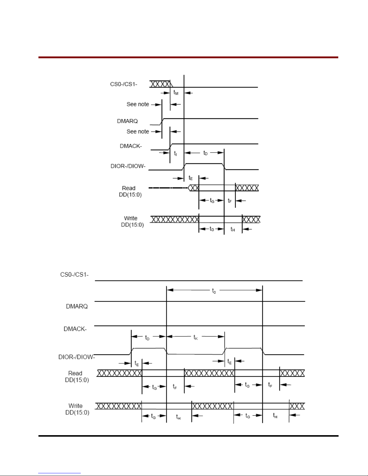
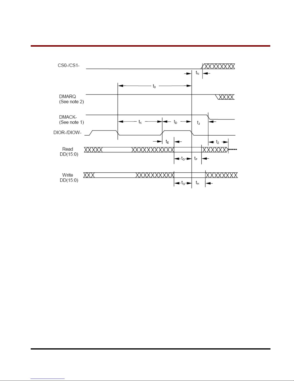
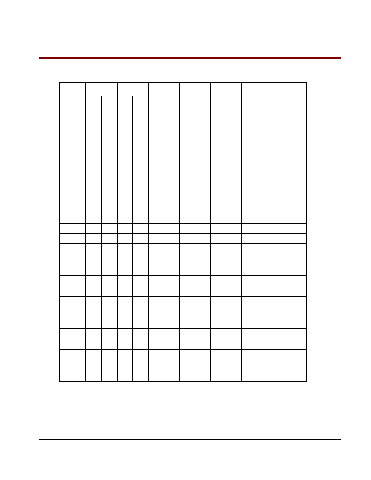
True IDE Multiword DMA Mode Read/Write Timing Specification
Item
Mode 0
(ns)
Mode 1
(ns)
Mode 2
(ns)
Note
t
O
Cycle time (min) 480 150 120 1
t
D
HIOR# / HIOW# asserted width (min) 215 80 70 1
t
E
HIOR# data access (max) 150 60 50
t
F
HIOR# data hold (min) 5 5 5
t
G
HIOR#/HIOW# data setup (min) 100 30 20
t
H
HIOW# data hold (min) 20 15 10
t
I
DMACK# to HIOR#/HIOW# setup (min)
0 0 0
t
J
HIOR# / HIOW# to DMACK# hold (min)
20 5 5
t
KR
HIOR# negated width (min) 50 50 25 1
t
KW
HIOW# negated width (min) 215 50 25 1
t
LR
HIOR# to DMARQ delay (max) 120 40 35
t
LW
HIOW# to DMARQ delay (max) 40 40 35
t
M
CSx valid to HIOR# / HIOW# 50 30 25
t
N
CSx hold 15 10 10
Page 11
T
T
T
S
S
S
6
6
6
4
4
4
G
G
G
S
S
S
S
S
S
D
D
D
1
1
1
0
0
0
-
-
-
M
M
M
1.0” Solid State Disk
Transcend Information Inc.
V1.6
16
Initiating a Multiword DMA data burst
NOTE-The host shall not assert DMACK- or negate both CS0 and CS1 until the assertion of DMARQ is detected. The
maximum time from the assertion of DMARQ to the assertion of DMACK- or the negation of both CS0 and CS1 is not
defined.
Sustaining a Multiword DMA data burst
Page 12
T
T
T
S
S
S
6
6
6
4
4
4
G
G
G
S
S
S
S
S
S
D
D
D
1
1
1
0
0
0
-
-
-
M
M
M
1.0” Solid State Disk
Transcend Information Inc.
V1.6
17
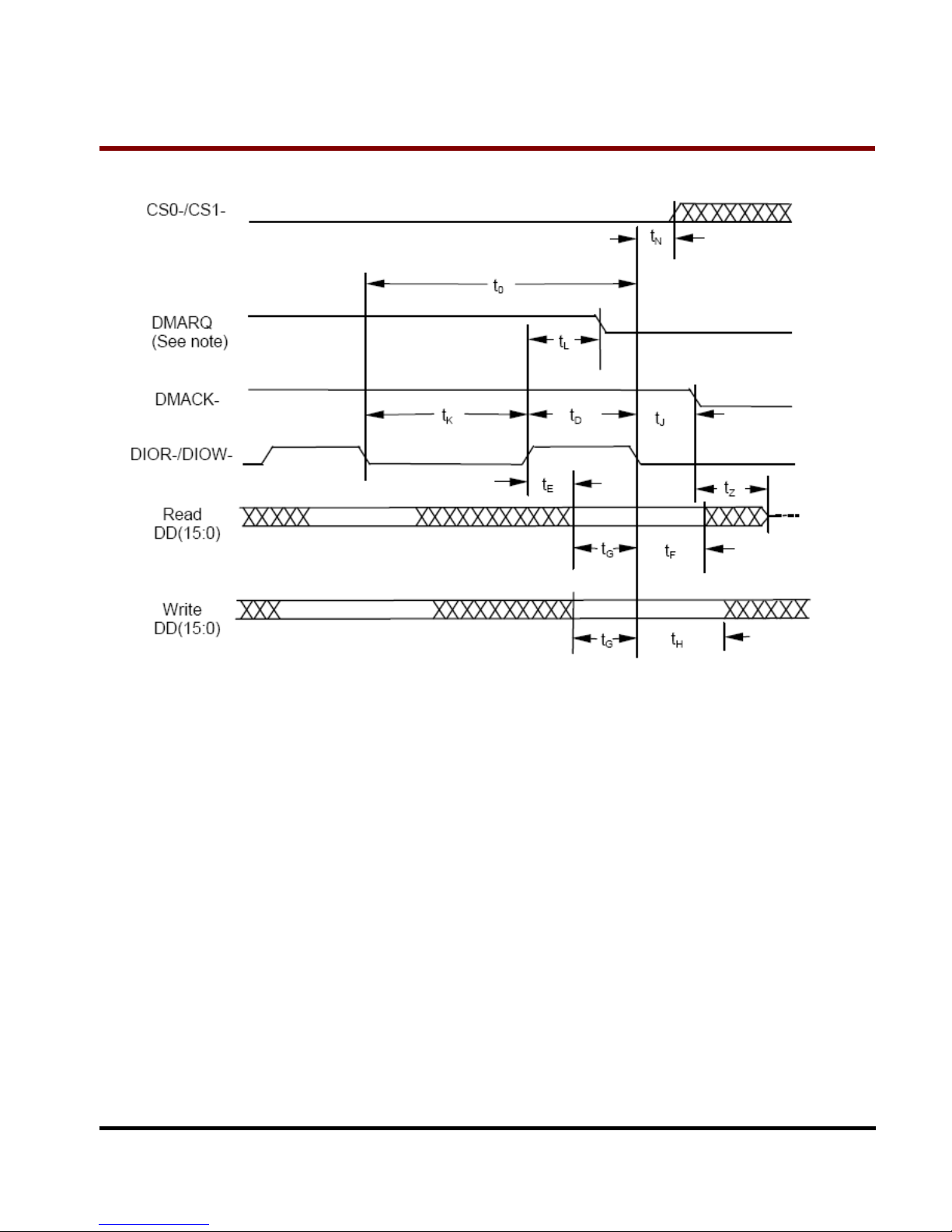
Device terminating a Multiword DMA data burst
NOTE:
To terminate the data burst, the Device shall negate DMARQ within the tL of the assertion of the current
HIOR- or HIOW- pulse. The last data word for the burst shall then be transferred by the negation of the
current HIOR- or HIOW- pulse. If all data for the command has not been transferred, the device shall
reassert DMARQ again at any later time to resume the DMA operation as shown in figure True IDE PIO
Mode Read/Write Timing.
Page 13
T
T
T
S
S
S
6
6
6
4
4
4
G
G
G
S
S
S
S
S
S
D
D
D
1
1
1
0
0
0
-
-
-
M
M
M
1.0” Solid State Disk
Transcend Information Inc.
V1.6
18
Host terminating a Multiword DMA data burst
NOTE:
1.To terminate the transmission of a data burst, the host shall negate DMACK- within tJ after a HIOR or
HIOW- pulse. No further HIOR- or HIOW- pulses shall be asserted for this burst.
2. If the device is able to continue the transfer of data, the device may leave DMARQ asserted and wait for
the host to reassert DMACK- or may negate DMARQ at any time after detecting that DMACK has been
negated.
Page 14
T
T
T
S
S
S
6
6
6
4
4
4
G
G
G
S
S
S
S
S
S
D
D
D
1
1
1
0
0
0
-
-
-
M
M
M
1.0” Solid State Disk
Transcend Information Inc.
V1.6
19
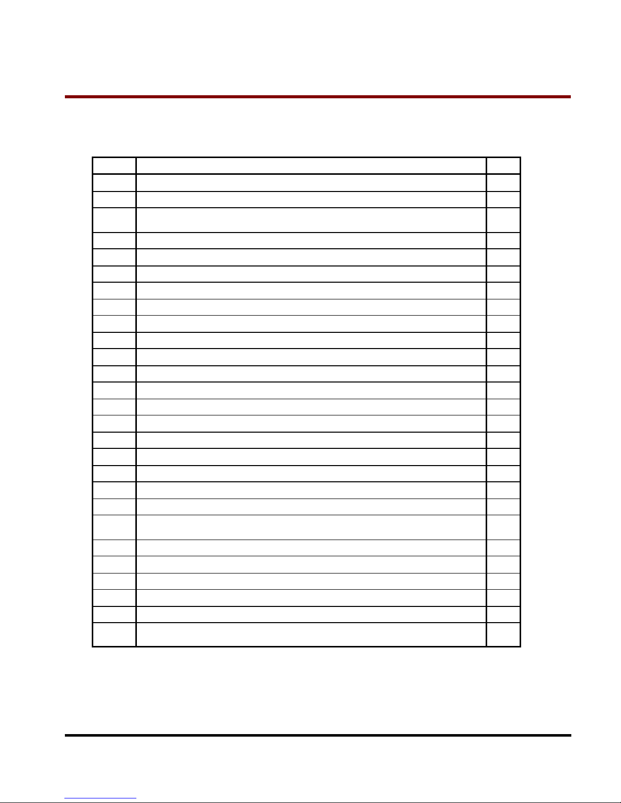
True IDE Ultra DMA Mode Read/Write Timing Specification
Notes:
1) All timing measurement switching points (low to high and high to low) shall be taken at 1.5 V.
2) All signal transitions for a timing parameter shall be measured at the connector specified in the measurement
location column. For example, in the case of tRFS, both STROBE and –DMARDY transitions are measured at the
sender connector.
3) The parameter tCYC shall be measured at the recipient’s connector farthest from the sender.
4) The parameter tLI shall be measured at the connector of the sender or recipient that is responding to an
incoming transition from the recipient or sender respectively. Both the incoming signal and the outgoing
Name
UDMA
Mode 0
UDMA
Mode 1
UDMA
Mode 2
UDMA
Mode 3
UDMA
Mode 4
UDMA
Mode 5
Min Max Min Max Min Max Min Max Min Max Min Max
Measure
location (see
Note 2)
t
2CYCTYP
240 160 120 90
60
40 Sender
t
CYC
112 73
54
39
25
16.8 Note 3
t
2CYC
230 153 115 86
57
38 Sender
t
DS
15.0 10.0 7.0
7.0
5.0
4.0
Recipient
t
DH
5.0
5.0
5.0
5.0
5.0
4.6
Recipient
t
DVS
70.0 48.0 31.0 20.0 6.7
4.8
Sender
t
DVH
6.2
6.2
6.2
6.2
6.2
4.8
Sender
t
CS
15.0 10.0 7.0
7.0
5.0
5.0
Device
t
CH
5.0
5.0
5.0
5.0
5.0
5.0
Device
t
CVS
70.0 48.0 31.0 20.0 6.7
10.0 Host
t
CVH
6.2
6.2
6.2
6.2
6.2
10.0 Host
t
ZFS
0 0 0 0 0 35 Device
t
DZFS
70.0 48.0 31.0 20.0 6.7
25 Sender
t
FS
230
200 170 130 120 90 Device
t
LI
0 150 0 150 0 150 0 100 0 100 0 75 Note 4
t
MLI
20
20
20
20
20
20 Host
t
UI
0 0 0 0 0 0 Host
t
AZ
10
10
10
10
10 10 Note 5
t
ZAH
20
20
20
20
20
20 Host
t
ZAD
0 0 0 0 0 0 Device
t
ENV
20 70 20 70 20 70 20 55 20 55 20 50 Host
t
RFS
75
70
60
60
60 50 Sender
t
RP
160 125 100 100 100 85 Recipient
t
DSTROBEZ
20
20
20
20
20 20 Device
t
ZDSTROBE
0 0 0 0 0 0 Device
t
ACK
20
20
20
20
20
20 Host
t
SS
50
50
50
50
50
50 Sender
Page 15
T
T
T
S
S
S
6
6
6
4
4
4
G
G
G
S
S
S
S
S
S
D
D
D
1
1
1
0
0
0
-
-
-
M
M
M
1.0” Solid State Disk
Transcend Information Inc.
V1.6
20
response shall be measured at the same connector.
5) The parameter tAZ shall be measured at the connector of the sender or recipient that is driving the bus but must
release the bus to allow for a bus turnaround.
Name Comment Notes
t
2CYCTYP
Typical sustained average two cycle time
t
CYC
Cycle time allowing for asymmetry and clock variations (from STROBE edge to STROBE edge)
t
2CYC
Two cycle time allowing for clock variations (from rising edge to next rising edge or from falling edge to
next falling edge of STROBE)
t
DS
Data setup time at recipient (from data valid until STROBE edge) 2, 5
t
DH
Data hold time at recipient (from STROBE edge until data may become invalid) 2, 5
t
DVS
Data valid setup time at sender (from data valid until STROBE edge) 3
t
DVH
Data valid hold time at sender (from STROBE edge until data may become invalid) 3
t
CS
CRC word setup time at device 2
t
CH
CRC word hold time device 2
t
CVS
CRC word valid setup time at host (from CRC valid until -DMACK negation) 3
t
CVH
CRC word valid hold time at sender (from -DMACK negation until CRC may become invalid) 3
t
ZFS
Time from STROBE output released-to-driving until the first transition of critical timing.
t
DZFS
Time from data output released-to-driving until the first transition of critical timing.
t
FS
First STROBE time (for device to first negate DSTROBE from STOP during a data in burst)
t
LI
Limited interlock time 1
t
MLI
Interlock time with minimum 1
t
UI
Unlimited interlock time 1
t
AZ
Maximum time allowed for output drivers to release (from asserted or negated)
t
ZAH
Minimum delay time required for output
t
ZAD
drivers to assert or negate (from released)
t
ENV
Envelope time (from -DMACK to STOP and -HDMARDY during data in burst initiation and from
DMACK to STOP during data out burst initiation)
t
RFS
Ready-to-final-STROBE time (no STROBE edges shall be sent this long after negation of -DMARDY)
t
RP
Ready-to-pause time (that recipient shall wait to pause after negating -DMARDY)
t
DSTROBEZ
Maximum time before releasing DSTROBE 6
t
ZDSTROBE
Minimum time before driving DSTROBE 4, 6
t
ACK
Setup and hold times for -DMACK (before assertion or negation)
t
SS
Time from STROBE edge to negation of DMARQ or assertion of STOP (when sender terminates a
burst)
Page 16
T
T
T
S
S
S
6
6
6
4
4
4
G
G
G
S
S
S
S
S
S
D
D
D
1
1
1
0
0
0
-
-
-
M
M
M
1.0” Solid State Disk
Transcend Information Inc.
V1.6
21
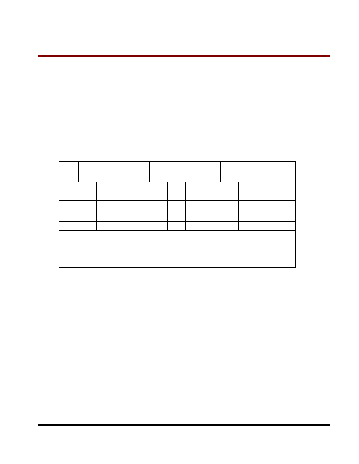
Notes: 1) The parameters tUI, tMLI : (Ultra DMA Data-In Burst Device Termination Timing and Ultra DMA Data-In
Burst Host Termination Timing), and tLI indicate sender-to-recipient or recipient-to-sender interlocks, i.e., one agent
(either sender or recipient) is waiting for the other agent to respond with a signal before proceeding. tUI is an
unlimited interlock that has no maximum time value. tMLI is a limited time-out that has a defined minimum. tLI is a
limited time-out that has a defined maximum.
2) 80-conductor cabling shall be required in order to meet setup (tDS, tCS) and hold (tDH, tCH) times
in modes greater than 2.
3) Timing for tDVS, tDVH, tCVS and tCVH shall be met for lumped capacitive loads of 15 and 40 pF at
the connector where the Data and STROBE signals have the same capacitive load value. Due to
reflections on the cable, these timing measurements are not valid in a normally functioning system.
4) For all modes the parameter tZDSTROBE may be greater than tENV due to the fact that the host
has a pull-up on DSTROBE- giving it a known state when released.
5) The parameters tDS, and tDH for mode 5 are defined for a recipient at the end of the cable only in a
configuration with a single device located at the end of the cable. This could result in the minimum
values for tDS and tDH for mode 5 at the middle connector being 3.0 and 3.9 ns respectively.
Name
UDMA
Mode 0 (ns)
UDMA
Mode 1 (ns)
UDMA
Mode 2 (ns)
UDMA
Mode 3 (ns)
UDMA
Mode 4 (ns)
UDMA
Mode 5 (ns)
Min Max Min Max Min Max Min Max Min Max Min Max
t
DSIC
14.7
9.7
6.8
6.8
4.8
2.3
t
DHIC
4.8
4.8
4.8
4.8
4.8
2.8
t
DVSIC
72.9
50.9
33.9
22.6
9.5
6.0
t
DVHIC
9.0
9.0
9.0
9.0
9.0
6.0
t
DSIC
Recipient IC data setup time (from data valid until STROBE edge) (see note 2)
t
DHIC
Recipient IC data hold time (from STROBE edge until data may become invalid) (see note 2)
t
DVSIC
Sender IC data valid setup time (from data valid until STROBE edge) (see note 3)
t
DVHIC
Sender IC data valid hold time (from STROBE edge until data may become invalid) (see note 3)
Notes: 1) All timing measurement switching points (low to high and high to low) shall be taken at 1.5 V.
2) The correct data value shall be captured by the recipient given input data with a slew rate of 0.4 V/ns
rising and falling and the input STROBE with a slew rate of 0.4 V/ns rising and falling at tDSIC and
tDHIC timing (as measured through 1.5 V).
3) The parameters tDVSIC and tDVHIC shall be met for lumped capacitive loads of 15 and 40 pF at the
IC where all signals have the same capacitive load value. Noise that may couple onto the output
signals from external sources has not been included in these values.
Page 17
T
T
T
S
S
S
6
6
6
4
4
4
G
G
G
S
S
S
S
S
S
D
D
D
1
1
1
0
0
0
-
-
-
M
M
M
1.0” Solid State Disk
Transcend Information Inc.
V1.6
22
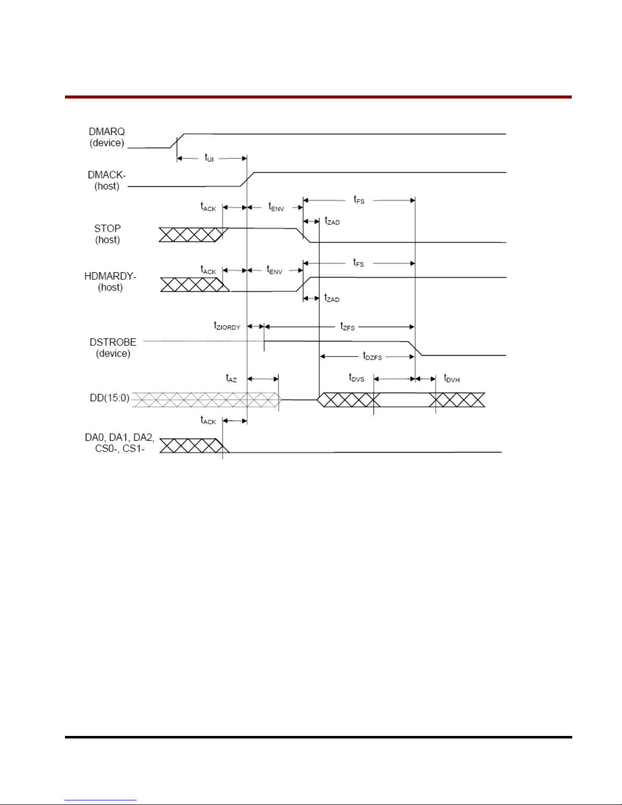
Initiating an Ultra DMA data-in burst
Note:
The definitions for the HIOW-:STOP, HIOR-:HDMARDY-:HSTROBE, and DSTROBE:DDMARDY-:DSTROBE
signal lines are not in effect until DMARQ and DMACK are asserted.
Page 18
T
T
T
S
S
S
6
6
6
4
4
4
G
G
G
S
S
S
S
S
S
D
D
D
1
1
1
0
0
0
-
-
-
M
M
M
1.0” Solid State Disk
Transcend Information Inc.
V1.6
23
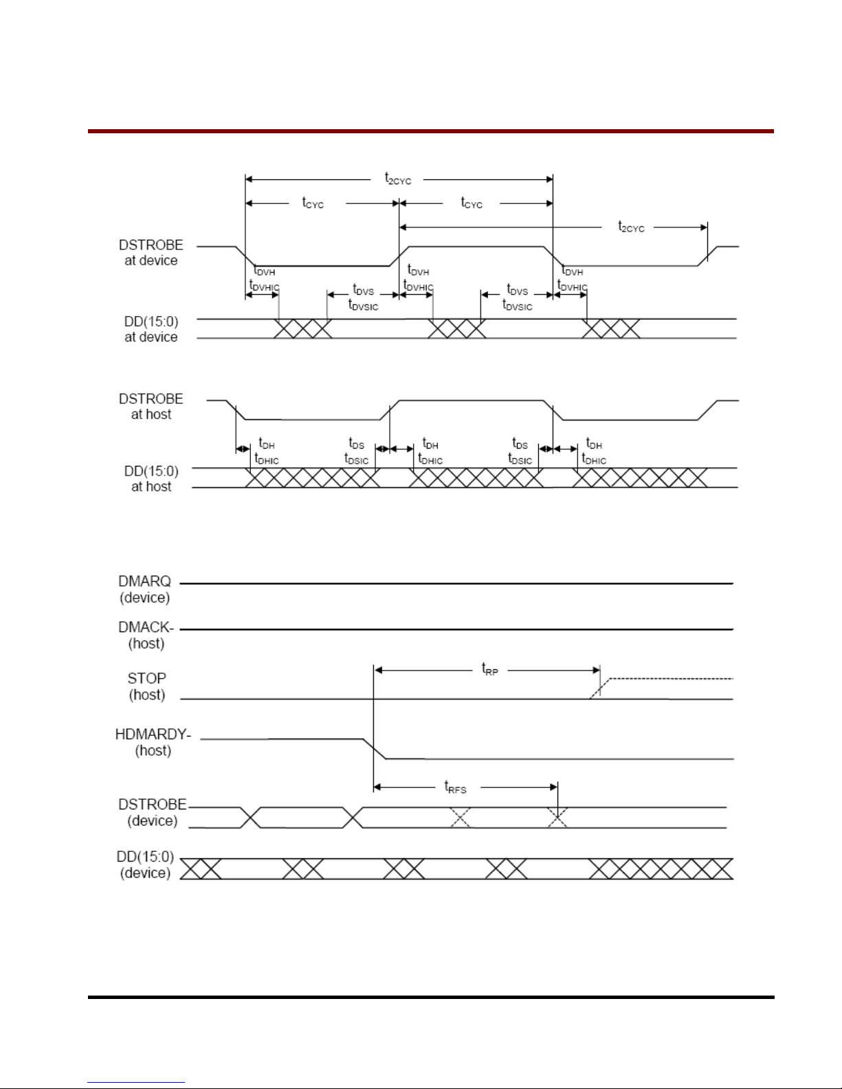
Sustained Ultra DMA data-in burst
Note:
The definitions for the HIOW-:STOP, HIOR-:HDMARDY-:HSTROBE and DSTROBE:DDMARDY-:DSTROBE
signal lines are not in effect until DMARQ and DMACK are asserted.
Host pausing an Ultra DMA data-in burst
Note:
1.The host may assert STOP to request termination of the Ultra DMA burst no sooner than t
RP
after
HDMARDY- is negated.
2.After negating HDMARDY-, the host may receive zero, one, two, or three more data words from the device.
Page 19
T
T
T
S
S
S
6
6
6
4
4
4
G
G
G
S
S
S
S
S
S
D
D
D
1
1
1
0
0
0
-
-
-
M
M
M
1.0” Solid State Disk
Transcend Information Inc.
V1.6
24
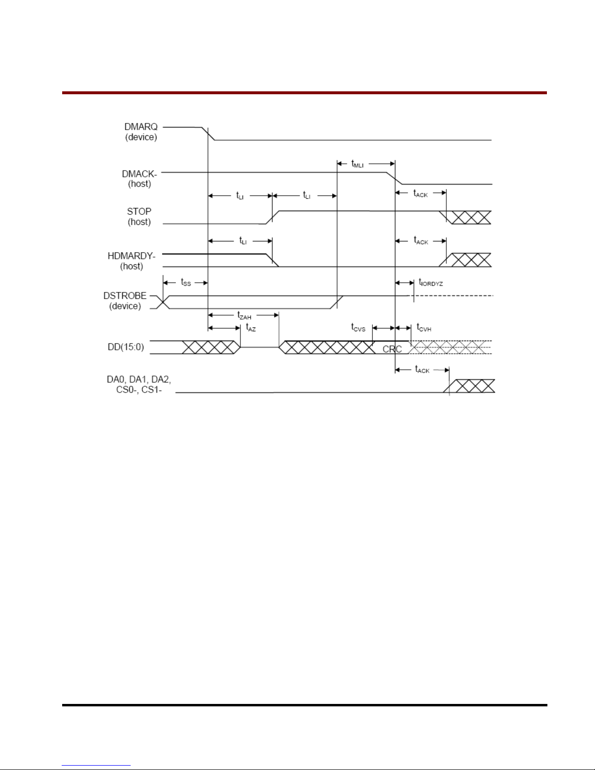
Device terminating an Ultra DMA data-in burst
Note:
The definitions for the STOP, HDMARDY, and DSTROBE signal lines are no longer in effect after DMARQ and
DMACK are negated.
Page 20
T
T
T
S
S
S
6
6
6
4
4
4
G
G
G
S
S
S
S
S
S
D
D
D
1
1
1
0
0
0
-
-
-
M
M
M
1.0” Solid State Disk
Transcend Information Inc.
V1.6
25
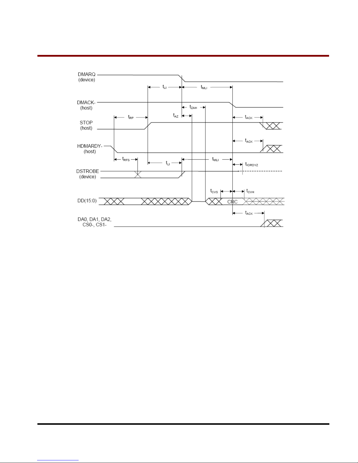
Host terminating an Ultra DMA data-in burst
Note:
The definitions for the STOP, HDMARDY, and DSTROBE signal lines are no longer in effect after DMARQ and
DMACK are negated.
Page 21
T
T
T
S
S
S
6
6
6
4
4
4
G
G
G
S
S
S
S
S
S
D
D
D
1
1
1
0
0
0
-
-
-
M
M
M
1.0” Solid State Disk
Transcend Information Inc.
V1.6
26
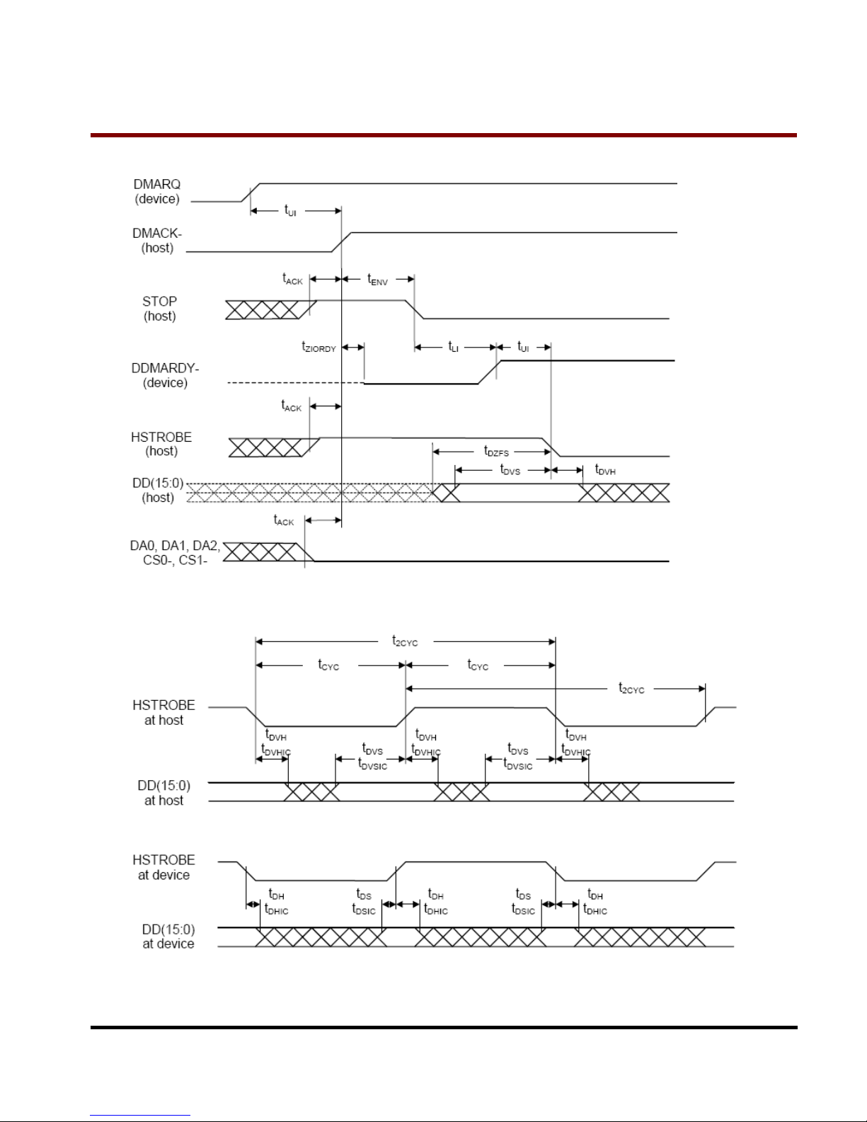
Initiating an Ultra DMA data-out burst
Note: The definitions for the STOP, DDMARDY, and HSTROBE signal lines are not in effect until DMARQ and
DMACK are asserted.
Sustained Ultra DMA data-out burst
Note: DD(15:0) and HSTROBE signals are shown at both the device and the host to emphasize that cable settling time
as well as cable propagation delay shall not allow the data signals to be considered stable at the device until some time
after they are driven by the host.
Page 22
T
T
T
S
S
S
6
6
6
4
4
4
G
G
G
S
S
S
S
S
S
D
D
D
1
1
1
0
0
0
-
-
-
M
M
M
1.0” Solid State Disk
Transcend Information Inc.
V1.6
27
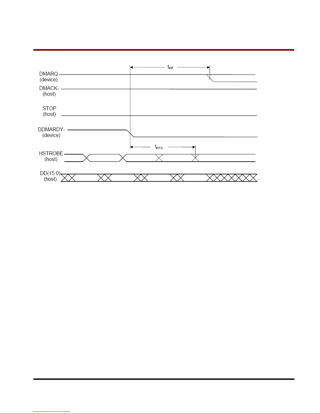
Device pausing an Ultra DMA data-out burst
Note:
1.The device may negate DMARQ to request termination of the Ultra DMA burst no sooner than t
RP
after
DDMARDY- is negated.
2 After negating DDMARDY-, the device may receive zero, one, two, or three more data words from the host.
Page 23
T
T
T
S
S
S
6
6
6
4
4
4
G
G
G
S
S
S
S
S
S
D
D
D
1
1
1
0
0
0
-
-
-
M
M
M
1.0” Solid State Disk
Transcend Information Inc.
V1.6
28
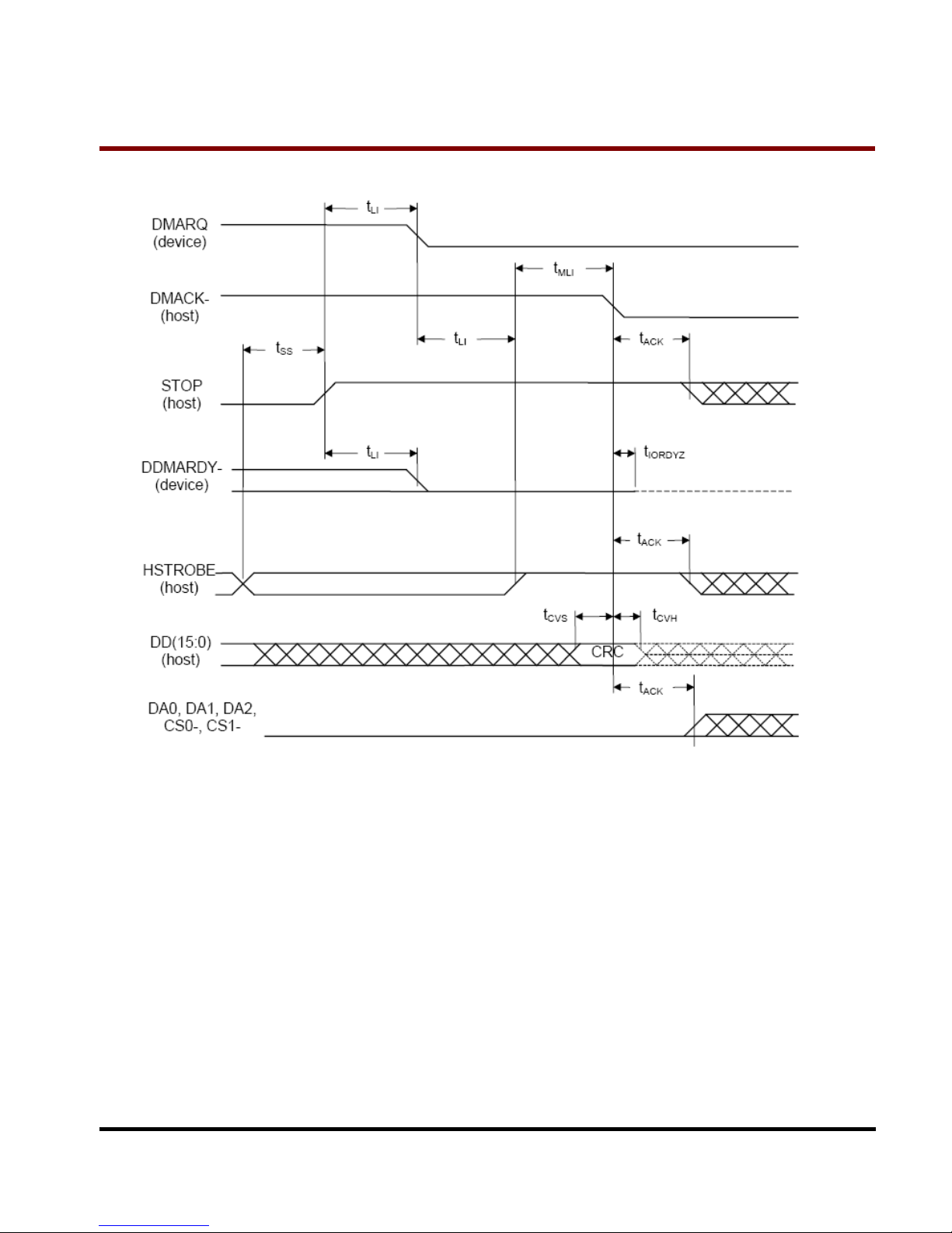
Host terminating an Ultra DMA data-out burst
Note:
The definitions for the STOP, DDMARDY, and HSTROBE signal lines are no longer in effect after DMARQ and
DMACK are negated.
Page 24
T
T
T
S
S
S
6
6
6
4
4
4
G
G
G
S
S
S
S
S
S
D
D
D
1
1
1
0
0
0
-
-
-
M
M
M
1.0” Solid State Disk
Transcend Information Inc.
V1.6
29
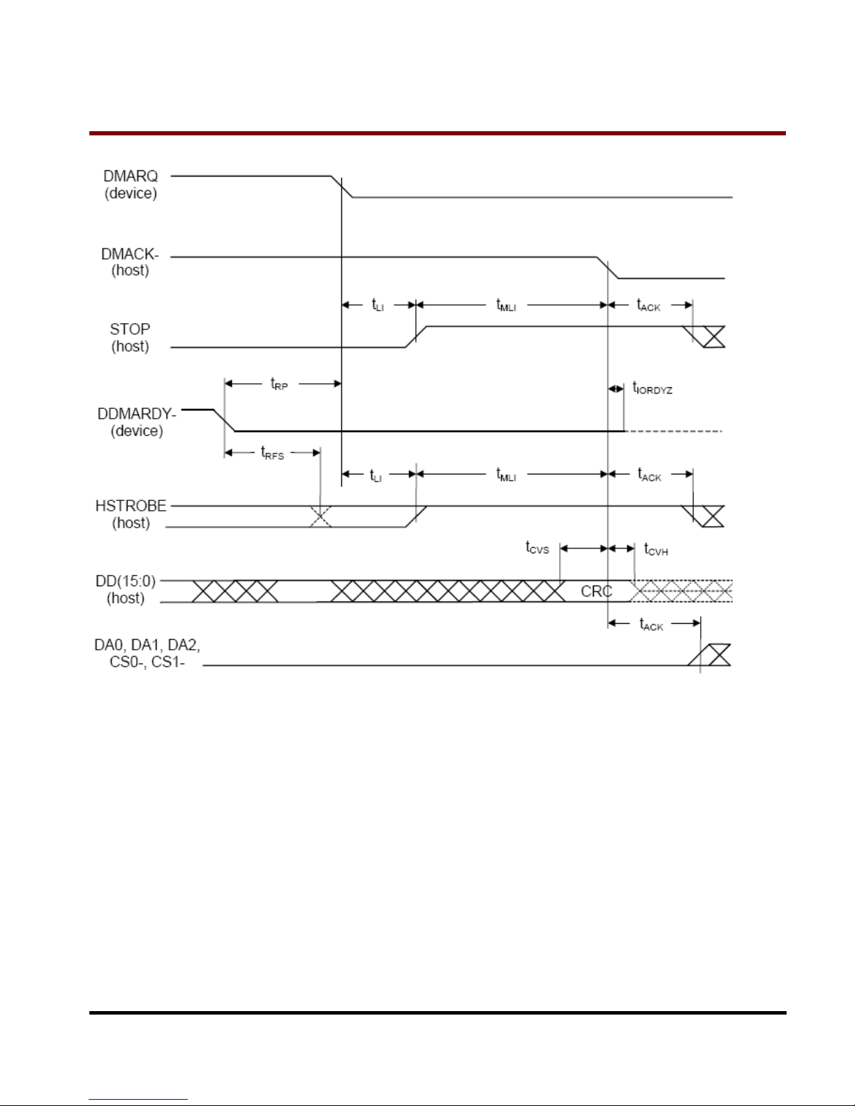
Device terminating an Ultra DMA data-out burst
Note:
The definitions for the STOP, DDMARDY, and HSTROBE signal lines are no longer in effect after DMARQ and
DMACK are negated.
Page 25
T
T
T
S
S
S
6
6
6
4
4
4
G
G
G
S
S
S
S
S
S
D
D
D
1
1
1
0
0
0
-
-
-
M
M
M
1.0” Solid State Disk
Transcend Information Inc.
V1.6
30
Command Set
Command Code FR SC SN CY DH LBA
Status Note
1 Check Power Mode E5 or 98h – – – – Y – Support
2
Execute Drive
Diagnostic
90h – – – – Y – Support
3 Erase Sector C0h – Y Y Y Y Y Support
4 Flush Cache E7h – – – – Y – Support
5 Format Track 50h – Y – Y Y Y Not Support #3
6 Identify Device ECh – – – – Y – Support
7 Idle E3h or 97h – Y – – Y – Support
8 Idle Immediate E1h or 95h – – – – Y – Support
9
Initialize Drive
Parameters
91h – Y – – Y – Support
10
Key Management
Structure Read
B9 (Feature 0-127) Y Y Y Y Y – NOT Support #1
11
Key Management Read
Keying Material
B9 (Feature 80) Y Y Y Y Y – NOT Support #1
12
Key Management
Change Key
Management Value
B9 (Feature 81) Y Y Y Y Y – NOT Support #1
13 NOP 00h – – – – Y – Support
14 Read Buffer E4h – – – – Y – Support
15 Read DMA C8h – Y Y Y Y Y Support
16 Read Long Sector 22h or 23h –
Y Y Y Y NOT Support #2
17 Read Multiple C4h – Y Y Y Y Y Support
18 Read Sector(s) 20h – Y Y Y Y Y Support
19 Read Verify Sector(s) 40h or 41h – Y Y Y Y Y Support
20 Recalibrate 1Xh – – – – Y – Support *
21 Request Sense 03h – – – – Y – Support
22
Security Disable
Password
F6h – – – – Y – Support
23 Security Erase Prepare F3h – – – – Y – Support
24 Security Erase Unit F4h – – – – Y – Support
25 Security Freeze Lock F5h – – – – Y – Support
26 Security Set Password F1h – – – – Y – Support
27 Security Unlock F2h – – – – Y – Support
28 Seek 7Xh – – Y Y Y Y Not Support #3
29 Set Feature EFh Y – – – Y – Support
Page 26
T
T
T
S
S
S
6
6
6
4
4
4
G
G
G
S
S
S
S
S
S
D
D
D
1
1
1
0
0
0
-
-
-
M
M
M
1.0” Solid State Disk
Transcend Information Inc.
V1.6
31
30 Set Multiple Mode C6h – Y – – Y – Support
31 Set Sleep Mode E6h or 99h – – – – Y – Support
32 Standby E2 or 96h – – – – Y – Support
33 Standby Immediate E0 or 94h – – – – Y – Support
34 Translate Sector 87h – Y Y Y Y Y Support
35 Wear Level F5h – – – – Y – Not Support #4
36 Write Buffer E8h – – – – Y – Support
37 Write DMA CAh – Y Y Y Y Y Support
38 Write Long Sector 32h or 33h – – Y Y Y Y Not Support #2
39 Write Multiple C5h – Y Y Y Y Y Support
40 Write Multiple w/o Erase CDh – Y Y Y Y Y Support
41 Write Sector(s) 30h or 31h – Y Y Y Y Y Support
42
Write Sector(s) w/o
Erase
38h – Y Y Y Y Y Support
43 Write Verify 3Ch – Y Y Y Y Y Support
#1: This command is not supported.
#2: Use of this command is not recommended.
#3: This command is CFA command and not supported.
#4: If Security command 22~27 are supported, this command is not supported.
Definitions
FR = Features Register
SC =Sector Count register (00H to FFH, 00H means 256 sectors)
SN = Sector Number register
CY = Cylinder Low/High register
DH = Head No. (0 to 15) of Drive/Head register
LBA = Logic Block Address Mode Support
– = Not used for the command
Y = Used for the command
Page 27
T
T
T
S
S
S
6
6
6
4
4
4
G
G
G
S
S
S
S
S
S
D
D
D
1
1
1
0
0
0
-
-
-
M
M
M
1.0” Solid State Disk
Transcend Information Inc.
V1.6
32
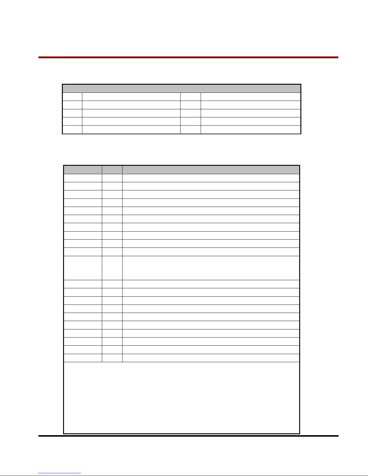
SMART Command Set
SMART Command Set
SMART Feature Register Values
D0h Read Data D5h Read Log
D1h Read Attribute Threshold D6h Write Log
D2h Enable/Disable Autosave D8h Enable SMART Operations
D3h Save Attribute Values D9h Disable SMART Operations
D4h Execute OFF-LINE Immediate DAh Return Status
1. If reserved size is below the Threshold, the status can be read from Cylinder register by Return Status command
(DAh).
SMART Data Structure
BYTE F / V
Decription
0-1 X Revision code
2-114 X Vendor specific
115-116 V Power cycle count (116=MSB, 115=LSB)
117-361 X Vendor specific
362 V Off line data collection status
363 X Self-test execution status byte
364-365 V Total time in seconds to complete off-line data collection activity
366 X Vendor specific
367 F Off-line data collection capability
368-369 F SMART capability
370 F
Error logging capability
7-1 Reserved
0 1=Device error logging supported
371 X Vendor specific
372 F Short self-test routine recommended polling time (in minutes)
373 F Extended self-test routine recommended polling time (in minutes)
374 F Conveyance self-test routine recommended polling time (in minutes)
375-385 R Reserved
386-395 F Firmware Version/Date Code
396-397 F Number of initial invalid block(396=MSB, 397=LSB)
398-399 V Number of run time bad block(398=MSB, 399=LSB)
400 V Number of spare block
511 V Data structure checksum
F=the content of the byte is fixed and does not change.
V=the content of the byte is variable and may change depending on the state of the device or
the commands executed by the device.
X=the content of the byte is vendor specific and may be fixed or variable.
R=the content of the byte is reserved and shall be zero.
* 4 Byte value : [MSB] [2] [1] [LSB]
Page 28
T
T
T
S
S
S
6
6
6
4
4
4
G
G
G
S
S
S
S
S
S
D
D
D
1
1
1
0
0
0
-
-
-
M
M
M
1.0” Solid State Disk
Transcend Information Inc.
V1.6
33
SMART Error Log.
ECC fail format:(Log address 0xA0h)
1 Byte
1 Byte 2 Byte 4 Byte
Count ECC fail Error Code Flash Block Address
LBA address
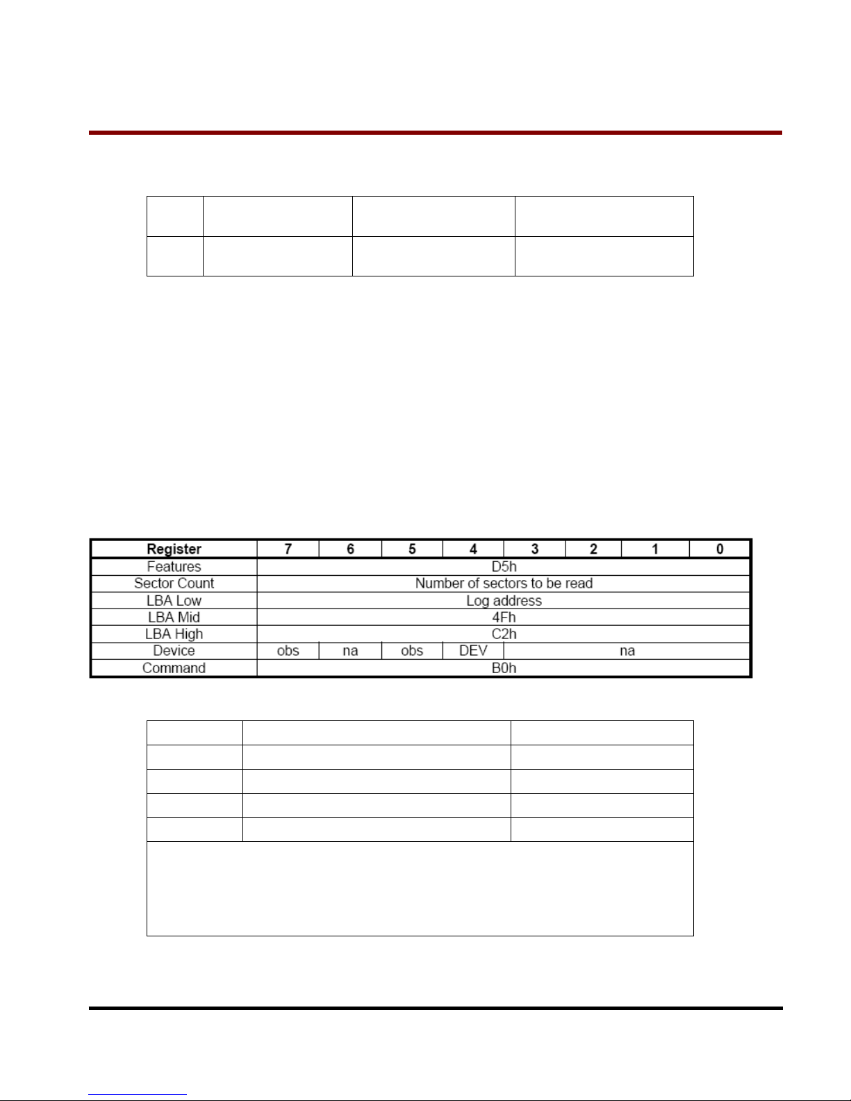
SMART Read Log
Command Code
B0h with the content of the Features register equal to D5h.
Input
The Features register shall be set to D5h.
The Sector Count register shall specify the number of sectors to be read from the log number
specified by the LBA Low register. It should specify 4. It can record 256 new bad blocks
information in this.
The LBA Mid register shall be set to 4Fh.
The LBA High register shall be set to C2h.
Log address definition
Log Address Content R/W
00h Log directory RO
01h Summary SMART error log RO
06h SMART self-test log RO
A0h Device vendor specific VS
Note:
RO - Log is read only by the host.
R/W - Log is read or written by the host.
VS - Log is vendor specific thus read/write abiltiy is vendor specific.
Page 29
T
T
T
S
S
S
6
6
6
4
4
4
G
G
G
S
S
S
S
S
S
D
D
D
1
1
1
0
0
0
-
-
-
M
M
M
1.0” Solid State Disk
Transcend Information Inc.
V1.6
34
Identify Device – ECh
Bit ->
7 6 5 4 3 2 1 0
Command (7)
ECh
C/D/H (6)
X X X Drive
X
Cyl High (5)
X
Cyl Low (4)
X
Sec Num (3)
X
Sec Cnt (2)
X
Feature (1)
X
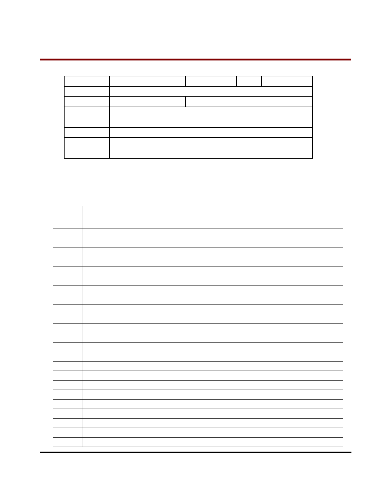
The Identify Device command enables the host to receive parameter information from the 1” SSD. This
command has the same protocol as the Read Sector(s) command. The parameter words in the buffer have
the arrangement and meanings defined in Table as below. All reserved bits or words are zero. Hosts should
not depend on Obsolete words in Identify Device containing 0. Table 47 specifies each field in the data
returned by the Identify Device Command. In Table as below, X indicates a numeric nibble value specific to
the card and aaaa indicates an ASCII string specific to the particular drive.
Word
Address
Default
Value
Total
Bytes
Data Field Type Information
0 044Ah 2 General configuration bit Significant
1 3FFFh 2 (16383) Default number of cylinders
2 0000h 2 Reserved
3 000Fh 2 (15) Default number of heads
4 0000h 2 Obsolete
5 0240h 2 Obsolete
6 003Fh 2 (63) Default number of sectors per track
7-8 07744000h 4 Number of sectors per card (Word 7 = MSW, Word 8 = LSW)
9 0000h 2 Obsolete
10-19 S/N 20 Serial number in ASCII (Right Justified)
20 0002h 2 Obsolete
21 0002h 2 Obsolete
22 0000h 2 Number of ECC bytes passed on Read/Write Long Commands
23-26 20091009 8 Firmware revision in ASCII. Big Endian Byte Order in Word
27-46 TS64GSSD10-M 40 Model number in ASCII (Left Justified) Big Endian Byte Order in Word
47 8001h 2 Maximum number of sectors on Read/Write Multiple command
48 0000h 2 Reserved
49 0F00h 2 Capabilities
50 0000h 2 Reserved
51 0200h 2 PIO data transfer cycle timing mode
52 0000h 2 Obsolete
53 0007h 2 Field Validity
54 3FFFh 2 (16383) Current numbers of cylinders
55 000Fh 2 (15) Current numbers of heads
Page 30
T
T
T
S
S
S
6
6
6
4
4
4
G
G
G
S
S
S
S
S
S
D
D
D
1
1
1
0
0
0
-
-
-
M
M
M
1.0” Solid State Disk
Transcend Information Inc.
V1.6
35
Word
Address
Default
Value
Total
Bytes
Data Field Type Information
56 0003Fh 2 (63) Current sectors per track
57-58 00EC3C4Fh 4 Current capacity in sectors (LBAs)(Word 57 = LSW, W ord 58 = MSW)
59 010xh 2 Multiple sector setting
60-61 07744000h 4 Total number of sectors addressable in LBA Mode
62 0000h 2 Reserved
63 0X07h 2 Multiword DMA transfer: Support MDMA Mode 0~2
64 0003h 2 Advanced PIO modes supported (Support PIO Mode 3 , 4)
65 0078h 2 (120ns) Minimum Multiword DMA transfer cycle time per word.
66 0078h 2 (120ns) Recommended Multiword DMA transfer cycle time.
67 0078h 2 (120ns) Minimum PIO transfer cycle time without flow control
68 0078h 2 (120ns) Minimum PIO transfer cycle time with DSTROBE flow control
69-75 0000h 14 Reserved
76 0000h 2
Reserve for SATA Capabilities (SATA interface=0006h, IDE
interface=0000h)
77-79 0000h 6 Reserved
80 0080h 2 Support ATA/ATAP1-7
81 0000h 2 Minor version numner
82 742Bh 2 Features/command sets supported
83 5100h 2 Features/command sets supported
84 4003h 2 Features/command sets supported
85 xxxxh 2 Features/command sets enabled
86 xxxxh 2 Features/command sets enabled
87 xxxxh 2 Features/command sets enabled
88 0x3Fh 2 Ultra DMA Mode Supported and Selected
89 0001h 2 Time required for Security erase unit completion
90 0000h 2 Time required for Enhanced security erase unit completion
91 0000h 2 Current Advanced power management value
92 FFFEh 2 Mater Password Revision Code
93 604Fh 2 Hardware reset result
94-127 0000h 68 Reserved
128 0001h 2 Security status
129-159
0000h 62 Vendor unique bytes
160 0000h 2 CFA Power mode
161 0000h 2 Reserved for assignment by the CFA
162 0000h 2 Key management schemes supported
163 0000h 2 CF Advanced True IDE Timing Mode Capability and Setting
164 0000h 2 CF Advanced PC Card I/O and Memory Timing Mode Capability
Page 31

T
T
T
S
S
S
6
6
6
4
4
4
G
G
G
S
S
S
S
S
S
D
D
D
1
1
1
0
0
0
-
-
-
M
M
M
1.0” Solid State Disk
Transcend Information Inc.
V1.6
36
165-175
0000h 22 Reserved
176-255
0000h 140 Reserved
 Loading...