

Transcend TS512MDOM44H-S, TS2GDOM44H, TS128MDOM44H, TS256MDOM44H-S, TS256MDOM44H DATASHEET
...Page 1
T
r
a
n
s
c
e
n
d
4
4
-
P
i
n
I
D
E
F
l
~
~
a
F
l
a
F
l
a
8
G
8
G
8
G
T
r
a
n
s
c
e
n
d
4
4
-
P
i
n
I
D
8
8
8
M
I
D
M
M
E
E
~
T
r
a
n
s
c
e
n
d
4
4
-
P
i
n
T
S
1
T
S
S
1
1
2
2
2
T
Description
Description
DescriptionDescription
With an IDE interface and strong data retention ability,
44-Pin IDE Flash Modules are ideal for use in the
harsh environments where Industrial PCs, Set-Top
Boxes, etc. are used.
Placement
Placement
PlacementPlacement
s
s
s
D
D
D
h
h
h
O
O
O
M
M
M
M
M
M
o
d
u
l
e
(
H
o
r
i
z
o
n
t
a
l
o
d
u
l
e
(
H
o
r
i
z
o
o
d
u
l
e
(
H
o
r
4
4
H
-
S
4
4
4
4
H
-
S
H
-
S
Features
Features
FeaturesFeatures
•
RoHS compliant products
•
Storage Capacity: 128MB ~ 8GB
• Operating Voltage: 3.3V ±5% or 5V ±10%
• Operating Temperature: 0°C ~ 70°C
• Operating Humidity (Non condensation): 0% to 95%
•
Storage Humidity (Non condensation): 0% to 95%
•
Endurance: 2,000,000 Program/Erase cycles
•
MTBF: 1,000,000 hours
•
Durability of Connector: 10,000 times
• Fully compatible with devices and OS that support the
IDE standard (pitch = 2.00mm)
•
Built-in ECC function assures high reliability of data
transfer
•
Supports up to Ultra DMA Mode 4
•
Supports PIO Mode 6
n
i
z
o
n
)
t
a
l
)
t
a
l
)
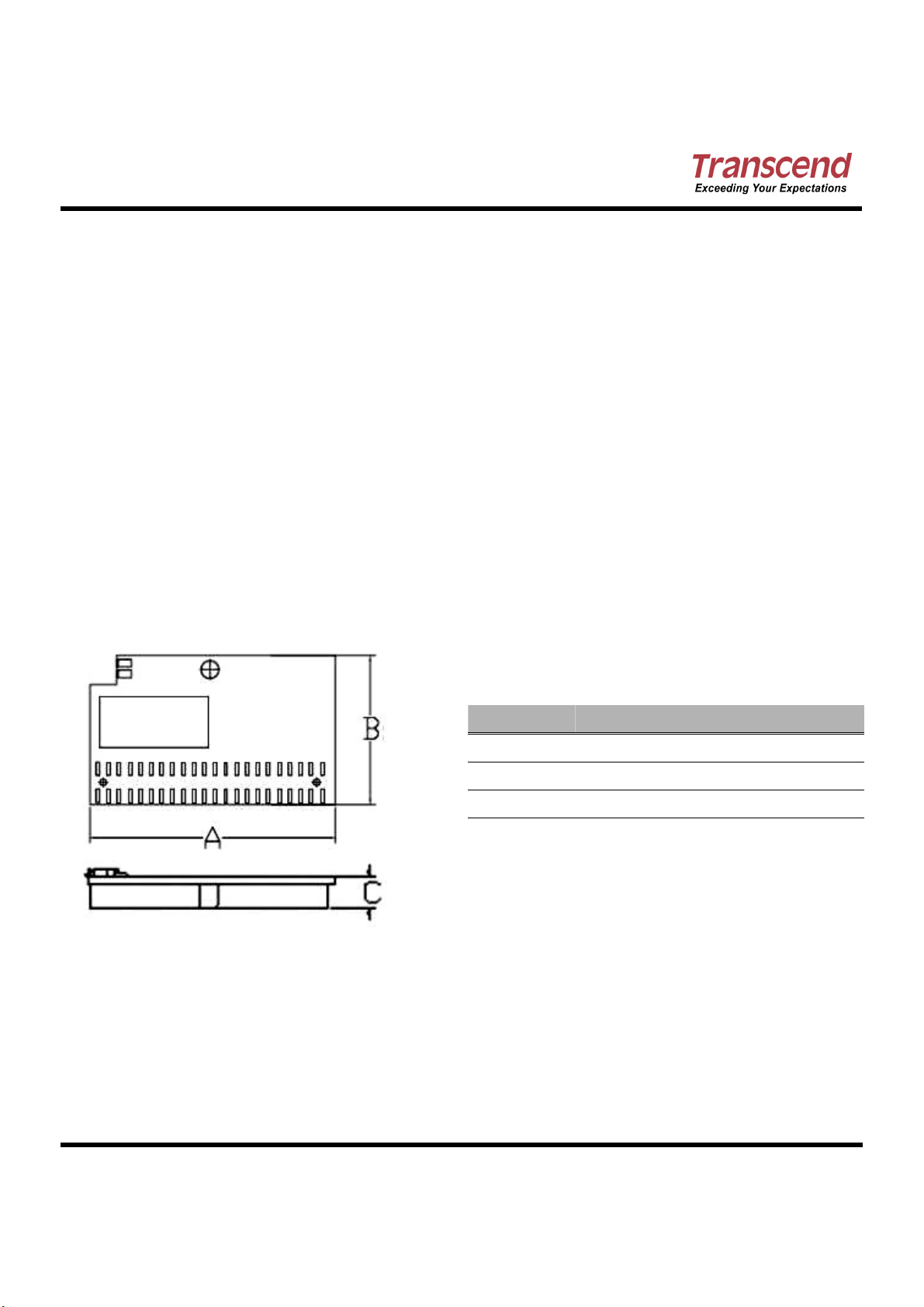
Dimensions
Dimensions
DimensionsDimensions
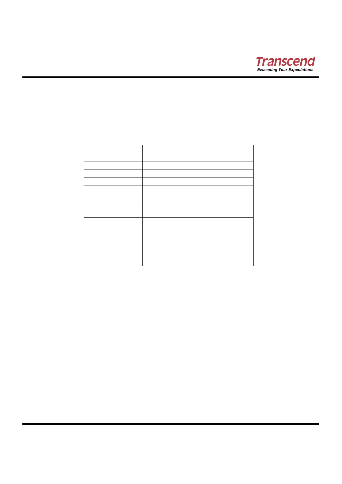
Side Millimeters Inches
A
B
C
46.00 ± 0.40 1.81 ± 0.016
28.00 ± 0.20 1.10 ± 0.008
6.00 ± 0.50 0.24 ± 0.020
Transcend Information Inc.
1
Ver 1.0
Page 2
T
Pin
Pin
r
a
n
s
c
e
n
d
4
4
-
P
i
n
I
D
E
F
l
a
T
r
a
n
s
c
e
n
d
4
4
-
P
i
n
I
D
8
8
8
M
I
M
M
E
D
E
~
~
Pin
Name
~
T
r
a
n
s
c
e
n
d
4
4
-
P
i
n
T
S
1
T
S
S
Pin
1
1
2
2
2
No
T
Pin
Pin Assignments
Assignments
Pin Pin
AssignmentsAssignments
Pin
No.
Name
01 -RESET 12 HD12 23 IOWB 34 PDIAGB
02 GND 13 HD2 24 GND 35 HA0
03 HD7 14 HD13 25 IORB 36 HA2
04 HD8 15 HD1 26 GND 37 CE1B
05 HD6 16 HD14 27 IORDY 38 CE2B
06 HD9 17 HD0 28 NC 39 DASPB
07 HD5 18 HD15 29 -DMACK 40 GND
08 HD10 19 GND 30 GND 41 VCC
09 HD4 20 NC 31 IREQ 42 VCC
10 HD11 21 DMARQ 32 IOIS16B 43 GND
11 HD3 22 GND 33 HA1 44 GND
Pin
No.
Name
s
F
l
a
s
F
l
a
s
8
G
D
8
G
D
8
G
D
Pin
No.
h
h
h
O
O
O
Pin
Name
M
M
M
M
M
M
o
o
o
4
4
4
d
u
l
e
(
H
o
r
i
z
o
n
t
a
l
d
u
l
e
(
H
o
r
i
z
o
d
u
l
e
(
H
o
r
4
H
-
S
4
4
H
-
S
H
-
S
Pin Definition
Pin Definition
Pin DefinitionPin Definition
Symbol Function
HD0 ~ HD15 Data Bus (Bi-directional)
HA0 ~ HA2 Address Bus (Input)
-RESET Device Reset (Input)
IORB Device I/O Read (Input)
IOWB Device I/O Write (Input)
IOIS16B Transfer Type 8/16 bit (Output)
CE1B, CE2B Chip Select (Input)
PDIAGB Pass Diagnostic (Bi-directional)
DASPB
DMARQ
DMACK-
IREQ Interrupt Request (Output)
NC No Connection
GND Ground
VCC Vcc Power Input
n
i
z
o
Disk Active/Slave Present
(Bi-directional)
DMA request
DMA acknowledge
n
)
t
a
l
)
t
a
l
)
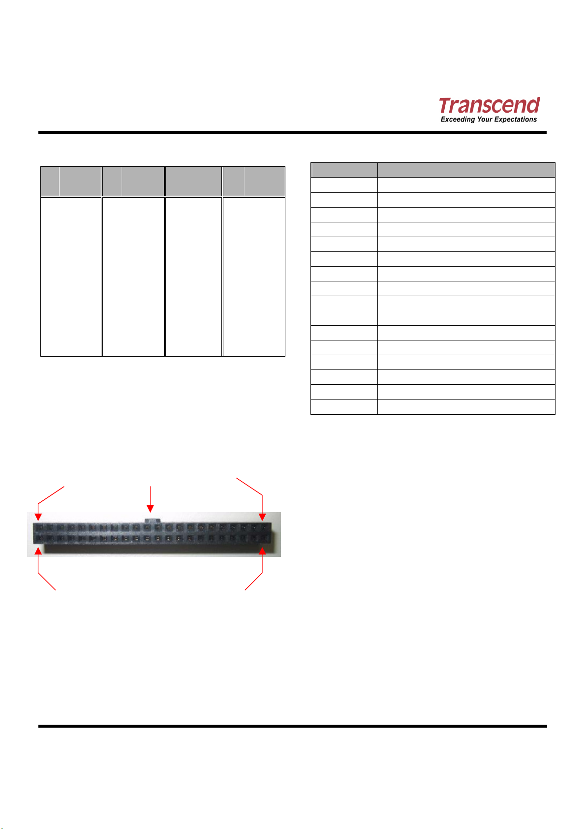
Pin
Pin Layout
Layout
Pin Pin
LayoutLayout
Pin1 Pin43
Pin2 Pin44
Bulge
Transcend Information Inc.
2
Ver 1.0
Page 3
T
r
a
n
s
c
e
T
r
a
n
T
r
a
n
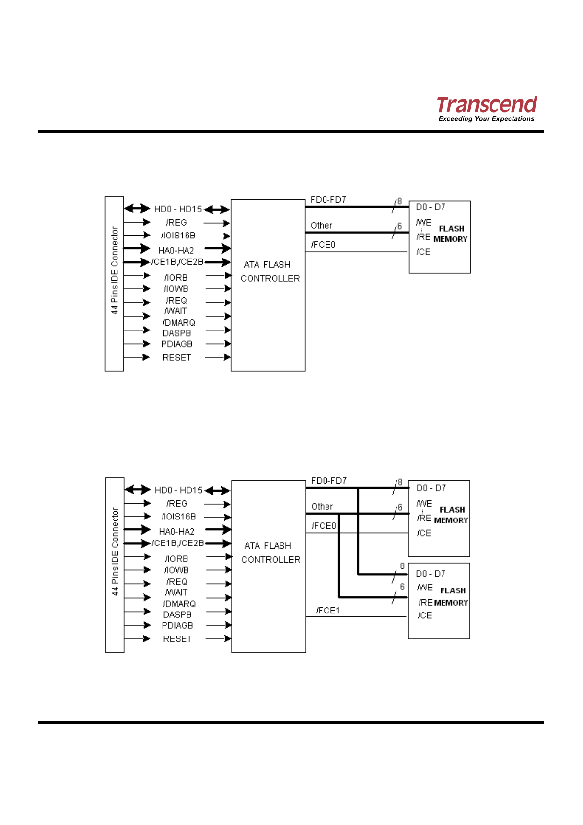
Block Diagram
Block Diagram
Block DiagramBlock Diagram
With 1 pcs of Flash Memory:
s
s
c
c
e
e
n
n
n
d
d
d
4
4
-
P
i
n
I
D
E
F
l
a
s
h
M
o
d
u
l
e
(
H
o
r
i
z
o
n
t
a
l
4
4
-
P
i
n
I
D
E
F
l
a
s
h
M
o
d
u
l
e
(
H
o
r
i
z
o
4
4
-
P
i
n
I
D
E
F
l
a
s
h
M
o
d
u
l
e
(
H
o
r
T
S
1
2
8
M
~
8
G
D
O
M
4
4
H
-
S
T
T
S
S
1
1
2
2
8
8
M
M
~
8
G
D
O
M
4
~
8
G
D
O
M
4
4
4
H
H
-
S
-
S
n
i
z
o
n
)
t
a
l
)
t
a
l
)
With 2 pcs of Flash Memory:
Transcend Information Inc.
3
Ver 1.0
Page 4
T
r
a
n
s
c
e
n
d
4
4
-
P
i
n
1
1
1
i
i
2
2
2
n
n
8
8
8
I
I
I
M
M
M
T
r
a
n
s
c
e
n
d
4
4
-
T
r
a
n
s
c
e
n
d
Absolute Maximum Rating
Absolute Maximum Ratingssss
Absolute Maximum RatingAbsolute Maximum Rating
Symbol Parameter Min Max Unit
VDD-VSS DC Power Supply -0.6 +6 V
P
4
4
-
P
T
S
T
S
T
S
D
D
D
E
E
E
~
~
~
F
l
a
s
h
M
o
d
u
l
e
(
H
o
r
i
z
o
n
t
a
l
F
l
a
s
h
M
o
d
u
l
e
(
H
o
r
i
z
o
F
l
a
s
h
M
o
d
u
l
e
(
H
o
r
8
G
D
O
M
4
4
H
-
S
8
G
D
O
M
4
8
G
D
O
M
4
4
4
H
H
-
S
-
S
n
i
z
o
n
)
t
a
l
)
t
a
l
)
Ta Operating Temperature 0 +70
Tst Storage Temperature -40 +85
Recommended Operating Conditions
Recommended Operating Conditions
Recommended Operating ConditionsRecommended Operating Conditions
Symbol Parameter Min Max Units
VDD Power supply 3.0 5.5 V
VIN Input voltage 0 VDD+0.3 V
Ta Operating Temperature 0 +70
DC Cha
DC Characteristics
DC ChaDC Cha
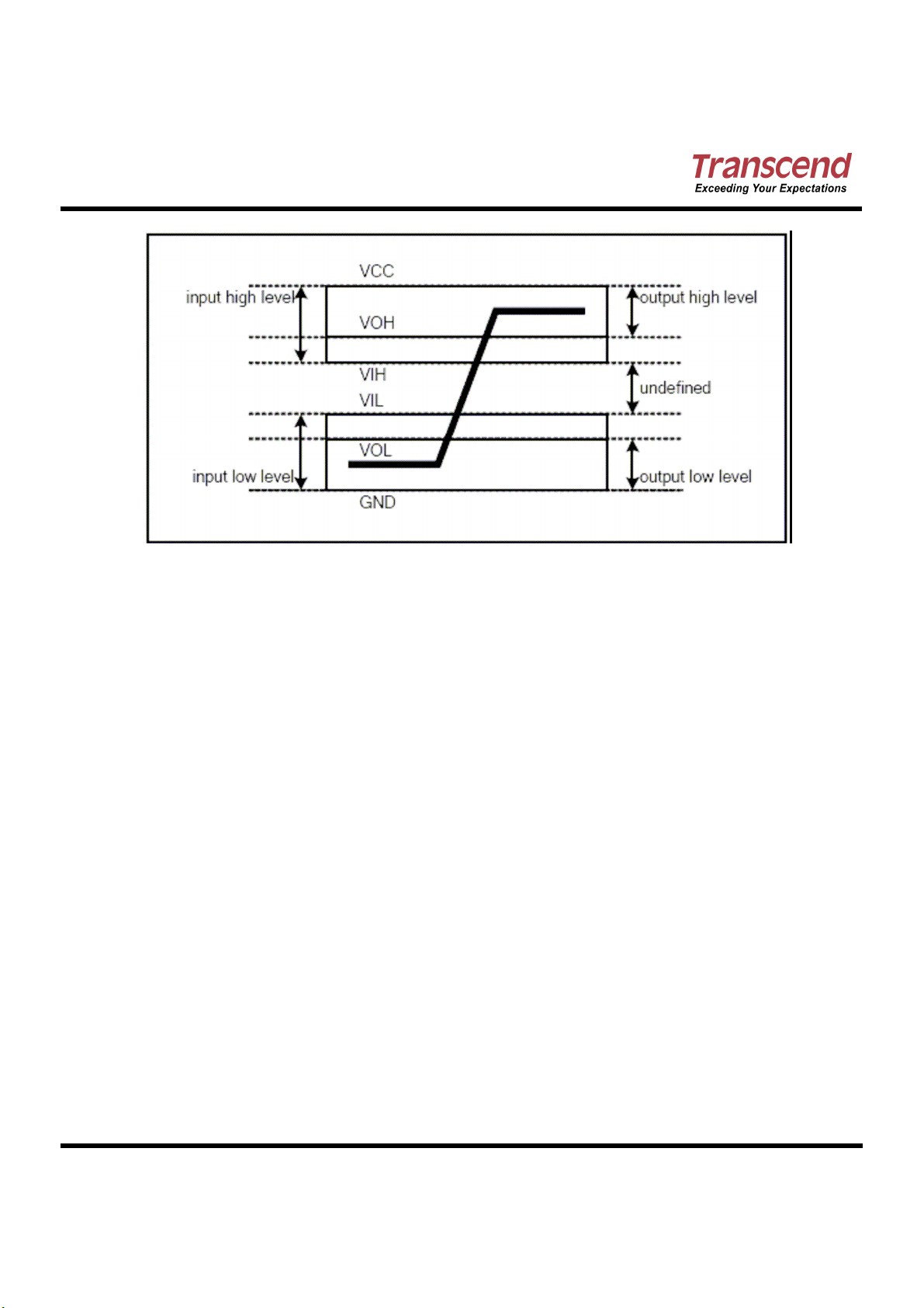
(Ta=0 oC to +70 oC, Vcc = 5.0V ±±±± 10%)
Supply Voltage VCC 4.5 5.5 V
High level output voltage VOH VCC-0.8 -- V
Low level output voltage VOL -- 0.8 V
High level input voltage
Low level input voltage
(Ta=0 oC to +70 oC, Vcc = 3.3V ±±±± 5%)
racteristics
racteristics racteristics
Parameter Symbol Min Max Unit Remark
VIH
VIL
4.0 --
2.92 --
-- 0.8
-- 1.70
V
Non-schmitt trigger
V
Schmitt trigger1
V
Non-schmitt trigger
V
Schmitt trigger1
°
C
°
C
°
C
Parameter Symbol Min Max Unit Remark
Supply Voltage VCC 3.135 3.465 V
High level output voltage VOH VCC-0.8 -- V
Low level output voltage VOL -- 0.8 V
High level input voltage
Low level input voltage
Transcend Information Inc.
VIH
VIL
2.4 --
2.05 --
-- 0.6
-- 1.25
4
V
Non-schmitt trigger
V
Schmitt trigger1
V
Non-schmitt trigger
V
Schmitt trigger1
Ver 1.0
Page 5
T
r
a
n
s
c
e
n
d
4
4
-
P
i
n
I
D
E
F
l
a
s
h
M
o
d
u
l
e
(
H
o
r
i
z
o
n
t
a
l
T
r
a
n
s
c
e
n
d
4
4
-
P
i
n
I
D
E
F
l
a
s
h
M
o
d
u
l
e
(
H
o
r
i
z
o
T
r
a
n
s
c
e
n
d
4
4
-
P
i
n
I
D
E
F
l
a
s
h
M
o
d
u
l
e
(
H
o
r
T
S
1
2
8
M
~
8
G
D
O
M
4
4
H
-
S
T
S
1
2
8
M
~
8
G
D
O
M
4
T
S
1
2
8
M
~
8
G
D
O
M
4
4
4
H
H
-
S
-
S
n
i
z
o
n
)
t
a
l
)
t
a
l
)
Transcend Information Inc.
5
Ver 1.0
Page 6
T
r
a
n
s
c
e
n
d
4
4
-
P
i
n
I
D
E
F
l
a
s
h
M
o
d
u
l
e
(
H
o
r
i
z
o
n
t
a
l
T
r
a
n
s
c
e
n
d
4
4
-
P
i
n
I
D
E
F
l
a
s
h
M
o
d
u
l
e
(
H
o
r
i
z
o
T
r
a
n
s
c
e
n
d
4
4
-
P
i
n
I
D
E
F
l
a
s
h
M
o
d
u
l
e
(
H
o
r
T
S
1
2
8
M
~
8
G
D
O
M
4
4
H
-
S
T
S
1
2
8
M
~
8
G
D
O
M
4
T
S
1
2
8
M
~
8
G
D
O
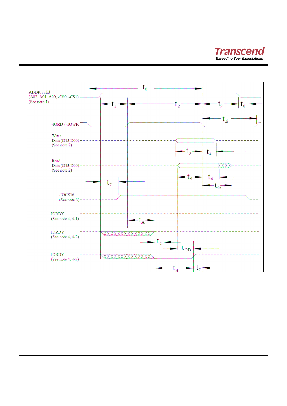
True IDE PIO Mode Read/Write Timing
t0
Cycle time (min) 1 600 383 240 180 120 100 80
t1
Address Valid to -IORD/-IOWR setup (min) 70 50 30 30 25 15 10
t2
-IORD/-IOWR (min) 1
t2
-IORD/-IOWR (min) Register (8 bit)
t2i
-IORD/-IOWR recovery time (min)
t3
-IOWR data setup (min)
t4
-IOWR data hold (min)
t5
-IORD data setup (min)
t6
-IORD data hold (min)
t
-IORD data tristate (max)2
6Z
t7
Address valid to IOCS16 assertion (max)
t8
Address valid to IOCS16 released (max)
t9
-IORD/-IOWR to address valid hold
Read Data Valid to IORDY active (min), if
t
RD
IORDY initially low after tA
tA
IORDY Setup time 3
tB
IORDY Pulse Width (max)
tC
IORDY assertion to release (max)
Notes: All timings are in nanoseconds. The maximum load on -IOCS16 is 1 LSTTL with a 50 pF (40pF below
120nsec Cycle Time) total load. All times are in nanoseconds. Minimum time from -IORDY high to -IORD
high is 0 nsec, but minimum -IORD width shall still be met.
Item
4
M
4
4
Mode
0
165 125 100 80 70 65 55
290 290 290 80 70 65 55
-- -- -- 70 25 25 20
60 45 30 30 20 20 15
30 20 15 10 10 5 5
50 35 20 20 20 15 10
5 5 5 5 5 5 5
30 30 30 30 30 20 20
4
90 50 40 N/A N/A N/A N/A
4
60 45 30 N/A N/A N/A N/A
20 15 10 10 10 10 10
0 0 0 0 0 0 0
35 35 35 35 35 N/A
1250 1250 1250 1250 1250 N/A
5 5 5 5 5 N/A
H
H
-
S
-
S
Mode
1
i
z
o
Mode
2
n
n
t
a
l
t
a
Mode
3
)
)
l
)
Mode
4
Mode
5
5
5
5
Mode
6
N/A
N/A
N/A
5
5
5
(1) t0 is the minimum total cycle time, t2 is the minimum command active time, and t2i is the minimum
command recovery time or command inactive time. The actual cycle time equals the sum of the actual
command active time and the actual command inactive time. The three timing requirements of t0, t2, and
t
shall be met. The minimum total cycle time requirement is greater than the sum of t2 and t2i. This means
2i
a host implementation can lengthen either or both t2 or t2i to ensure that t0 is equal to or greater than the
value reported in the device’s identify device data.
(2) This parameter specifies the time from the negation edge of -IORD to the time that the data bus is
released by the device.
(3) The delay from the activation of -IORD or -IOWR until the state of IORDY is first sampled. If IORDY is
inactive then the host shall wait until IORDY is active before the PIO cycle can be completed. If the device
is not driving IORDY negated at tA after the activation of -IORD or -IOWR, then t5 shall be met and tRD is
not applicable. If the device is driving IORDY negated at the time tA after the activation of -IORD or -IOWR,
then tRD shall be met and t5 is not applicable.
(4) t7 and t8 apply only to modes 0, 1 and 2. For other modes, this signal is not valid.
(5) IORDY is not supported in this mode.
Transcend Information Inc.
6
Ver 1.0
Page 7
T
r
a
n
s
c
e
n
d
4
4
-
P
i
n
I
D
E
F
l
~
~
a
F
l
a
F
l
a
8
G
8
G
8
G
T
r
a
n
s
c
e
n
d
4
4
-
P
i
n
I
D
8
8
8
M
I
D
M
M
E
E
~
T
r
a
n
s
c
e
n
d
4
4
-
P
i
n
T
S
1
T
S
S
1
1
2
2
2
T
True IDE PIO Mode Timing Diagram
s
s
s
D
D
D
h
h
h
O
O
O
M
M
M
M
M
M
o
o
o
4
4
4
d
4
4
d
d
4
u
u
u
H
H
H
l
e
(
H
o
r
i
z
o
n
t
a
l
l
e
(
H
o
r
i
z
o
l
e
(
H
o
r
-
S
-
S
-
S
n
i
z
o
n
)
t
a
l
)
t
a
l
)
Figure 1: True IDE PIO Mode Timing Diagram
Notes:
(1) Device address consists of -CS0, -CS1, and A[02::00]
(2) Data consists of D[15::00] (16-bit) or D[07::00] (8 bit)
(3) -IOCS16 is shown for PIO modes 0, 1 and 2. For other modes, this signal is ignored.
(4) The negation of IORDY by the device is used to extend the PIO cycle. The determination of whether the cycle
is to be extended is made by the host after tA from the assertion of -IORD or -IOWR. The assertion and
negation of IORDY is described in the following three cases:
(4-1) Device never negates IORDY: No wait is generated.
(4-2) Device starts to drive IORDY low before tA, but causes IORDY to be asserted before tA: No wait
generated.
(4-3) Device drives IORDY low before tA: wait generated. The cycle completes after IORDY is reasserted. For
cycles where a wait is generated and -IORD is asserted, the device shall place read data on D15-D00 for
tRD before causing IORDY to be asserted.
Transcend Information Inc.
7
Ver 1.0
Page 8

T
r
a
n
s
c
e
n
d
4
4
-
P
i
n
I
D
E
F
l
a
s
h
M
o
d
u
l
e
(
H
o
r
i
z
o
n
t
a
l
T
r
a
n
s
c
e
n
d
4
4
-
P
i
n
I
D
E
F
l
a
s
h
M
o
d
u
l
e
(
H
o
r
i
z
o
T
r
a
n
s
c
e
n
d
4
4
-
P
i
n
I
D
E
F
l
a
s
h
M
o
d
u
l
e
(
H
o
r
T
S
1
2
8
M
~
8
G
D
O
M
4
4
H
-
S
T
S
1
2
8
M
~
8
G
D
O
M
4
T
S
1
2
8
M
~
8
G
D
O
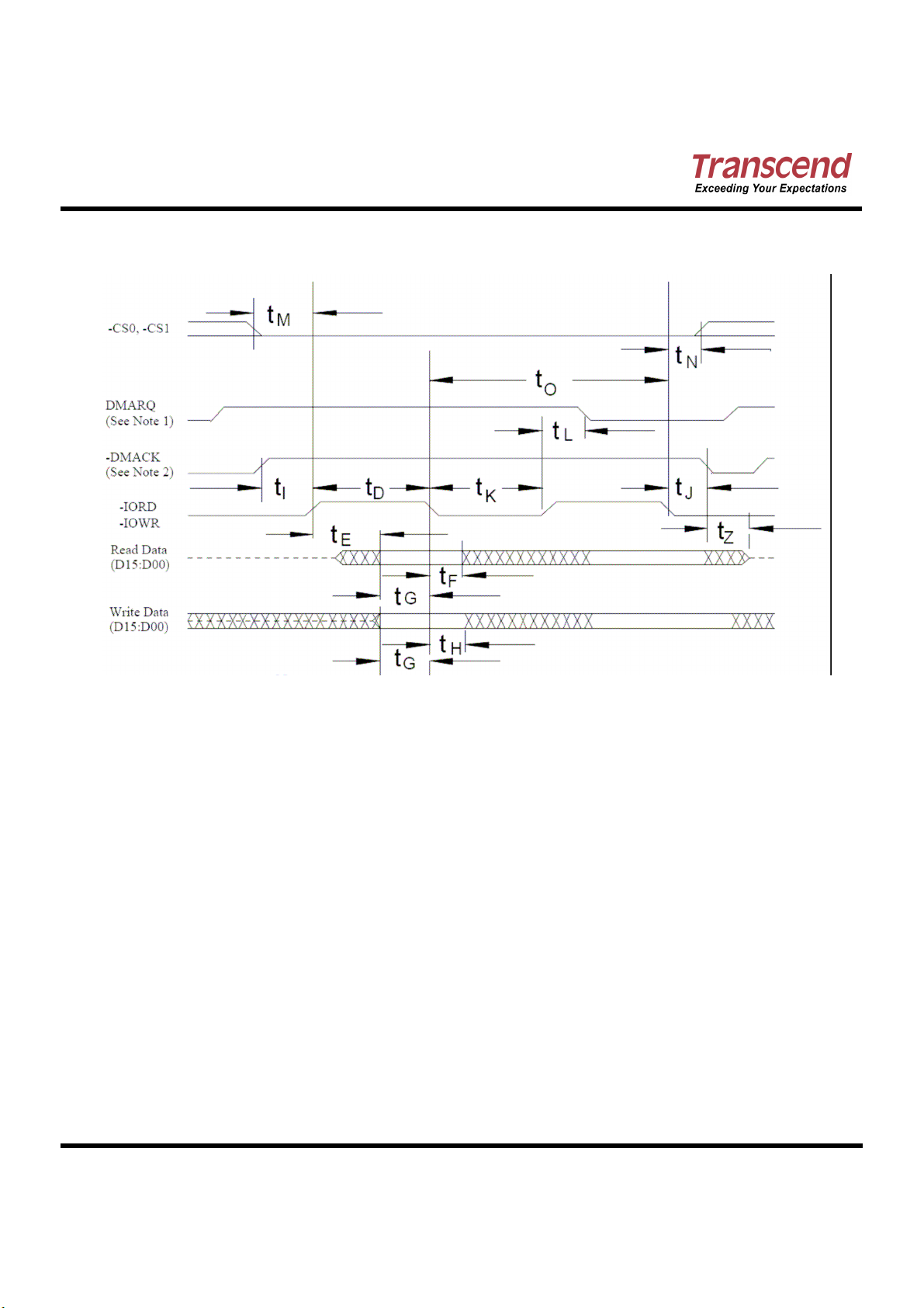
True IDE Multiword DMA Mode Read/Write Timing Specification
M
4
4
4
H
H
-
S
-
S
n
i
z
o
n
)
t
a
l
)
t
a
l
)
t0
Cycle time (min) 1 480 150 120 100 80
tD
-IORD / -IOWR asserted width(min)
tE
-IORD data access (max) 150 60 50 50 45
tF
-IORD data hold (min) 5 5 5 5 5
tG
-IORD/-IOWR data setup (min) 100 30 20 15 10
tH
-IOWR data hold (min) 20 15 10 5 5
DMACK to –IORD/-IOWR setup
tI
(min)
-IORD / -IOWR to -DMACK hold
tJ
(min)
t
-IORD negated width (min) 1 50 50 25 25 20
KR
t
-IOWR negated width (min) 1 215 50 25 25 20
KW
t
-IORD to DMARQ delay (max) 120 40 35 35 35
LR
t
-IOWR to DMARQ delay (max) 40 40 35 35 35
LW
tM
CS(1:0) valid to –IORD / -IOWR 50 30 25 10 5
tN
CS(1:0) hold 15 10 10 10 10
tZ
-DMACK 20 25 25 25 25
Item
Mode 0
(ns)
1
215 80 70 65 55
0 0 0 0 0
20 5 5 5 5
Mode 1
(ns)
Mode 2
(ns)
Mode 3
(ns)
Mode 4
(ns)
Notes:
(1) t0 is the minimum total cycle time and tD is the minimum command active time, while tKR and tKW are the
minimum command recovery time or command inactive time for input and output cycles respectively. The
actual cycle time equals the sum of the actual command active time and the actual command inactive
time. The three timing requirements of t0, tD, tKR, and tKW shall be met. The minimum total cycle time
requirement is greater than the sum of tD and tKR or tKW.for input and output cycles respectively. This
means a host implementation can lengthen either or both of tD and either of tKR, and tKW as needed to
ensure that t0 is equal to or greater than the value reported in the device’s identify device data.
Transcend Information Inc.
8
Ver 1.0
Page 9
T
r
a
n
s
c
e
n
d
4
4
-
P
i
n
I
D
E
F
l
a
s
h
M
o
d
u
l
e
(
H
o
r
i
z
o
n
T
r
a
n
s
c
e
n
d
4
4
-
P
i
n
I
D
E
F
l
a
s
h
M
o
d
u
l
e
(
H
o
r
T
r
a
n
s
c
e
n
d
4
4
-
P
i
n
I
D
E
F
l
a
s
h
M
o
d
u
l
e
(
T
S
1
2
8
M
~
8
G
D
O
M
4
4
H
-
S
T
S
1
2
8
M
~
8
G
D
O
M
4
T
S
1
2
8
M
~
8
G
D
O
True IDE Multiword DMA Mode Read/Write Timing Diagram
M
4
4
4
H
H
-
S
-
S
H
o
i
r
i
z
z
o
o
n
n
t
a
l
)
t
a
l
)
t
a
l
)
Figure 2: True IDE Multiword DMA Mode Read/Write Timing Diagram
Notes:
(1) If the Card cannot sustain continuous, minimum cycle time DMA transfers, it may negate DMARQ within the
time specified from the start of a DMA transfer cycle to suspend the DMA transfers in progress and reassert
the signal at a later time to continue the DMA operation.
(2) This signal may be negated by the host to suspend the DMA transfer in progress.
Transcend Information Inc.
9
Ver 1.0
Page 10
T
r
a
n
s
c
e
n
d
4
4
-
P
i
n
I
D
E
F
l
a
s
h
M
o
d
u
l
e
(
H
o
r
i
z
o
n
t
a
l
T
r
a
n
s
c
e
n
d
4
4
-
P
i
n
I
D
E
F
l
a
s
h
M
o
d
u
l
e
(
H
o
r
i
z
o
T
r
a
n
s
c
e
n
d
4
4
-
P
i
n
I
D
E
F
l
a
s
h
M
o
d
u
l
e
(
H
o
r
T
S
1
2
8
M
~
8
G
D
O
M
4
4
H
-
S
T
S
1
2
8
M
~
8
G
D
O
M
4
T
S
1
2
8
M
~
8
G
D
O
Ultra DMA Mode Read/Write Timing Specification
Ultra DMA is an optional data transfer protocol used with the READ DMA, and WRITE DMA,
commands. When this protocol is enabled, the Ultra DMA protocol shall be used instead of the Multiword
DMA protocol when these commands are issued by the host. This protocol applies to the Ultra DMA data
burst only. When this protocol is used there are no changes to other elements of the ATA protocol.
UDMA Signal Type
DMARQ Output DMARQ
DMACK Input -DMACK
STOP Input STOP1
HDMARDY(R)
HSTROBE(W)
DDMARDY(W)
DSTROBE(R)
DATA Bidir D[15:00]
ADDRESS Input A[02:00]5
CSEL input -CSEL
INTRQ Output INTRQ
Card Select Input
M
4
Input
Output
4
4
H
H
-
S
-
S
TRUE IDE MODE
-HDMARDY
HSTROBE(W)
-DDMARDY(W)
DSTROBE(R)
i
z
o
UDMA
-CS0
-CS1
n
n
)
t
a
l
)
t
a
l
)
1,2
1,3,4
1,3
1,2,4
Notes: 1) The UDMA interpretation of this signal is valid only during an Ultra DMA data burst.
2) The UDMA interpretation of this signal is valid only during and Ultra DMA data burst during a DMA Read command.
3) The UDMA interpretation of this signal is valid only during an Ultra DMA data burst during a DMA Write command.
4) The HSTROBE and DSTROBE signals are active on both the rising and the falling edge.
5) Address lines 03 through 10 are not used in True IDE mode.
Several signal lines are redefined to provide different functions during an Ultra DMA data burst.
These lines assume their UDMA definitions when:
1. An Ultra DMA mode is selected, and
2. A host issues a READ DMA, or a WRITE DMA command requiring data transfer, and
3. The device asserts (-)DMARQ, and
4. The host asserts (-)DMACK.
These signal lines revert back to the definitions used for non-Ultra DMA transfers upon the negation
of -DMACK by the host at the termination of an Ultra DMA data burst.
With the Ultra DMA protocol, the STROBE signal that latches data from D[15:00] is generated by the
same agent (either host or device) that drives the data onto the bus. Ownership of D[15:00] and this data
strobe signal are given either to the device during an Ultra DMA data-in burst or to the host for an Ultra
Transcend Information Inc.
10
Ver 1.0
Page 11

T
r
a
n
s
c
e
n
d
4
4
-
P
i
n
I
D
E
F
l
a
s
h
M
o
d
u
l
e
(
H
o
r
i
z
o
n
t
a
l
T
r
a
n
s
c
e
n
d
4
4
-
P
i
n
I
D
E
F
l
a
s
h
M
o
d
u
l
e
(
H
o
r
i
z
o
T
r
a
n
s
c
e
n
d
4
4
-
P
i
n
I
D
E
F
l
a
s
h
M
o
d
u
l
e
(
H
o
r
T
S
1
2
8
M
~
8
G
D
O
M
4
4
H
-
S
T
S
1
2
8
M
~
8
G
D
O
M
4
T
S
1
2
8
M
~
8
G
D
O
DMA data-out burst.
During an Ultra DMA data burst a sender shall always drive data onto the bus, and, after a sufficient
time to allow for propagation delay, cable settling, and setup time, the sender shall generate a STROBE
edge to latch the data. Both edges of STROBE are used for data transfers so that the frequency of
STROBE is limited to the same frequency as the data.
Words in the IDENTIFY DEVICE data indicate support of the Ultra DMA feature and the Ultra DMA
modes the device is capable of supporting. The Set transfer mode subcommand in the SET FEATURES
command shall be used by a host to select the Ultra DMA mode at which the system operates. The Ultra
DMA mode selected by a host shall be less than or equal to the fastest mode of which the device is
capable. Only one Ultra DMA mode shall be selected at any given time. All timing requirements for a
selected Ultra DMA mode shall be satisfied. Devices supporting any Ultra DMA mode shall also support
all slower Ultra DMA modes.
An Ultra DMA capable device shall retain the previously selected Ultra DMA mode after executing a
software reset sequence or the sequence caused by receipt of a DEVICE RESET command if a SET
FEATURES disable reverting to defaults command has been issued. The device may revert to a
Multiword DMA mode if a SET FEATURES enable reverting to default has been issued. An Ultra DMA
capable device shall clear any previously selected Ultra DMA mode and revert to the default non-Ultra
DMA modes after executing a power-on or hardware reset.
M
4
4
4
H
H
-
S
-
S
n
i
z
o
n
)
t
a
l
)
t
a
l
)
Both the host and device perform a CRC function during an Ultra DMA data burst. At the end of an
Ultra DMA data burst the host sends its CRC data to the device. The device compares its CRC data to the
data sent from the host. If the two values do not match, the device reports an error in the error register. If
an error occurs during one or more Ultra DMA data bursts for any one command, the device shall report
the first error that occurred. If the device detects that a CRC error has occurred before data transfer for
the command is complete, the device may complete the transfer and report the error or abort the
command and report the error.
NOTE
through to the host software driver regardless of whether all data requested by the command has been
transferred.
−
If a data transfer is terminated before completion, the assertion of INTRQ should be passed
Transcend Information Inc.
11
Ver 1.0
Page 12

T
Measure location
r
a
n
s
c
e
n
d
4
4
-
P
i
n
I
D
E
F
l
a
s
h
M
T
r
a
n
s
c
e
n
d
4
4
-
P
i
n
I
D
E
F
l
a
T
r
a
n
s
c
e
n
d
4
4
-
P
i
n
I
D
E
T
S
1
2
8
M
~
T
S
1
2
S
1
2
8
8
T
Ultra DMA Data Burst Timing Requirements
M
M
~
~
s
F
l
a
s
8
G
D
8
G
D
8
G
D
h
h
O
O
O
M
M
M
M
M
o
o
4
4
o
4
d
4
4
d
d
4
u
u
u
H
H
H
l
e
(
H
o
r
i
z
o
n
t
a
l
l
e
(
H
o
r
i
z
o
l
e
(
H
o
r
-
S
-
S
-
S
n
i
z
o
n
)
t
a
l
)
t
a
l
)
Name
t
2CYCTYP
t
112 73 54 39 25 Note 3
CYC
t
230 153
2CYC
tDS 15.0 10.0
tDH 5.0 5.0 5.0 5.0 5.0 Recipient
t
70.0 48.0
DVS
t
6.2 6.2 6.2 6.2 6.2 Sender
DVH
tCS 15.0 10.0
tCH 5.0 5.0 5.0 5.0 5.0 Device
t
70.0 48.0
CVS
t
6.2 6.2 6.2 6.2 6.2 Host
CVH
t
0 0 0 0 0 Device
ZFS
t
70.0 48.0
DZFS
tFS 230 200 170 130 120 Device
tLI 0 150 0 150 0 150 0 100 0 100 Note 4
t
20 20 20 20 20 Host
MLI
tUI 0 0 0 0 0 Host
tAZ 10 10 10 10 10 Note 5
t
20 20 20 20 20 Host
ZAH
t
0 0 0 0 0 Device
ZAD
t
20 70 20 70 20 70 20 55 20 55 Host
ENV
t
75 70 60 60 60 Sender
RFS
tRP 160 125
t
IORDYZ
t
ZIORDY
t
20 20 20 20 20 Host
ACK
tSS 50 50 50 50 50 Sender
UDMA Mode 0 UDMA Mode 1 UDMA Mode 2 UDMA Mode 3 UDMA Mode 4
Min Max Min Max Min Max Min Max Min Max
240 160
20 20 20 20 20 Device
0 0 0 0 0 Device
120
115
7.0 7.0 5.0 Recipient
31.0
7.0 7.0 5.0 Device
31.0
31.0
100
90 60 Sender
86 57 Sender
20.0 6.7 Sender
20.0 6.7 Host
20.0 6.7 Sender
100 100 Recipient
(See Note 2)
Notes: All Timings in ns
(1) All timing measurement switching points (low to high and high to low) shall be taken at 1.5 V.
(2) All signal transitions for a timing parameter shall be measured at the connector specified in the measurement
location column. For example, in the case of t
sender connector.
(3) The parameter t
(4) The parameter t
incoming transition from the recipient or sender respectively. Both the incoming signal and the outgoing
response shall be measured at the same connector.
(5) The parameter tAZ shall be measured at the connector of the sender or recipient that is driving the bus but must
release the bus to allow for a bus turnaround.
(6) See Page 14 the AC Timing requirements in Ultra DMA AC Signal Requirements.
Transcend Information Inc.
shall be measured at the recipient’s connector farthest from the sender.
CYC
shall be measured at the connector of the sender or recipient that is responding to an
LI
, both STROBE and -DMARDY transitions are measured at the
RFS
12
Ver 1.0
Page 13

T
HDMARDY during data in burst initiation and
r
a
n
s
c
e
n
d
4
4
-
P
i
n
I
D
E
F
l
a
s
h
T
r
a
n
s
c
e
n
d
4
4
-
P
i
n
I
D
E
F
l
~
~
a
F
l
a
8
G
8
G
8
G
T
r
a
n
s
c
e
n
d
4
4
-
P
i
n
I
D
E
T
S
1
2
8
M
T
S
1
S
1
2
2
T
Ultra DMA Data Burst Timing Descriptions
8
8
M
M
~
s
s
D
D
D
h
h
O
O
O
M
M
M
M
M
M
o
o
o
4
4
4
d
4
4
d
d
4
u
u
u
H
H
H
l
e
(
H
o
r
i
z
o
n
t
a
l
l
e
(
H
o
r
i
z
o
l
e
(
H
o
r
-
S
-
S
-
S
n
i
z
o
n
)
t
a
l
)
t
a
l
)
Name
t
2CYCTYP
t
t
Notes:
(1) The parameters tUI, t
(2) 80-conductor cabling (see see ATA specification :Annex A)) shall be required in order to meet setup (tDS, tCS) and hold (tDH,
(3) Timing for
(4) For all timing modes the parameter t
Typical sustained average two cycle time
t
CYC
t
2CYC
tDS
tDH
t
DVS
t
DVH
tCS
tCH
t
CVS
t
CVH
t
ZFS
t
DZFS
tFS
tLI
t
MLI
tUI
tAZ
t
ZAH
t
ZAD
t
ENV
t
RFS
tRP
IORDYZ
ZIORDY
t
ACK
tSS
Burst Host Termination Timing), and tLI indicate sender-to-recipient or recipient-to-sender interlocks,i.e., one agent (either
sender or recipient) is waiting for the other agent to respond with a signal before proceeding.tUI is an unlimited interlock
that has no maximum time value. tMLI is a limited time-out that has a defined minimum. tLI is a limited time-out that has a
defined maximum.
tCH) times in modes greater than 2.
Data and STROBE signals have the same capacitive load value. Due to reflections on the cable, these timing
measurements are not valid in a normally functioning system.
Cycle time allowing for asymmetry and clock variations (from STROBE edge to STROBE
edge)
Two cycle time allowing for clock variations (from rising edge to next rising edge or from
falling edge to next falling edge of STROBE)
Data setup time at recipient (from data valid until STROBE edge)
Data hold time at recipient (from STROBE edge until data may become invalid)
Data valid setup time at sender (from data valid until STROBE edge)
Data valid hold time at sender (from STROBE edge until data may become invalid)
CRC word setup time at device
CRC word hold time device
CRC word valid setup time at host (from CRC valid until -DMACK negation)
CRC word valid hold time at sender (from -DMACK negation until CRC may become
invalid)
Time from STROBE output released-to-driving until the first transition of critical timing.
Time from data output released-to-driving until the first transition of critical timing.
First STROBE time (for device to first negate DSTROBE from STOP during a data in burst)
Limited interlock time
Interlock time with minimum
Unlimited interlock time
Maximum time allowed for output drivers to release (from asserted or negated)
Minimum delay time required for output
drivers to assert or negate (from released)
Envelope time (from -DMACK to STOP and -
from DMACK to STOP during data out burst initiation)
Ready-to-final-STROBE time (no STROBE edges shall be sent this long after negation of
-DMARDY)
Ready-to-pause time (that recipient shall wait to pause after negating -DMARDY)
Maximum time before releasing IORDY
Minimum time before driving IORDY
Setup and hold times for -DMACK (before assertion or negation)
Time from STROBE edge to negation of DMARQ or assertion of STOP (when sender
terminates a burst)
(in Page 19: Ultra DMA Data-In Burst Device Termination Timing and Page 20: Ultra DMA Data-In
MLI
t
,
t
, t
DVS
DVH
CVS
and t
shall be met for lumped capacitive loads of 15 and 40 pF at the connector where the
CVH
may be greater than t
ZIORDY
Comment Notes
2,
2,
3
3
2
2
3
3
1
1
1
4,
due to the fact that the host has a pull-up on IORDY-
ENV
Transcend Information Inc.
13
Ver 1.0
Page 14

T
r
a
n
s
c
e
n
d
4
4
-
P
i
n
I
D
E
F
l
a
s
h
M
o
d
u
l
e
(
H
o
T
r
a
n
s
c
e
n
d
4
4
-
P
i
n
I
D
E
F
l
a
s
h
M
o
d
u
l
e
T
r
a
n
s
c
e
n
d
4
4
-
P
i
n
I
D
E
F
l
a
s
h
M
o
d
T
S
1
2
8
M
~
8
G
D
O
M
4
T
S
1
2
8
M
~
8
G
D
T
S
1
2
8
M
~
8
giving it a known state when released.
Ultra DMA Sender and Recipient IC Timing Requirements
G
D
O
O
M
M
4
4
4
4
4
u
H
H
H
l
e
-
S
-
S
-
S
r
(
H
o
r
(
H
o
i
z
o
n
t
a
l
n
)
t
a
l
)
t
a
l
)
i
z
o
r
n
i
z
o
Name
t
DSIC
t
DHIC
t
DVSIC
t
DVHIC
t
DSIC
t
DHIC
t
DVSIC
t
DVHIC
Notes:
(1) All timing measurement switching points(low to high and high to low) shall be taken at 1.5 V.
(2) The correct data value shall be captured by the recipient given input data with a slew rate of 0.4 V/ns rising and
falling and the input STROBE with a slew rate of 0.4 V/ns rising and falling at t
measured through 1.5 V).
(3) The parameters t
signals have the same capacitive load value. Noise that may couple onto the output signals from external
sources has not been included in these values.
UDMA Mode 0 (ns) UDMA Mode 1 (ns) UDMA Mode 2 (ns) UDMA Mode 3 (ns) UDMA Mode 4 (ns)
Min Max Min Max Min Max Min Max Min Max
14.7 9.7 6.8 6.8 4.8
4.8 4.8 4.8 4.8 4.8
72.9 50.9 33.9 22.6 9.5
9.0 9.0 9.0 9.0 9.0
Recipient IC data setup time (from data valid until STROBE edge) (see note 2)
Recipient IC data hold time (from STROBE edge until data may become invalid) (see note 2)
Sender IC data valid setup time (from data valid until STROBE edge) (see note 3)
Sender IC data valid hold time (from STROBE edge until data may become invalid) (see note 3)
DVSIC
and t
and t
DSIC
shall be met for lumped capacitive loads of 15 and 40 pF at the IC where all
DVHIC
timing (as
DHIC
Ultra DMA AC Signal Requirements
Name Comment Min[V/ns] Max [V/ns] Note
S
RISE
S
FALL
Note:
(1) The sender shall be tested while driving an 18 inch long, 80 conductor cable with PVC insulation material. The
signal under test shall be cut at a test point so that it has not trace, cable or recipient loading after the test
point. All other signals should remain connected through to the recipient. The test point may be located at any
point between the sender’s series termination resistor and one half inch or less of conductor exiting the
connector. If the test point is on a cable conductor rather than the PCB, an adjacent ground conductor shall
also be cut within one half inch of the connector.
The test load and test points should then be soldered directly to the exposed source side connectors. The test
loads consist of a 15 pF or a 40 pF, 5%, 0.08 inch by 0.05 inch surface mount or smaller size capacitor from
the test point to ground. Slew rates shall be met for both capacitor values.
Measurements shall be taken at the test point using a <1 pF, >100 Kohm, 1 Ghz or faster probe and a 500
MHz or faster oscilloscope. The average rate shall be measured from 20% to 80% of the settled VOH level
with data transitions at least 120 nsec apart. The settled VOH level shall be measured as the average output
high level under the defined testing conditions from 100 nsec after 80% of a rising edge until 20% of the
Transcend Information Inc.
Rising Edge Slew Rate for any signal 1.25 1
Falling Edge Slew Rate for any signal 1.25 1
14
Ver 1.0
Page 15

T
r
a
n
s
c
e
n
d
T
r
a
n
s
c
n
s
c
e
T
r
a
subsequent falling edge.
e
n
n
d
d
4
4
-
P
i
n
I
D
E
F
l
a
s
h
M
o
d
u
l
e
(
H
o
r
i
z
o
n
t
a
l
4
4
-
P
i
n
I
D
E
F
l
a
s
h
M
o
d
u
l
e
(
H
o
r
i
z
o
4
4
-
P
i
n
I
D
E
F
l
a
s
h
M
o
d
u
l
e
(
H
o
r
T
S
1
2
8
M
~
8
G
D
O
M
4
4
H
-
S
T
T
S
S
1
1
2
2
8
8
M
M
~
8
G
D
O
M
4
~
8
G
D
O
M
4
4
4
H
H
-
S
-
S
n
i
z
o
n
)
t
a
l
)
t
a
l
)
Transcend Information Inc.
15
Ver 1.0
Page 16

T
r
a
n
s
c
e
n
d
4
4
-
P
i
n
I
D
E
F
l
a
s
h
M
o
d
u
l
e
(
H
o
r
i
z
o
n
t
a
l
T
r
a
n
s
c
e
n
d
4
4
-
P
i
n
I
D
E
F
l
a
s
h
M
o
d
u
l
e
(
H
o
r
i
z
o
T
r
a
n
s
c
e
n
d
4
4
-
P
i
n
I
D
E
F
l
a
s
h
M
o
d
u
l
e
(
H
o
r
T
S
1
2
8
M
~
8
G
D
O
M
4
4
H
-
S
T
S
1
2
8
M
~
8
G
D
O
M
4
T
S
1
2
8
M
~
8
G
D
O
Initiating an Ultra DMA Data-In Burst
(a) An Ultra DMA Data-In burst is initiated by following the steps lettered below. The timing diagram is
shown in below: Ultra DMA Data-In Burst Initiation Timing. The associated timing parameters are
specified in Page 12: Ultra DMA Data Burst Timing Requirements and are described in Page 13: Ultra
DMA Data Burst Timing Descriptions.
(b) The following steps shall occur in the order they are listed unless otherwise specifically allowed:
(c) The host shall keep -DMACK in the negated state before an Ultra DMA data burst is initiated.
(d) The device shall assert DMARQ to initiate an Ultra DMA data burst. After assertion of DMARQ the
device shall not negate DMARQ until after the first negation of DSTROBE.
(e) Steps (c), (d), and (e) may occur in any order or at the same time. The host shall assert STOP.
(f) The host shall negate -HDMARDY.
(g) In True IDE mode, the host shall not assert -CS0, -CS1 and A[02:00].
M
4
4
4
H
H
-
S
-
S
n
i
z
o
n
)
t
a
l
)
t
a
l
)
(h) Steps (c), (d), and (e) shall have occurred at least t
keep -DMACK asserted until the end of an Ultra DMA data burst.
(i) The host shall release D[15:00] within tAZ after asserting -DMACK.
(j) The device may assert DSTROBE t
IDE mode, once the device has driven DSTROBE, the device shall not release DSTROBE until after
the host has negated -DMACK at the end of an Ultra DMA data burst.
(k) The host shall negate STOP and assert -HDMARDY within t
negating STOP and asserting -HDMARDY, the host shall not change the state of either signal until
after receiving the first transition of DSTROBE from the device (i.e., after the first data word has been
received).
(l) The device shall drive D[15:00] no sooner than t
STOP, and asserted -HDMARDY.
(m) The device shall drive the first word of the data transfer onto D[15:00]. This step may occur when the
device first drives D[15:00] in step (j).
(n) To transfer the first word of data the device shall negate DSTROBE within tFS after the host has
negated STOP and asserted -HDMARDY. The device shall negate DSTROBE no sooner than t
after driving the first word of data onto D[15:00].
after the host has asserted -DMACK. While operating in True
ZIORDY
before the host asserts -DMACK. The host shall
ACK
after asserting -DMACK. After
ENV
after the host has asserted -DMACK, negated
ZAD
DVS
Transcend Information Inc.
16
Ver 1.0
Page 17

T
r
a
n
s
c
e
n
d
4
4
-
P
i
n
I
D
E
F
l
a
s
h
M
o
d
u
l
e
(
H
o
r
i
z
o
n
t
a
l
T
r
a
n
s
c
e
n
d
4
4
-
P
i
n
I
D
E
F
l
a
s
h
M
o
d
u
l
e
(
H
o
r
i
z
o
T
r
a
n
s
c
e
n
d
4
4
-
P
i
n
I
D
E
F
l
a
s
h
M
o
d
u
l
e
(
H
o
r
T
S
1
2
8
M
~
8
G
D
O
M
4
4
H
-
S
T
S
1
2
8
M
~
8
G
D
O
M
4
T
S
1
2
8
M
~
8
G
D
O
M
4
4
4
H
H
-
S
-
S
n
i
z
o
n
)
t
a
l
)
t
a
l
)
ALL WAVEFORMS IN THIS DIAGRAM ARE SHOWN WITH THE ASSERTED STATE HIGH.
NEGATIVE TRUE SIGNALS APPEAR INVERTED ON THE BUS RELATIVE TO THE DIAGRAM.
Notes:
The definitions for the IORDY:-DDMARDY:DSTROBE, -IORD: -HDMARDY:HSTROBE, and -IOWR:STOP
signal lines are not in effect until DMARQ and -DMACK are asserted. A[02:00], -CS0 & -CS1 are True IDE mode
signal definitions.
Transcend Information Inc.
17
Ver 1.0
Page 18

T
r
a
n
s
c
e
n
d
4
4
-
P
i
n
I
D
E
F
l
a
s
h
M
o
d
u
l
e
(
H
o
r
i
z
o
n
t
a
l
T
r
a
n
s
c
e
n
d
4
4
-
P
i
n
I
D
E
F
l
a
s
h
M
o
d
u
l
e
(
H
o
r
i
z
o
T
r
a
n
s
c
e
n
d
4
4
-
P
i
n
I
D
E
F
l
a
s
h
M
o
d
u
l
e
(
H
o
r
T
S
1
2
8
M
~
8
G
D
O
M
4
4
H
-
S
T
S
1
2
8
M
~
8
G
D
O
M
4
T
S
1
2
8
M
~
8
G
D
O
Sustaining an Ultra DMA Data-In Burst
An Ultra DMA Data-In burst is sustained by following the steps lettered below. The timing diagram
is shown in below: Sustained Ultra DMA Data-In Burst Timing. The timing parameters are specified in
Page 12: Ultra DMA Data Burst Timing Requirements and are described in Page 13: Ultra DMA Data
Burst Timing Descriptions.
The following steps shall occur in the order they are listed unless otherwise specifically allowed:
a) The device shall drive a data word onto D[15:00].
M
4
4
4
H
H
-
S
-
S
n
i
z
o
n
)
t
a
l
)
t
a
l
)
b) The device shall generate a DSTROBE edge to latch the new word no sooner than t
the state of D[15:00]. The device shall generate a DSTROBE edge no more frequently than t
selected Ultra DMA mode. The device shall not generate two rising or two falling DSTROBE edges
more frequently than 2t
c) The device shall not change the state of D[15:00] until at least t
to latch the data.
d) The device shall repeat steps (a), (b), and (c) until the data transfer is complete or an Ultra DMA data
burst is paused, whichever occurs first.
for the selected Ultra DMA mode.
cyc
after generating a DSTROBE edge
DVH
after changing
DVS
CYC
for the
Notes: D[15:00] and DSTROBE signals are shown at both the host and the device to emphasize that cable settling
time as well as cable propagation delay shall not allow the data signals to be considered stable at the host
until some time after they are driven by the device.
Transcend Information Inc.
18
Ver 1.0
Page 19

T
r
a
n
s
c
e
n
d
4
4
-
P
i
n
I
D
E
F
l
a
s
h
M
o
d
u
l
e
(
H
o
r
i
z
o
n
t
a
l
T
r
a
n
s
c
e
n
d
4
4
-
P
i
n
I
D
E
F
l
a
s
h
M
o
d
u
l
e
(
H
o
r
i
z
o
T
r
a
n
s
c
e
n
d
4
4
-
P
i
n
I
D
E
F
l
a
s
h
M
o
d
u
l
e
(
H
o
r
T
S
1
2
8
M
~
8
G
D
O
M
4
4
H
-
S
T
S
1
2
8
M
~
8
G
D
O
M
4
T
S
1
2
8
M
~
8
G
D
O
Host Pausing an Ultra DMA Data-In Burst
The host pauses a Data-In burst by following the steps lettered below. A timing diagram is shown in
below: Ultra DMA Data-In Burst Host Pause Timing. The timing parameters are specified in Page 12:
Ultra DMA Data Burst Timing Requirements and are described in Page 13: Ultra DMA Data Burst Timing
Descriptions.
The following steps shall occur in the order they are listed unless otherwise specifically allowed:
(a) The host shall not pause an Ultra DMA data burst until at least one data word of an Ultra DMA data
burst has been transferred.
(b) The host shall pause an Ultra DMA data burst by negating -HDMARDY.
M
4
4
4
H
H
-
S
-
S
n
i
z
o
n
)
t
a
l
)
t
a
l
)
(c) The device shall stop generating DSTROBE edges within t
(d) While operating in Ultra DMA modes 2, 1, or 0 the host shall be prepared to receive zero, one or two
additional data words after negating -HDMARDY. While operating in Ultra DMA modes 4 or 3 the host
shall be prepared to receive zero, one, two or three additional data words. The additional data words
are a result of cable round trip delay and t
(e) The host shall resume an Ultra DMA data burst by asserting -HDMARDY.
timing for the device.
RFS
of the host negating -HDMARDY.
RFS
ALL WAVEFORMS IN THIS DIAGRAM ARE SHOWN WITH THE ASSERTED STATE HIGH.
NEGATIVE TRUE SIGNALS APPEAR INVERTED ON THE BUS RELATIVE TO THE DIAGRAM.
Notes:
(1) The host may assert STOP to request termination of the Ultra DMA data burst no sooner than tRP after
-HDMARDY is negated.
(2) After negating -HDMARDY, the host may receive zero, one, two, or three more data words from the device.
(3) The bus polarity of the (-) DMARQ and (-)DMACK signals is dependent on the active interface mode.
Transcend Information Inc.
19
Ver 1.0
Page 20

T
r
a
n
s
c
e
n
d
4
4
-
P
i
n
I
D
E
F
l
a
s
h
M
o
d
u
l
e
(
H
o
r
i
z
o
n
t
a
l
T
r
a
n
s
c
e
n
d
4
4
-
P
i
n
I
D
E
F
l
a
s
h
M
o
d
u
l
e
(
H
o
r
i
z
o
T
r
a
n
s
c
e
n
d
4
4
-
P
i
n
I
D
E
F
l
a
s
h
M
o
d
u
l
e
(
H
o
r
T
S
1
2
8
M
~
8
G
D
O
M
4
4
H
-
S
T
S
1
2
8
M
~
8
G
D
O
M
4
T
S
1
2
8
M
~
8
G
D
O
Device Terminating an Ultra DMA Data-In Burst
The device terminates an Ultra DMA Data-In burst by following the steps lettered below. The timing
diagram is shown in below: Ultra DMA Data-In Burst Device Termination Timing. The timing parameters
are specified in Page 12: Ultra DMA Data Burst Timing Requirements and are described in Page 13: Ultra
DMA Data Burst Timing Descriptions.
The following steps shall occur in the order they are listed unless otherwise specifically allowed:
(a) The device shall not pause an Ultra DMA data burst until at least one data word of an Ultra DMA data
burst has been transferred.
(b) The device shall pause an Ultra DMA data burst by not generating DSTROBE edges.
(c) NOTE − The host shall not immediately assert STOP to initiate Ultra DMA data burst termination
when the device stops generating STROBE edges. If the device does not negate DMARQ, in order to
initiate Ultra DMA data burst termination, the host shall negate -HDMARDY and wait tRP before
asserting STOP.
M
4
4
4
H
H
-
S
-
S
n
i
z
o
n
)
t
a
l
)
t
a
l
)
(d) The device shall resume an Ultra DMA data burst by generating a DSTROBE edge.
ALL WAVEFORMS IN THIS DIAGRAM ARE SHOWN WITH THE ASSERTED STATE HIGH.
NEGATIVE TRUE SIGNALS APPEAR INVERTED ON THE BUS RELATIVE TO THE DIAGRAM.
Notes: The definitions for the STOP, HDMARDY, and DSTROBE signal lines are no longer in effect after DMARQ
and DMACK are negated. A[02:00], -CS0 & -CS1 are True IDE mode signal definitions.
Transcend Information Inc.
20
Ver 1.0
Page 21

T
r
a
n
s
c
e
n
d
4
4
-
P
i
n
I
D
E
F
l
a
s
h
M
o
d
u
l
e
(
H
o
r
i
z
o
n
t
a
l
T
r
a
n
s
c
e
n
d
4
4
-
P
i
n
I
D
E
F
l
a
s
h
M
o
d
u
l
e
(
H
o
r
i
z
o
T
r
a
n
s
c
e
n
d
4
4
-
P
i
n
I
D
E
F
l
a
s
h
M
o
d
u
l
e
(
H
o
r
T
S
1
2
8
M
~
8
G
D
O
M
4
4
H
-
S
T
S
1
2
8
M
~
8
G
D
O
M
4
T
S
1
2
8
M
~
8
G
D
O
Host Terminating an Ultra DMA Data-In Burst
The host terminates an Ultra DMA Data-In burst by following the steps lettered below. The timing
diagram is shown in below: Ultra DMA Data-In Burst Host Termination Timing. The timing parameters are
specified in Page 12: Ultra DMA Data Burst Timing Requirements and are described in Page 13: Ultra
DMA Data Burst Timing Descriptions.
The following steps shall occur in the order they are listed unless otherwise specifically allowed:
(a) The host shall not initiate Ultra DMA data burst termination until at least one data word of an Ultra
DMA data burst has been transferred.
(b) The host shall initiate Ultra DMA data burst termination by negating -HDMARDY. The host shall
continue to negate -HDMARDY until the Ultra DMA data burst is terminated.
M
4
4
4
H
H
-
S
-
S
n
i
z
o
n
)
t
a
l
)
t
a
l
)
(c) The device shall stop generating DSTROBE edges within t
(d) While operating in Ultra DMA modes 2, 1, or 0 the host shall be prepared to receive zero, one or two
additional data words after negating -HDMARDY. While operating in Ultra DMA modes 4 or 3 the
host shall be prepared to receive zero, one, two or three additional data words. The additional data
words are a result of cable round trip delay and t
(e) The host shall assert STOP no sooner than tRP after negating -HDMARDY. The host shall not negate
STOP again until after the Ultra DMA data burst is terminated.
(f) The device shall negate DMARQ within tLI after the host has asserted STOP. The device shall not
assert DMARQ again until after the Ultra DMA data burst is terminated.
(g) If DSTROBE is negated, the device shall assert DSTROBE within tLI after the host has asserted STOP.
No data shall be transferred during this assertion. The host shall ignore this transition on DSTROBE.
DSTROBE shall remain asserted until the Ultra DMA data burst is terminated.
(h) The device shall release D[15:00] no later than tAZ after negating DMARQ.
(i) The host shall drive D[15:00] no sooner than t
the host may first drive D[15:00] with the result of its CRC calculation (see ATA specification Ultra DMA
CRC Calculation).
(j) If the host has not placed the result of its CRC calculation on D[15:00] since first driving D[15:00]
during (9), the host shall place the result of its CRC calculation on D[15:00] (see ATA specification Ultra
DMA CRC Calculation).
(k) The host shall negate -DMACK no sooner than t
negated DMARQ and the host has asserted STOP and negated -HDMARDY, and no sooner than t
after the host places the result of its CRC calculation on D[15:00].
ZAH
timing for the device.
RFS
after the device has negated DMARQ. For this step,
after the device has asserted DSTROBE and
MLI
of the host negating -HDMARDY
RFS
DVS
(l) The device shall latch the host’s CRC data from D[15:00] on the negating edge of -DMACK.
(m) The device shall compare the CRC data received from the host with the results of its own CRC
calculation. If a miscompare error occurs during one or more Ultra DMA data burst for any one
command, at the end of the command, the device shall report the first error that occurred (see ATA
specification Ultra DMA CRC Calculation)
(n) While operating in True IDE mode, the device shall release DSTROBE within t
negates -DMACK.
(o) The host shall neither negate STOP nor assert -HDMARDY until at least t
negated -DMACK.
Transcend Information Inc.
21
IORDYZ
after the host has
ACK
after the host
Ver 1.0
Page 22

T
r
a
n
s
c
e
n
d
4
4
-
P
i
n
I
D
E
F
l
a
s
h
M
o
d
u
l
e
(
H
o
r
i
z
o
n
t
a
l
T
r
a
n
s
c
e
n
d
4
4
-
P
i
n
I
D
E
F
l
a
s
h
M
o
d
u
l
e
(
H
o
r
i
z
o
T
r
a
n
s
c
e
n
d
4
4
-
P
i
n
I
D
E
F
l
a
s
h
M
o
d
u
l
e
(
H
o
r
T
S
1
2
8
M
~
8
G
D
O
M
4
4
H
-
S
T
S
1
2
8
M
~
8
G
D
O
M
4
T
S
1
2
8
M
~
8
G
D
O
(p) In True IDE mode, the host shall not assert -IORD, -CS0, -CS1, nor A[02:00] until at least t
negating DMACK.
M
4
4
4
H
H
-
S
-
S
n
i
z
o
n
)
t
a
l
)
t
a
l
)
ACK
after
ALL WAVEFORMS IN THIS DIAGRAM ARE SHOWN WITH THE ASSERTED STATE HIGH.
NEGATIVE TRUE SIGNALS APPEAR INVERTED ON THE BUS RELATIVE TO THE DIAGRAM.
Notes: The definitions for the STOP, HDMARDY, and DSTROBE signal lines are no longer in effect after DMARQ
and DMACK are negated. A[02:00], -CS0 & -CS1 are True IDE mode signal definitions.
Transcend Information Inc.
22
Ver 1.0
Page 23

T
r
a
n
s
c
e
n
d
4
4
-
P
i
n
I
D
E
F
l
a
s
h
M
o
d
u
l
e
(
H
o
r
i
z
o
n
t
a
l
T
r
a
n
s
c
e
n
d
4
4
-
P
i
n
I
D
E
F
l
a
s
h
M
o
d
u
l
e
(
H
o
r
i
z
o
T
r
a
n
s
c
e
n
d
4
4
-
P
i
n
I
D
E
F
l
a
s
h
M
o
d
u
l
e
(
H
o
r
T
S
1
2
8
M
~
8
G
D
O
M
4
4
H
-
S
T
S
1
2
8
M
~
8
G
D
O
M
4
T
S
1
2
8
M
~
8
G
D
O
Initiating an Ultra DMA Data-Out Burst
An Ultra DMA Data-out burst is initiated by following the steps lettered below. The timing diagram is
shown in below: Ultra DMA Data-Out Burst Initiation Timing. The timing parameters are specified in Page
12: Ultra DMA Data Burst Timing Requirements and are described in Page 13:Ultra DMA Data Burst
Timing Descriptions.
The following steps shall occur in the order they are listed unless otherwise specifically allowed:
(a) The host shall keep -DMACK in the negated state before an Ultra DMA data burst is initiated.
(b) The device shall assert DMARQ to initiate an Ultra DMA data burst.
(c) Steps (c), (d), and (e) may occur in any order or at the same time. The host shall assert STOP.
(d) The host shall assert HSTROBE.
(e) In True IDE mode, the host shall not assert -CS0, -CS1, nor A[02:00].
M
4
4
4
H
H
-
S
-
S
n
i
z
o
n
)
t
a
l
)
t
a
l
)
(f) Steps (c), (d), and (e) shall have occurred at least t
keep -DMACK asserted until the end of an Ultra DMA data burst.
(g) The device may negate -DDMARDY t
True IDE mode, once the device has negated -DDMARDY, the device shall not release -DDMARDY
until after the host has negated DMACK at the end of an Ultra DMA data burst.
(h) The host shall negate STOP within t
after the first negation of HSTROBE.
(i) The device shall assert -DDMARDY within t
DMARQ and -DDMARDY the device shall not negate either signal until after the first negation of
HSTROBE by the host.
(j) The host shall drive the first word of the data transfer onto D[15:00]. This step may occur any time
during Ultra DMA data burst initiation.
(k) To transfer the first word of data: the host shall negate HSTROBE no sooner than tUI after the device
has asserted -DDMARDY. The host shall negate HSTROBE no sooner than t
first word of data onto D[15:00].
ENV
after the host has asserted -DMACK. While operating in
ZIORDY
after asserting -DMACK. The host shall not assert STOP until
after the host has negated STOP. After asserting
LI
before the host asserts -DMACK.The host shall
ACK
after the driving the
DVS
Transcend Information Inc.
23
Ver 1.0
Page 24

T
r
a
n
s
c
e
n
d
4
4
-
P
i
n
I
D
E
F
l
a
s
h
M
o
d
u
l
e
(
H
o
r
i
z
o
n
t
a
l
T
r
a
n
s
c
e
n
d
4
4
-
P
i
n
I
D
E
F
l
a
s
h
M
o
d
u
l
e
(
H
o
r
i
z
o
T
r
a
n
s
c
e
n
d
4
4
-
P
i
n
I
D
E
F
l
a
s
h
M
o
d
u
l
e
(
H
o
r
T
S
1
2
8
M
~
8
G
D
O
M
4
4
H
-
S
T
S
1
2
8
M
~
8
G
D
O
M
4
T
S
1
2
8
M
~
8
G
D
O
M
4
4
4
H
H
-
S
-
S
n
i
z
o
n
)
t
a
l
)
t
a
l
)
ALL WAVEFORMS IN THIS DIAGRAM ARE SHOWN WITH THE ASSERTED STATE HIGH.
NEGATIVE TRUE SIGNALS APPEAR INVERTED ON THE BUS RELATIVE TO THE DIAGRAM.
Note: The definitions for the STOP, DDMARDY, and HSTROBE signal lines are not in effect until DMARQ and
DMACK are asserted. A[02:00], -CS0 & -CS1 are True IDE mode signal definitions.
Transcend Information Inc.
24
Ver 1.0
Page 25

T
r
a
n
s
c
e
n
d
4
4
-
P
i
n
I
D
E
F
l
a
s
h
M
o
d
u
l
e
(
H
o
r
i
z
o
n
t
a
l
T
r
a
n
s
c
e
n
d
4
4
-
P
i
n
I
D
E
F
l
a
s
h
M
o
d
u
l
e
(
H
o
r
i
z
o
T
r
a
n
s
c
e
n
d
4
4
-
P
i
n
I
D
E
F
l
a
s
h
M
o
d
u
l
e
(
H
o
r
T
S
1
2
8
M
~
8
G
D
O
M
4
4
H
-
S
T
S
1
2
8
M
~
8
G
D
O
M
4
T
S
1
2
8
M
~
8
G
D
O
Sustaining an Ultra DMA Data-Out Burst
An Ultra DMA Data-Out burst is sustained by following the steps lettered below. The timing diagram
is shown in below: Sustained Ultra DMA Data-Out Burst Timing. The associated timing parameters are
specified in Page 12: Ultra DMA Data Burst Timing Requirements and are described in Page 13: Ultra
DMA Data Burst Timing Descriptions.
The following steps shall occur in the order they are listed unless otherwise specifically allowed:
(a) The host shall drive a data word onto D[15:00].
M
4
4
4
H
H
-
S
-
S
n
i
z
o
n
)
t
a
l
)
t
a
l
)
(b) The host shall generate an HSTROBE edge to latch the new word no sooner than t
the state of D[15:00]. The host shall generate an HSTROBE edge no more frequently than t
selected Ultra DMA mode. The host shall not generate two rising or falling HSTROBE edges more
frequently than 2t
(c) The host shall not change the state of D[15:00] until at least t
to latch the data.
(d) The host shall repeat steps (a), (b), and (c) until the data transfer is complete or an Ultra DMA data
burst is paused, whichever occurs first.
for the selected Ultra DMA mode.
cyc
after generating an HSTROBE edge
DVH
after changing
DVS
CYC
for the
Note: Data (D[15:00]) and HSTROBE signals are shown at both the device and the host to emphasize that cable
settling time as well as cable propagation delay shall not allow the data signals to be considered stable at
the device until some time after they are driven by the host.
Transcend Information Inc.
25
Ver 1.0
Page 26

T
r
a
n
s
c
e
n
d
4
4
-
P
i
n
I
D
E
F
l
a
s
h
M
o
d
u
l
e
(
H
o
r
i
z
o
n
t
a
l
T
r
a
n
s
c
e
n
d
4
4
-
P
i
n
I
D
E
F
l
a
s
h
M
o
d
u
l
e
(
H
o
r
i
z
o
T
r
a
n
s
c
e
n
d
4
4
-
P
i
n
I
D
E
F
l
a
s
h
M
o
d
u
l
e
(
H
o
r
T
S
1
2
8
M
~
8
G
D
O
M
4
4
H
-
S
T
S
1
2
8
M
~
8
G
D
O
M
4
T
S
1
2
8
M
~
8
G
D
O
Device Pausing an Ultra DMA Data-Out Burst
The device pauses an Ultra DMA Data-Out burst by following the steps lettered below. The timing
diagram is shown in below: Ultra DMA Data-Out Burst Device Pause Timing. The timing parameters are
specified in Page 12: Ultra DMA Data Burst Timing Requirements and are described in Page 13: Ultra
DMA Data Burst Timing Descriptions.
The following steps shall occur in the order they are listed unless otherwise specifically allowed:
(a) The device shall not pause an Ultra DMA data burst until at least one data word of an Ultra DMA data
burst has been transferred.
(b) The device shall pause an Ultra DMA data burst by negating -DDMARDY.
M
4
4
4
H
H
-
S
-
S
n
i
z
o
n
)
t
a
l
)
t
a
l
)
(c) The host shall stop generating HSTROBE edges within t
(d) While operating in Ultra DMA modes 2, 1, or 0 the device shall be prepared to receive zero, one or two
additional data words after negating -HDMARDY. While operating in Ultra DMA modes 4 or 3 the
device shall be prepared to receive zero, one, two or three additional data words. The additional data
words are a result of cable round trip delay and t
(e) The device shall resume an Ultra DMA data burst by asserting -DDMARDY.
timing for the device.
RFS
of the device negating -DDMARDY.
RFS
ALL WAVEFORMS IN THIS DIAGRAM ARE SHOWN WITH THE ASSERTED STATE HIGH.
NEGATIVE TRUE SIGNALS APPEAR INVERTED ON THE BUS RELATIVE TO THE DIAGRAM.
Notes:
(1) The device may negate DMARQ to request termination of the Ultra DMA data burst no sooner than tRP after -DDMARDY is
negated.
(2) After negating -DDMARDY, the device may receive zero, one, two, or three more data words from the host.
Transcend Information Inc.
26
Ver 1.0
Page 27

T
r
a
n
s
c
e
n
d
4
4
-
P
i
n
I
D
E
F
l
a
s
h
M
o
d
u
l
e
(
H
o
r
i
z
o
n
t
a
l
T
r
a
n
s
c
e
n
d
4
4
-
P
i
n
I
D
E
F
l
a
s
h
M
o
d
u
l
e
(
H
o
r
i
z
o
T
r
a
n
s
c
e
n
d
4
4
-
P
i
n
I
D
E
F
l
a
s
h
M
o
d
u
l
e
(
H
o
r
T
S
1
2
8
M
~
8
G
D
O
M
4
4
H
-
S
T
S
1
2
8
M
~
8
G
D
O
M
4
T
S
1
2
8
M
~
8
G
D
O
Device Terminating an Ultra DMA Data-Out Burst
The device terminates an Ultra DMA Data-Out burst by following the steps lettered below. The timing
diagram for the operation is shown in below: Ultra DMA Data-Out Burst Device Termination Timing. The
timing parameters are specified in Page 12: Ultra DMA Data Burst Timing Requirements and are
described in Page 13: Ultra DMA Data Burst Timing Descriptions.
The following steps shall occur in the order they are listed unless otherwise specifically allowed:
(a) The device shall not initiate Ultra DMA data burst termination until at least one data word of an Ultra
DMA data burst has been transferred.
(b) The device shall initiate Ultra DMA data burst termination by negating -DDMARDY.
M
4
4
4
H
H
-
S
-
S
n
i
z
o
n
)
t
a
l
)
t
a
l
)
(c) The host shall stop generating an HSTROBE edges within t
(d) While operating in Ultra DMA modes 2, 1, or 0 the device shall be prepared to receive zero, one or two
additional data words after negating -HDMARDY. While operating in Ultra DMA modes 4 or 3 the
device shall be prepared to receive zero, one, two or three additional data words. The additional data
words are a result of cable round trip delay and t
(e) The device shall negate DMARQ no sooner than tRP after negating -DDMARDY. The device shall not
assert DMARQ again until after the Ultra DMA data burst is terminated.
(f) The host shall assert STOP within tLI after the device has negated DMARQ. The host shall not negate
STOP again until after the Ultra DMA data burst is terminated.
(g) If HSTROBE is negated, the host shall assert HSTROBE within tLI after the device has negated
DMARQ. No data shall be transferred during this assertion. The device shall ignore this transition of
HSTROBE. HSTROBE shall remain asserted until the Ultra DMA data burst is terminated.
(h) The host shall place the result of its CRC calculation on D[15:00] (see ATA specification Ultra DMA
CRC Calculation).
(i) The host shall negate -DMACK no sooner than t
and the device has negated DMARQ and -DDMARDY, and no sooner than t
of its CRC calculation on D[15:00].
(j) The device shall latch the host’s CRC data from D[15:00] on the negating edge of -DMACK.
(k) The device shall compare the CRC data received from the host with the results of its own CRC
calculation. If a miscompare error occurs during one or more Ultra DMA data bursts for any one
command, the device shall report the first error that occurred (see ATA specification Ultra DMA CRC
Calculation).
timing for the device.
RFS
after the host has asserted HSTROBE and STOP
MLI
of the device negating -DDMARDY.
RFS
after placing the result
DVS
(l) While operating in True IDE mode, the device shall release DSTROBE within t
negates -DMACK.
(m) The host shall not negate STOP nor assert –HDMARDY until at least t
(n) In True IDE mode, the host shall not assert -IOWR, -CS0, -CS1, nor A[02:00] until at least t
negating DMACK.
Transcend Information Inc.
27
ACK
IORDYZ
after negating -DMACK.
after the host
after
ACK
Ver 1.0
Page 28

T
r
a
n
s
c
e
n
d
4
4
-
P
i
n
I
D
E
F
l
a
s
h
M
o
d
u
l
e
(
H
o
r
i
z
o
n
t
a
l
T
r
a
n
s
c
e
n
d
4
4
-
P
i
n
I
D
E
F
l
a
s
h
M
o
d
u
l
e
(
H
o
r
i
z
o
T
r
a
n
s
c
e
n
d
4
4
-
P
i
n
I
D
E
F
l
a
s
h
M
o
d
u
l
e
(
H
o
r
T
S
1
2
8
M
~
8
G
D
O
M
4
4
H
-
S
T
S
1
2
8
M
~
8
G
D
O
M
4
T
S
1
2
8
M
~
8
G
D
O
M
4
4
4
H
H
-
S
-
S
n
i
z
o
n
)
t
a
l
)
t
a
l
)
ALL WAVEFORMS IN THIS DIAGRAM ARE SHOWN WITH THE ASSERTED STATE HIGH.
NEGATIVE TRUE SIGNALS APPEAR INVERTED ON THE BUS RELATIVE TO THE DIAGRAM.
Note: The definitions for the STOP, DDMARDY, and HSTROBE signal lines are no longer in effect after DMARQ
and DMACK are negated. A00-A02, -CS0 & -CS1 are True IDE mode signal definitions.
Transcend Information Inc.
28
Ver 1.0
Page 29

T
r
a
n
s
c
e
n
d
4
4
-
P
i
n
I
D
E
F
l
a
s
h
M
o
d
u
l
e
(
H
o
r
i
z
o
n
t
a
l
T
r
a
n
s
c
e
n
d
4
4
-
P
i
n
I
D
E
F
l
a
s
h
M
o
d
u
l
e
(
H
o
r
i
z
o
T
r
a
n
s
c
e
n
d
4
4
-
P
i
n
I
D
E
F
l
a
s
h
M
o
d
u
l
e
(
H
o
r
T
S
1
2
8
M
~
8
G
D
O
M
4
4
H
-
S
T
S
1
2
8
M
~
8
G
D
O
M
4
T
S
1
2
8
M
~
8
G
D
O
Host Terminating an Ultra DMA Data-Out Burst
Termination of an Ultra DMA Data-Out burst by the host is shown in below: Ultra DMA Data-Out
Burst Host Termination Timing while timing parameters are specified in Page 12: Ultra DMA Data Burst
Timing Requirements and timing parameters are described in Page 13: Ultra DMA Data Burst Timing
Descriptions.
The following steps shall occur in the order they are listed unless otherwise specifically allowed:
(a) The host shall initiate termination of an Ultra DMA data burst by not generating HSTROBE edges.
M
4
4
4
H
H
-
S
-
S
n
i
z
o
n
)
t
a
l
)
t
a
l
)
(b) The host shall assert STOP no sooner than t
shall not negate STOP again until after the Ultra DMA data burst is terminated.
(c) The device shall negate DMARQ within tLI after the host asserts STOP. The device shall not assert
DMARQ again until after the Ultra DMA data burst is terminated.
(d) The device shall negate -DDMARDY within tLI after the host has negated STOP. The device shall not
assert -DDMARDY again until after the Ultra DMA data burst termination is complete.
(e) If HSTROBE is negated, the host shall assert HSTROBE within tLI after the device has negated
DMARQ. No data shall be transferred during this assertion. The device shall ignore this transition on
HSTROBE. HSTROBE shall remain asserted until the Ultra DMA data burst is terminated.
(f) The host shall place the result of its CRC calculation on D[15:00] (see ATA specification Ultra DMA
CRC Calculation).
(g) The host shall negate -DMACK no sooner than t
and the device has negated DMARQ and -DDMARDY, and no sooner than t
of its CRC calculation on D[15:00].
(h) The device shall latch the host’s CRC data from D[15:00] on the negating edge of -DMACK.
(i) The device shall compare the CRC data received from the host with the results of its own CRC
calculation. If a miscompare error occurs during one or more Ultra DMA data bursts for any one
command, at the end of the command, the device shall report the first error that occurred (see ATA
specification Ultra DMA CRC Calculation).
after it last generated an HSTROBE edge.The host
SS
after the host has asserted HSTROBE and STOP
MLI
after placing the result
DVS
(j) While operating in True IDE mode, the device shall release -DDMARDY within t
has negated -DMACK.
(k) The host shall neither negate STOP nor negate HSTROBE until at least t
(l) In True IDE mode, the host shall not assert -IOWR, -CS0, -CS1, nor A[02:00] until at least t
negating DMACK..
Transcend Information Inc.
29
after negating -DMACK.
ACK
after the host
IORDYZ
ACK
after
Ver 1.0
Page 30

T
r
a
n
s
c
e
n
d
4
4
-
P
i
n
I
D
E
F
l
a
s
h
M
o
d
u
l
e
(
H
o
r
i
z
o
n
t
a
l
T
r
a
n
s
c
e
n
d
4
4
-
P
i
n
I
D
E
F
l
a
s
h
M
o
d
u
l
e
(
H
o
r
i
z
o
T
r
a
n
s
c
e
n
d
4
4
-
P
i
n
I
D
E
F
l
a
s
h
M
o
d
u
l
e
(
H
o
r
T
S
1
2
8
M
~
8
G
D
O
M
4
4
H
-
S
T
S
1
2
8
M
~
8
G
D
O
M
4
T
S
1
2
8
M
~
8
G
D
O
M
4
4
4
H
H
-
S
-
S
n
i
z
o
n
)
t
a
l
)
t
a
l
)
ALL WAVEFORMS IN THIS DIAGRAM ARE SHOWN WITH THE ASSERTED STATE HIGH.
NEGATIVE TRUE SIGNALS APPEAR INVERTED ON THE BUS RELATIVE TO THE DIAGRAM.
Notes: The definitions for the STOP, DDMARDY, and HSTROBE signal lines are no longer in effect after DMARQ
and DMACK are negated. A[02:00], -CS0 & -CS1 are True IDE mode signal definitions.
Transcend Information Inc.
30
Ver 1.0
Page 31

T
r
a
n
s
c
e
n
d
4
4
-
P
i
n
I
D
E
F
l
a
s
h
M
o
d
u
l
e
(
H
o
r
i
z
o
n
t
a
l
T
r
a
n
s
c
e
n
d
4
4
-
P
i
n
I
D
E
F
l
a
s
h
M
o
d
u
l
e
(
H
o
r
i
z
o
T
r
a
n
s
c
e
n
d
4
4
-
P
i
n
I
D
E
F
l
a
s
h
M
o
d
u
l
e
(
H
o
r
T
S
1
2
8
M
~
8
G
D
O
M
4
4
H
-
S
T
S
1
2
8
M
~
8
G
D
O
M
4
T
S
1
2
8
M
~
8
G
D
O
IDENTIFY DEVICE information
The Identify Device command enables the host to receive parameter information from the device.
This command has the same protocol as the Read Sector(s) command. The parameter words in the
buffer have the arrangement and meanings defined in Table as below. All reserved bits or words are zero.
Hosts should not depend on Obsolete words in Identify Device containing 0. Table below specifies each
field in the data returned by the Identify Device Command. In Table as below, X indicates a numeric
nibble value specific to the card and aaaa indicates an ASCII string specific to the particular drive.
M
4
4
4
H
H
-
S
-
S
n
i
z
o
n
)
t
a
l
)
t
a
l
)
Word
Address
0 044Ah
1 XXXXh
2 0000h
3 00XXh
4 0000h
5 0000h
6 XXXXh
7-8 XXXXh
9 XXXXh
10-19 aaaa 20 Serial number in ASCII (Right Justified)
20 0000h
21 0000h
22 0004h
23-26 aaaa 8 Firmware revision in ASCII. Big Endian Byte Order in Word
27-46 aaaa 40
Default
Value
Total
Bytes
2 General configuration – Bit Significant with ATA-4 definitions.
2 Default number of cylinders
2 Reserved
2 Default number of heads
2 Obsolete
2 Obsolete
2 Default number of sectors per track
4 Number of sectors per card (Word 7 = MSW, Word 8 = LSW)
2 Obsolete
2 Obsolete
2 Obsolete
2 Number of ECC bytes passed on Read/Write Long Commands
Model number in ASCII (Left Justified) Big Endian Byte Order in
Word
Data Field Type Information
47 XXXXh
48 0000h
49 XX00h
50 0000h
Transcend Information Inc.
2 Maximum number of sectors on Read/Write Multiple command
2 Reserved
2 Capabilities
2 Reserved
31
Ver 1.0
Page 32

T
Address
Value
Bytes
modes
this value shall be 0h
r
a
n
s
c
e
n
d
4
4
-
P
i
n
I
D
E
F
l
a
s
h
M
o
d
u
l
e
(
H
o
r
i
z
o
n
t
a
l
T
r
a
n
s
c
e
n
d
4
4
-
P
i
n
I
D
E
F
l
a
s
h
M
o
d
u
l
e
(
H
o
r
i
z
o
T
r
a
n
s
c
e
n
d
4
4
-
P
i
n
I
D
E
F
l
a
s
h
M
o
d
u
l
e
(
H
o
r
T
S
1
2
8
M
~
8
G
D
O
M
4
4
H
-
S
T
S
1
2
8
M
~
8
G
D
O
M
4
T
S
1
2
8
M
~
8
G
D
O
Word
Default
Total
M
4
4
4
H
-
S
H
-
S
Data Field Type Information
n
i
z
o
n
)
t
a
l
)
t
a
l
)
51 0200h
52 0000h
53 000Xh
54 XXXXh
55 XXXXh
56 XXXXh
57-58 XXXXh
59 01XXh
60-61 XXXXh
62 0000h
63 0X0Xh
64 0003h
65 XXXXh
66 XXXXh
67 XXXXh
68 XXXXh
69-79 0000h
80-81 0000h
82-84 XXXXh
85-87 XXXXh
88 001Fh
89 XXXXh
90 XXXXh
91 XXXXh
92-127 0000h
128 XXXXh
129-159 0000h
160 XXXXh
161 0000h
162 0000h
163 XXXXh
164 XXXXh
165-167 0000h
168-255 0000h
2 PIO data transfer cycle timing mode
2 Obsolete
2 Field Validity
2 Current numbers of cylinders
2 Current numbers of heads
2 Current sectors per track
4
2 Multiple sector setting
4 Total number of sectors addressable in LBA Mode
2 Reserved
2 Multiword DMA transfer. In PC Card modes this value shall be 0h
2 Advanced PIO modes supported
2
2
2 Minimum PIO transfer cycle time without flow control
2 Minimum PIO transfer cycle time with IORDY flow control
20 Reserved
4 Reserved – CF cards do not return an ATA version
6 Features/command sets supported
6 Features/command sets enabled
2 Ultra DMA Mode Supported and Selected (UDMA mode 0 ~ 4)
2 Time required for Security erase unit completion
2 Time required for Enhanced security erase unit completion
2 Current Advanced power management value
72 Reserved
2 Security status
64 Vendor unique bytes
2 Power requirement description
2 Reserved for assignment by the CFA
2 Key management schemes supported
2 CF Advanced True IDE Timing Mode Capability and Setting
2 CF Advanced PC Card I/O and Memory Timing Mode Capability
6 Reserved for assignment by the CFA
158 Reserved
Current capacity in sectors (LBAs)(Word 57 = LSW, Word 58 =
Minimum Multiword DMA transfer cycle time per word. In PC Card
modes this value shall be 0h
Recommended Multiword DMA transfer cycle time. In PC Card
Transcend Information Inc.
32
Ver 1.0
Page 33

T
r
a
n
s
c
e
n
d
4
4
-
P
i
n
I
D
E
F
l
a
s
h
M
o
d
u
l
e
(
H
o
r
i
z
o
n
t
a
l
T
r
a
n
s
c
e
n
d
4
4
-
P
i
n
I
D
E
F
l
a
s
h
M
o
d
u
l
e
(
H
o
r
i
z
o
T
r
a
n
s
c
e
n
d
4
4
-
P
i
n
I
D
E
F
l
a
s
h
M
o
d
u
l
e
(
H
o
r
T
S
1
2
8
M
~
8
G
D
O
M
4
4
H
-
S
T
S
1
2
8
M
~
8
G
D
O
M
4
T
S
1
2
8
M
~
8
G
D
O
M
4
4
4
H
H
-
S
-
S
n
i
z
o
n
)
t
a
l
)
t
a
l
)
Transcend Information Inc.
33
Ver 1.0
Page 34

T
r
a
n
s
c
e
n
d
4
4
-
P
i
n
I
D
E
F
l
a
s
h
M
o
d
u
l
e
(
H
o
r
i
z
o
n
t
a
l
T
r
a
n
s
c
e
n
d
4
4
-
P
i
n
I
D
E
F
l
a
s
h
M
o
d
u
l
e
(
H
o
r
i
z
o
T
r
a
n
s
c
e
n
d
4
4
-
P
i
n
I
D
E
F
l
a
s
h
M
o
d
u
l
e
(
H
o
r
T
S
1
2
8
M
~
8
G
D
O
M
4
4
H
-
S
T
S
1
2
8
M
~
8
G
D
O
M
4
T
S
1
2
8
M
~
8
G
D
O
Capacity Specifications:
Transcend P/N Capacity Cylinder (C) Head (H) Sector (S)
M
4
4
4
H
H
-
S
-
S
n
i
z
o
n
)
t
a
l
)
t
a
l
)
TS128MDOM44H-S
TS256MDOM44H-S
TS512MDOM44H-S
TS1GDOM44H-S 1GB 1942 16 63
TS2GDOM44H-S 2GB 3884 16 63
TS4GDOM44H-S 4GB 7769 16 63
TS8GDOM44H-S 8GB 15538 16 63
128MB 248 16 63
256MB 496 16 63
512MB 993 16 63
Transcend Information Inc.
34
Ver 1.0
Page 35

T
Transcend Product
r
a
n
s
c
e
n
d
4
4
-
P
i
T
r
a
n
s
c
e
n
d
4
T
r
a
n
s
c
e
n
Ordering Information
Ordering Information
Ordering InformationOrdering Information
d
4
4
4
T
T
T
-
S
S
S
n
P
i
-
P
i
1
2
1
2
1
2
TS XXXX DOM 44 H-S
n
n
8
8
8
I
M
D
I
D
I
D
M
M
E
E
E
~
~
~
F
l
a
s
h
M
o
d
u
l
e
(
H
o
r
i
z
o
n
t
a
l
F
l
a
s
h
M
o
d
u
l
e
(
H
o
r
i
z
o
F
l
a
s
h
M
o
d
u
l
e
(
H
o
r
8
G
D
O
M
4
4
H
-
S
8
G
D
O
M
4
8
G
D
O
M
4
4
4
H
H
-
S
-
S
n
i
z
o
n
)
t
a
l
)
t
a
l
)
Capacity:
128M-512M = 128 MB up to 512 MB
1G-4G = 1 GB up to 8 GB
IDE Flash Module
(Disk On Module)
The above technical information is based on industry standard data and has been tested to be reliable. However, Transcend
makes no warranty, either expressed or implied, as to its accuracy and assumes no liability in connection with the use of this
product. Transcend reserves the right to make changes to the specifications at any time without prior notice.
USA
Los Angeles:
E-mail: sales@transcendusa.com
Maryland:
E-mail: sales_md@transcendusa.com
www.transcendusa.com
CHINA
E-mail: sales@transcendchina.com
www.transcendchina.com
TAIWAN
No.70, XingZhong Rd., NeiHu Dist., Taipei, Taiwan, R.O.C
TEL +886-2-2792-8000
Fax +886-2-2793-2222
E-mail: sales@transcend.com.tw
www.transcend.com.tw
GERMANY
E-mail: vertrieb@transcend.de
www.transcend.de
HONG KONG
E-mail: sales@transcend.com.hk
www.transcendchina.com
JAPAN
E-mail: sales@transcend.co.jp
www.transcend.jp
THE NETHERLANDS
E-mail: sales@transcend.nl
www.transcend.nl
United Kingdom
E-mail: sales@transcend-uk.com
www.transcend-uk.com
Type:
V = Vertical
H = Horizontal
Pin Count:
40 = 40 pin
44 = 44 pin
Transcend Information Inc.
35
Ver 1.0
 Loading...