

Page 1
T
S
1
T
S
1
T
S
1
Description
G
G
G
~
~
~
2
2
2
G
G
G
S
S
S
D
D
D
G
G
G
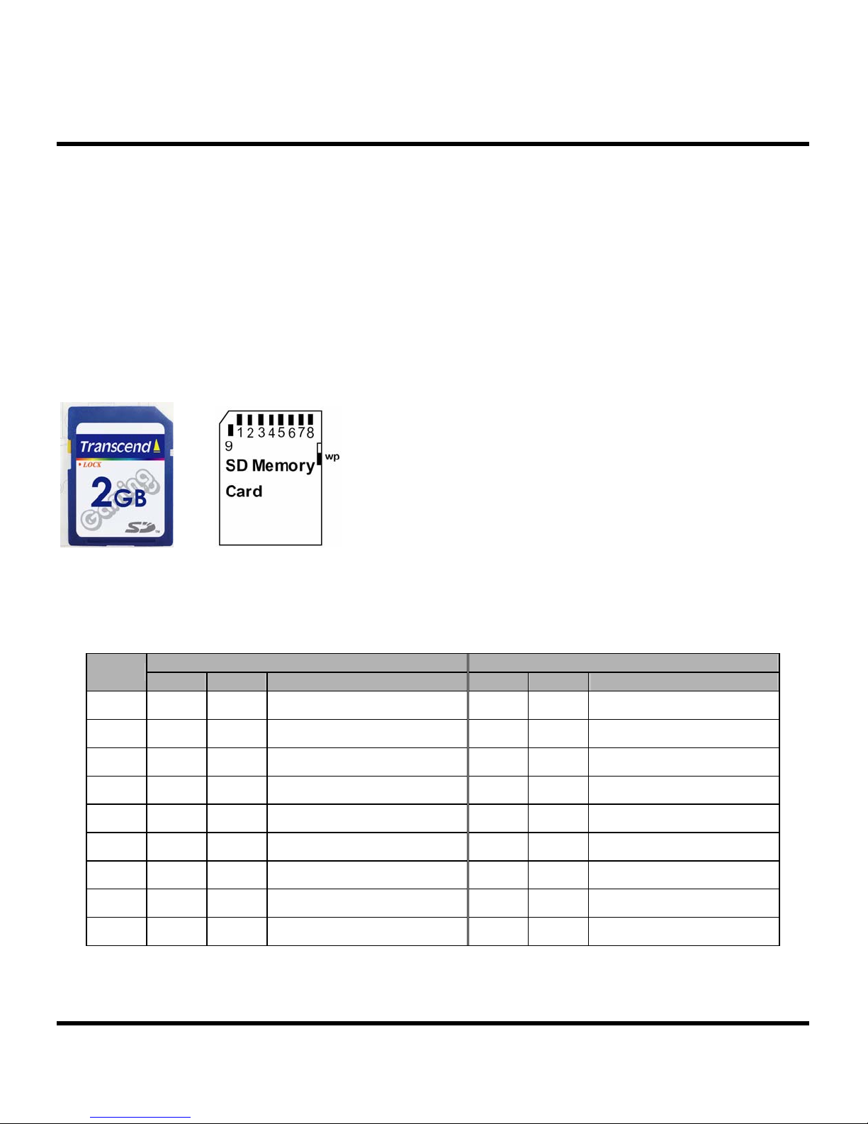
Secure Digital Card
Features
Secure Digital Card of high capacity but economic
cost. It is specifically designed to meet the security,
capacity and small form factor requirements in newly
emerging audio and video consumer electronic
devices. Transcend Secure Digital Card can lead you
to a colorful digital world.
Placement
Front Back
• ROHS compliant product
• Operating Voltage: 2.7 ~ 3.6V
• Operating Temperature: -25 ~ 85°C
• Insertion/removal durability: 10,000 cycles
• Fully compatible with SD card spec. v1.1
• Mechanical Write Protection Switch
• Forward compatibility to MultiMediaCard Version 2.11
• Supports Copy Protection for Recorded Media(CPRM) for
music and other commercial media
• Form Factor: 24mm x 32mm x 2.1mm
Pin Definition
Pin No.
1
2
3
4
5
6
7
8
9
Transcend Information Inc.
Name Type Description Name Type Description
CD/DAT
CMD PP Command/Response
V
SS1
V
DD
CLK I Clock
V
SS2
DAT0 I/O/PP Data Line [Bit0]
DAT1 I/O/PP Data Line [Bit1]
DAT2
3
I/O/PP
S Supply voltage ground
S Supply voltage
S Supply voltage ground
I/O/PP Data Line [Bit2] RSV
SD Mode SPI Mode
Card Detect/Data Line [Bit3]
1
CS I
DI I
VSS S
VDD S
SCLK I
VSS2 S
DO O/PP
RSV
Chip Select (neg true)
Data In
Supply voltage ground
Supply voltage
Clock
Supply voltage ground
Data Out
Page 2
T
S
1
G
~
2
G
S
T
S
1
G
~
2
T
S
1
G
~
2
G
G
S
S
D
D
D
G
G
G
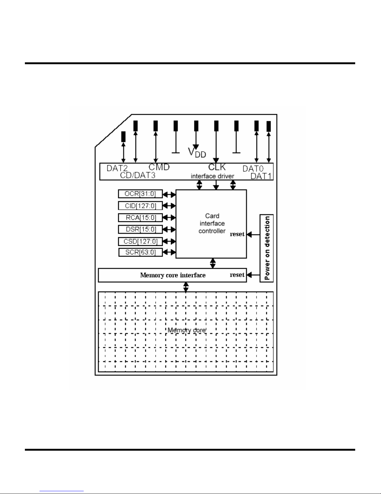
Secure Digital Card
Architecture
Transcend Information Inc.
2
Page 3
SS1
G
G
G
DD
, V
) -0.3 0.3 V
SS2
2.0 3.6 V CMD0, 15,55,ACMD41
Secure Digital Card
commands
ACMD41 commands
DD
T
S
1
G
~
2
G
S
T
S
1
G
~
2
T
S
1
G
Bus Operating Conditions
• General
Peak voltage on all lines -0.3 VDD+0.3 V
All Inputs
Input Leakage Current -10 10 µA
All Outputs
Output Leakage Current -10 10 µA
• Power Supply Voltage
Supply voltage V
Supply voltage specified in OCR register 2.7 3.6 V Except CMD0, 15,55,
Supply voltage differentials (V
Power up time 250 ms From 0v to V
Note. The current consumption of any card during the power-up procedure must not exceed 10 mA.
G
~
2
G
Parameter Symbol Min. Max. Unit Remark
Parameter Symbol Min. Max. Unit Remark
S
S
D
D
D
• Bus Signal Line Load
Min.
The total capacitance C
capacitance C
C
= C
L
HOST
Where N is the number of connected cards. Requiring the sum of the host and bus capacitances not to exceed 30 pF for
up to 10 cards, and 40 pF for up to 30 cards, the following values must not be exceeded:
Bus signal line capacitance C
Single card capacitance C
Maximum signal line inductance 16 nH f
Pull-up resistance inside card (pin1) R
Note that the total capacitance of CMD and DAT lines will be consist of C
connected separately to the SD Memory Card host.
Pull-up resistance R
Bus signal line capacitance C
Transcend Information Inc.
itself and the capacitance C
BUS
+ C
BUS
Parameter Symbol Min. Max. Unit Remark
Parameter Symbol Min. Max. Unit Remark
the CLK line of the SD Memory Card bus is the sum of the bus master capacitance C
L
of each card connected to this line:
CARD
+ Ν*C
CARD
CMD
L
CARD
DAT3
, R
L
DAT
100 pF f
10 pF
10 90 kΩ May be used for card
, C
HOST
10 100 kΩ To prevent bus floating
250 pF f
3
and one C
BUS
≤ 20 MHz, 7 cards
PP
≤ 20 MHz
PP
detection
≤ 5 MHz, 21 cards
PP
HOST
only since they are
CARD
, the bus
Page 4

T
S
1
G
~
2
G
S
T
S
1
G
~
2
T
S
1
G
• Bus Signal Levels
As the bus can be supplied with a variable supply voltage, all signal levels are related to the supply voltage.
~
2
G
G
S
S
D
D
D
G
G
G
Secure Digital Card
To meet the requirements of the JEDEC specification JESD8-1A, the card input and output voltages shall be within the
following specified ranges for any V
Parameter Symbol Min. Max. Unit Remark
Output HIGH voltage V
Output LOW voltage V
Input HIGH voltage V
Input LOW voltage V
Transcend Information Inc.
of the allowed voltage range:
DD
OH
OL
IH
IL
0.75* V
0.625* V
V
DD
0.125* V
DD
– 0.3 0.25* V
SS
4
V I
DD
V
+ 0.3 V
DD
DD
= -100 μA @VDD min
OH
V I
V
= -100 μA @VDD min
OL
Page 5

T
S
1
T
S
1
T
S
1
• Bus Timing
G
G
G
~
~
~
2
2
2
G
G
G
S
S
S
D
D
D
G
G
G
Secure Digital Card
Parameter Symbol Min Max. Unit Remark
Clock CLK (All values are referred to min (VIH) and max (VIL)
Clock frequency Data Transfer Mode f
Clock frequency Identification Mode
(The low freq. is required for MultiMediaCard
compatibility.)
Transcend Information Inc.
PP
f
OD
t
WL
t
WH
t
TLH
50 ns C
0 25 MHz C
0 400 KHz C
10 ns C
50 ns C
10 ns C
50 ns C
10 ns C
5
≤ 100 pF, (7 cards)
L
≤ 250 pF, (21 cards)
L
≤ 100 pF, (7 cards) Clock low time
L
≤ 250 pF, (21 cards)
L
≤ 100 pF, (7 cards) Clock high time
L
≤ 250 pF, (21 cards)
L
≤ 100 pF, (7 cards) Clock rise time
L
≤ 250 pF, (21 cards)
L
Page 6

T
S
1
G
~
2
G
S
T
S
1
G
~
2
T
S
1
G
Inputs CMD, DAT (referenced to CLK)
Input set-up time t
Input hold time t
Outputs CMD, DAT (referenced to CLK)
Output Delay time t
~
2
G
G
S
S
D
D
D
G
G
G
t
THL
50 ns C
ISU
IH
ODLY
10 ns C
5 ns C
5 ns C
0 14 ns C
Secure Digital Card
≤ 100 pF, (7 cards) Clock fall time
L
≤ 250 pF, (21 cards)
L
≤ 25 pF, (1 cards)
L
≤ 25 pF, (1 cards)
L
≤ 25 pF, (1 cards)
L
Transcend Information Inc.
6
Page 7

T
S
1G
T
S
T
S
Reliability and Durability
Temperature Operation: -25°C / 85°C
Moisture and corrosion Operation: 25°C / 95% rel. humidity
Durability 10.000 mating cycles; test procedure: tbd.
Bending 10N
Torque 0.15N.m or +/-2.5 deg
Drop test 1.5m free fall
UV light exposure UV: 254nm, 15Ws/cm² according to ISO 7816-1
Visual inspection
Shape and form
Minimum moving force of WP witch 40gf (Ensures that the WP switch will not slide while it is inserted to the connector.)
WP Switch cycles minimum 1000 Cycles(@Slide force 0.4N to 5N)
Above technical information is based on industry standard data and tested to be reliable. However, Transcend makes no
warranty, either expressed or implied, as to its accuracy and assumes no liability in connection with the use of this product.
Transcend reserves the right to make changes in specifications at any time without prior notice.
5
~
~
~
2
2
2
G
G
G
S
S
S
DG
D
Secure Digital Card
Storage: -40°C (168h) / 85°C (500h)
Junction temperature: max. 95°C
Storage: 40°C / 93% rel. hum./500h
Salt Water Spray: 3% NaCl/35C; 24h acc. MIL STD Method 1009
No warp page; no mold skin; complete form; no cavities surface smoothness <=
-0.1 mm/cm² within contour; no cracks; no pollution (fat, oil dust, etc.)
Transcend Information Inc.
7
 Loading...