

Page 1
S
D
X
S
D
S
D
Description
X
X
C
C
C
C
C
C
a
a
a
r
d
s
e
r
i
e
s
r
d
s
e
r
d
r
s
e
r
i
e
s
i
e
s
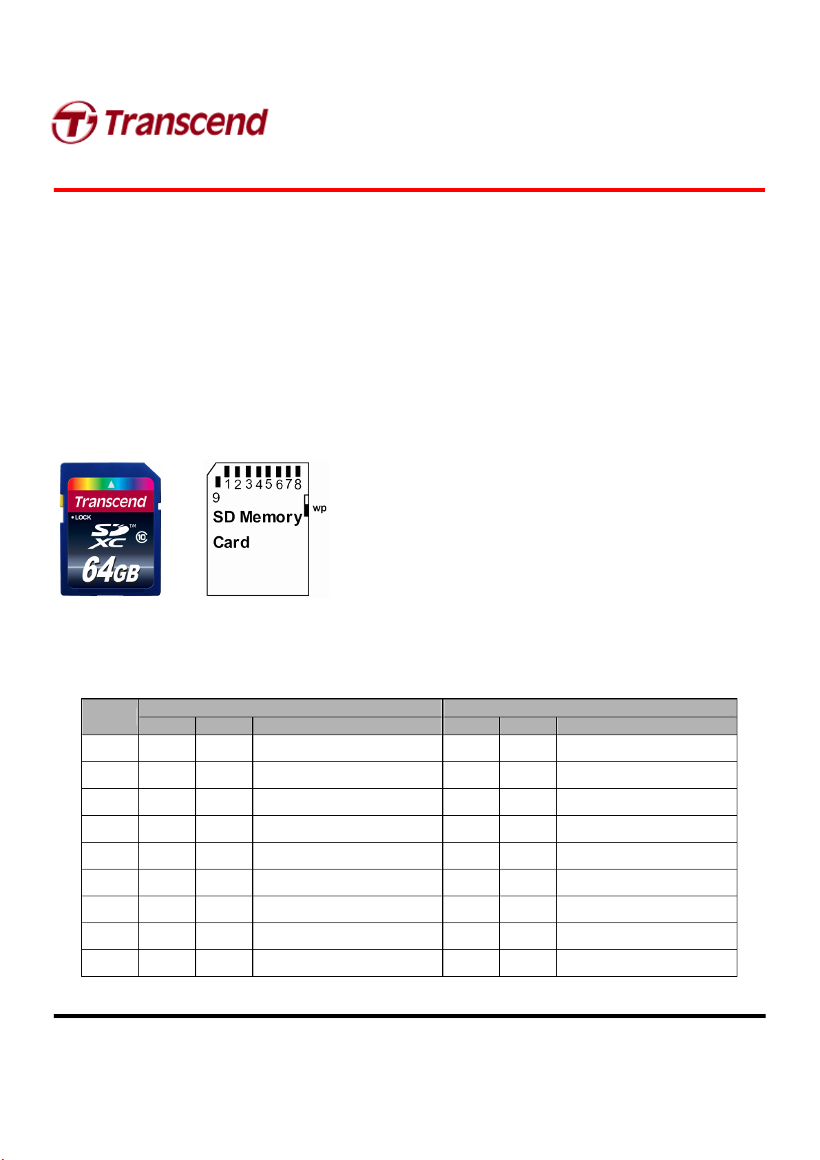
64GB Extended Capacity Secure Digital Card
Features
Rev. 1.0
Transcend secured digital extended capacity Card
series are specifically designed to meet the High
Capacity, High Definition Audio and Full HD Video
requirement for the latest Digital Cameras, DV
Recorders, Mobile, etc,. The new defined Speed
Class enables the host to support AV applications to
perform real time recording to the SD memory card.
Placement
Front Back
•
ROHS compliant product.
•
Card Lid material: PC + ABS
•
Operating Voltage: 2.7 ~ 3.6V
•
Operating Temperature: -25 ~ 85°C
•
Durability: 10,000 insertion/removal cycles
•
Compatible with SD Specification Ver. 3.0
•
Mechanical Write Protection Switch
•
Supports Speed Class 10 Specification
•
Supports Copy Protection for Recorded Media (CPRM)
for SD-Audio
•
Support exFAT file system
•
Form Factor: 24mm x 32mm x 2.1mm
Pin Definition
Pin No.
1
2
3
4
5
6
7
8
9
Transcend Information Inc.
Name Type
CD/DAT
CMD PP Command/Response
V
SS1
V
DD
CLK I Clock
V
SS2
DAT0 I/O/PP Data Line [Bit0]
DAT1 I/O/PP Data Line [Bit1]
DAT2
SD Mode SPI Mode
Description Name Type
I/O/PP
I/O/PP Data Line [Bit2] RSV
Card Detect/Data Line [Bit3]
S Supply voltage ground
S Supply voltage
S Supply voltage ground
CS I
DI I
VSS S
VDD S
SCLK
VSS2
DO O/PP
RSV
1
I
S
Description
Chip Select (neg true)
Data In
Supply voltage ground
Supply voltage
Clock
Supply voltage ground
Data Out
Page 2
S
D
X
C
C
a
S
D
X
D
X
C
C
S
1.0 Architecture
C
C
a
a
r
r
r
d
d
d
s
e
r
i
e
s
s
e
r
s
e
r
i
e
s
i
e
s
64GB Extended Capacity Secure Digital Card
Rev. 1.0
Transcend Information Inc.
2
Page 3
S
D
X
C
C
a
r
d
s
e
r
S
D
X
C
C
a
r
d
S
D
X
C
C
a
r
d
2.0 Hardware Interface
2.1
2.1 General
General
2.1 2.1
GeneralGeneral
s
s
e
e
i
r
i
r
i
e
e
e
s
s
s
Rev. 1.0
64GB Extended Capacity Secure Digital Card
Parameter Symbol
Peak voltage on all lines
All Inputs
Input Leakage Current
All Outputs
Output Leakage Current
2.0
2.0 Power Supply Voltage
Power Supply Voltage
2.0 2.0
Power Supply VoltagePower Supply Voltage
Parameter Symbol
Supply voltage V
Output High Voltage VOH 0.75* V
Output Low Voltage VOL 0.125* V
Input High Voltage VIH 0.625* V
Input Low Voltage VIL VSS-0.3 0.25* V
Power up time 250 ms From 0v to V
DD
Min. Max. Unit Remark
-0.3 VDD+0.3
-10 10 µA
-10 10 µA
Min. Max. Unit Remark
2.7 3.6 V
DD
DD
V IOH=-100uA@V
DD
VDD+0.3
DD
V
V IOL=100uA@V
V
V
DD
DD
DD
Min.
Min.
Min.
Transcend Information Inc.
3
Page 4
S
D
X
C
C
a
S
D
X
S
3.0
3.0 Power Scheme
3.0 3.0
3.1
3.1 Power Up
3.1 3.1
C
D
X
C
Power Scheme
Power SchemePower Scheme
Power Up
Power UpPower Up
C
C
a
a
r
r
r
d
d
d
s
e
r
i
e
s
s
e
r
s
e
r
i
e
s
i
e
s
64GB Extended Capacity Secure Digital Card
Rev. 1.0
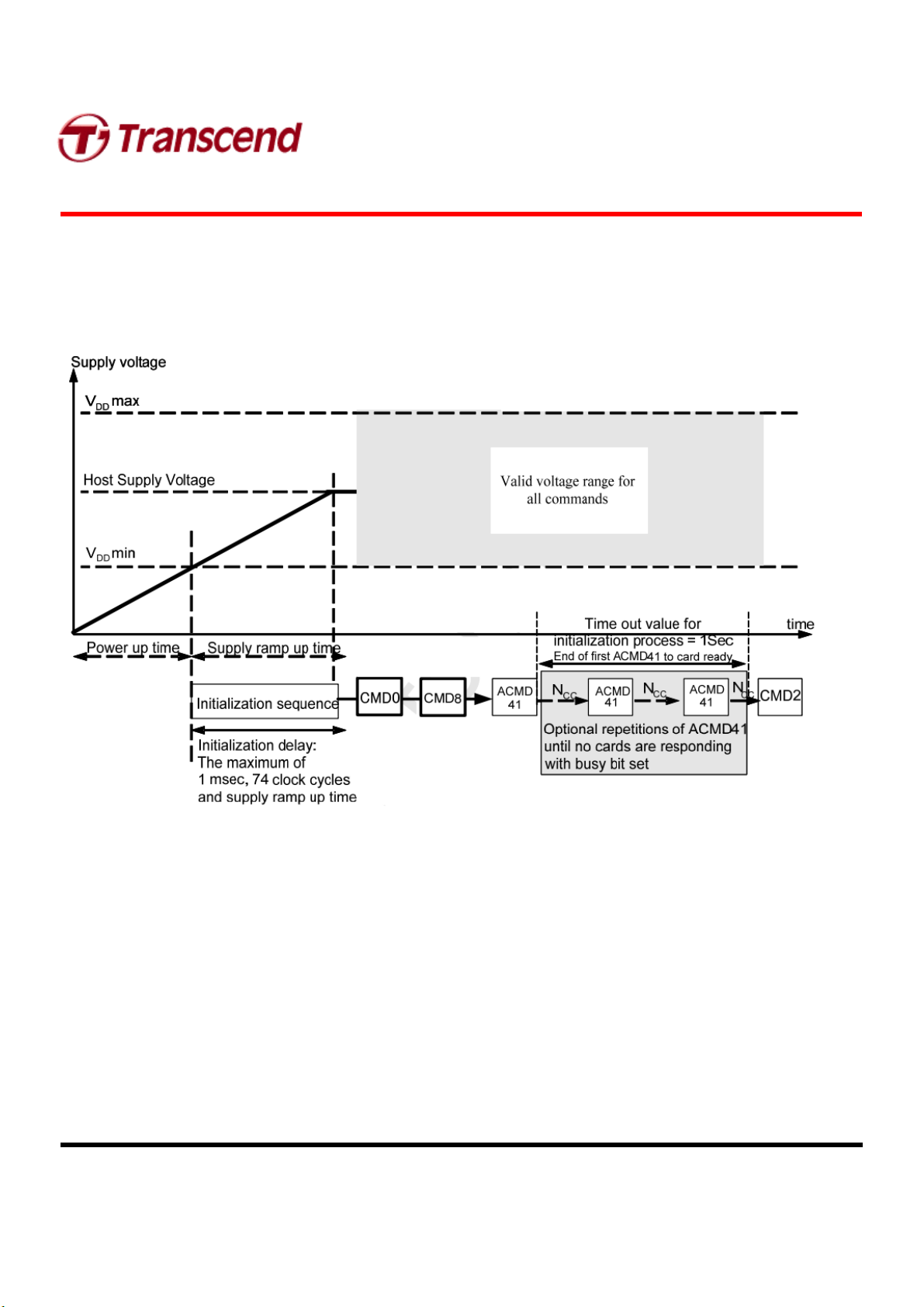
Power up time is defined as voltage rising time from 0 volt to VDD(min.) and depends on application parameters
such as the maximum number of SD Cards, the bus length and the characteristic of the power supply unit.
Supply ramp up time provides the time that the power is built up to the operating level (the host supply voltage)
and the time to wait until the SD card can accept the first command,
The host shall supply power to the card so that the voltage is reached to VDD(min.) within 250ms and start to
supply at least 74 SD clocks to the SD card with keeping CMD line to high. In case of SPI mode, CS shall be
held to high during 74 clock cycles.
Transcend Information Inc.
Power-up Diagram
4
Page 5
S
D
X
C
C
a
r
d
s
e
r
i
e
s
S
D
X
C
C
a
r
d
s
e
S
D
X
C
C
a
r
d
After power up (including hot insertion, i.e. inserting a card when the bus is operating) the SD Card enters the
idle state. In case of SD host, CMD0 is not necessary. In case of SPI host, CMD0 shall be the first command to
send the card to SPI mode.
CMD8 is added in the Physical Layer Specification Version 2.00 to support multiple voltage ranges and used to
check whether the card supports supplied voltage. The version 3.00 host shall issue CMD8 and verify voltage
before card initialization. The host that does not support CMD8 shall supply high voltage range.
ACMD41 is a synchronization command used to negotiate the operation voltage range and to poll the cards
until they are out of their power-up sequence. In case the host system connects multiple cards, the host shall
check that all cards satisfy the supplied voltage. Otherwise, the host should select one of the cards and
initialize
r
s
e
r
i
e
s
i
e
s
64GB Extended Capacity Secure Digital Card
Rev. 1.0
3.2
3.2 Power Up time
3.23.2
Power Up time
Power Up timePower Up time
Host needs to keep power line level less than 0.5V and more than 1ms before power ramp up.
Transcend Information Inc.
5
Page 6

S
D
X
S
S
3.3 Po
C
D
X
C
D
X
C
Powwwwer
PoPo
Followings are requirements for Power on and Power cycle to assure a reliable SD Card hard reset.
(1) Voltage level shall be below 0.5V
(2) Duration shall be at least 1ms.
C
C
C
er On
erer
a
r
d
a
r
d
a
r
d
On or
OnOn
s
e
s
e
s
e
or Po
Powwwwer
oror
PoPo
r
i
e
s
r
i
e
s
r
i
e
s
er CCCCyyyycle
erer
cle
clecle
Rev. 1.0
64GB Extended Capacity Secure Digital Card
3.4 Po
3.5 Po
Powwwwer
PoPo
The power ramp up time is defined from 0.5 V threshold level up to the operating supply voltage which is
stable between VDD(min.) and VDD(max.) and host can supply SDCLK.
Followings are recommendation of Power ramp up:
Powwwwer Do
PoPo
When the host shuts down the power, the card V
of 1ms. During power down, DAT, CMD, and CLK should be disconnected or driven to logical 0 by the host to
avoid a situation that the operating current is drawn through the signal lines.
If the host needs to change the operating voltage, a power cycle is required. Power cycle means the power is
turned off and supplied again. Power cycle is also needed for accessing cards that are already in
To create a power cycle the host shall follow the power down description before power up the card (i.e. the card
V
DD
er Su
Suppppppppllllyyyy Ramp
erer
SuSu
(1) Voltage of power ramp up should be monotonic as much as possible.
(2) The minimum ramp up time should be 0.1ms.
(3) The maximum ramp up time should be 35ms for 2.7-3.6V power supply.
er Dowwwwn and Po
er Doer Do
shall be once lowered to less than 0.5 Volt for a minimum period of 1ms).
Ramp Up
RampRamp
n and Powwwwer C
n and Pon and Po
Up
UpUp
er Cyyyycle
er Cer C
cle
clecle
shall be lowered to less than 0.5 Volt for a minimum period
DD
Inactive State.
3.6
3.6
Current Consumption
3.6 3.6
Transcend Information Inc.
Current Consumption
Current ConsumptionCurrent Consumption
The current consumption is measured by averaging over 1 second.
•
Before first command: Maximum 15 mA
•
During initialization: Maximum 100 mA
•
Operation in Default Mode: Maximum 100 mA
•
Operation in High Speed Mode: Maximum 200 mA
•
Operation with other functions: Maximum 500 mA.
6
Page 7
S
D
X
C
C
a
r
d
s
e
r
i
e
s
S
D
X
C
C
a
r
d
s
e
S
D
X
C
C
a
r
d
4.0
4.0 Bus Signal
Bus Signal
4.0 4.0
Bus SignalBus Signal
4.1
4.1 Bus Signal Levels
Bus Signal Levels
4.1 4.1
Bus Signal LevelsBus Signal Levels
As the bus can be supplied with a variable supply voltage, all signal levels are related to the supply voltage.
r
s
e
r
i
e
s
i
e
s
64GB Extended Capacity Secure Digital Card
Rev. 1.0
To meet the requirements of the JEDEC specification JESD8-1A and JESD8-7, the card input and output voltages shall
be within the following specified ranges for any V
Parameter Symbol Min. Max. Unit Remark
Output HIGH voltage V
Output LOW voltage V
Input HIGH voltage V
Input LOW voltage V
Transcend Information Inc.
OH
OL
IH
IL
of the allowed voltage range:
DD
0.75* VDD V I
0.125* VDD V I
0.625* VDD V
VSS – 0.3 0.25* VDD V
7
+ 0.3 V
DD
= -100 µA @VDD min
OH
= -100 µA @VDD min
OL
Page 8
S
D
X
D
D
X
X
C
C
C
S
S
4.2
4.2 Bus Timing
Bus Timing (Default speed mode)
4.2 4.2
Bus TimingBus Timing
C
a
r
d
s
e
r
i
e
C
a
r
d
s
C
a
r
(Default speed mode)
(Default speed mode) (Default speed mode)
d
e
s
e
s
r
i
e
s
r
i
e
s
Rev. 1.0
64GB Extended Capacity Secure Digital Card
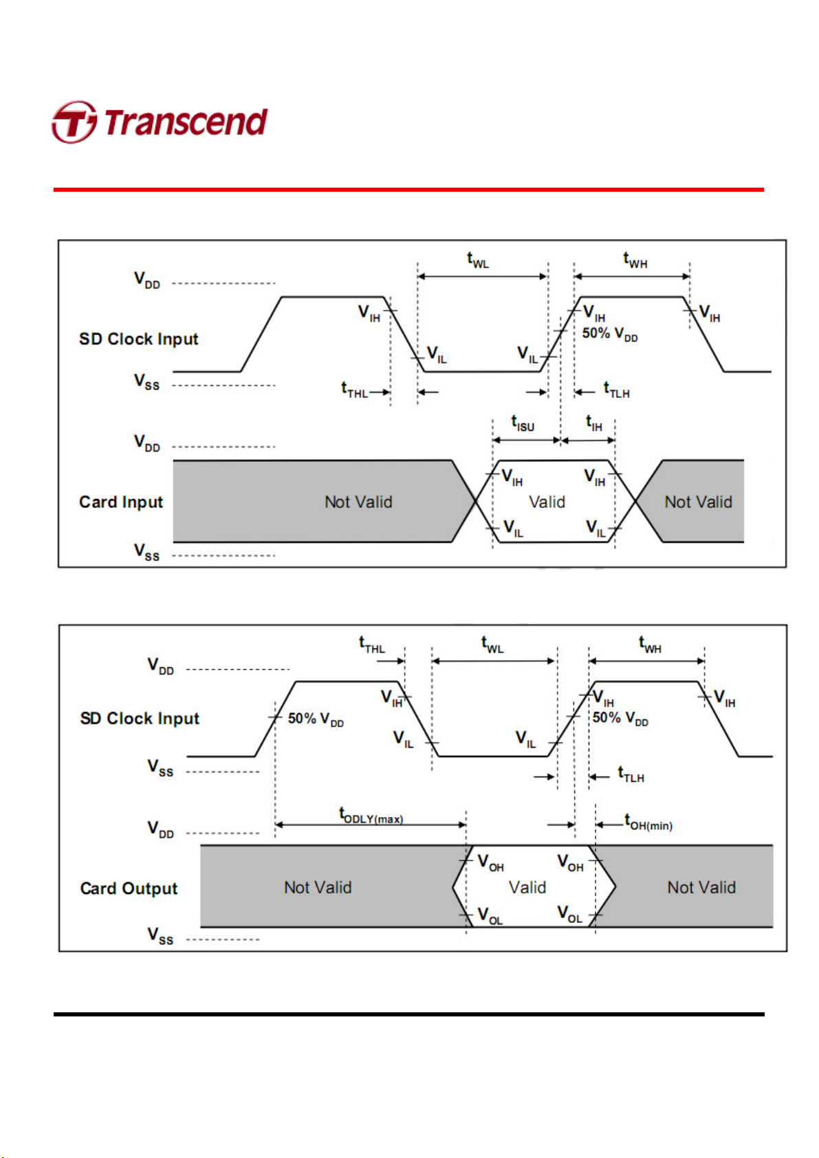
Card Input Timing (Default Speed Mode)
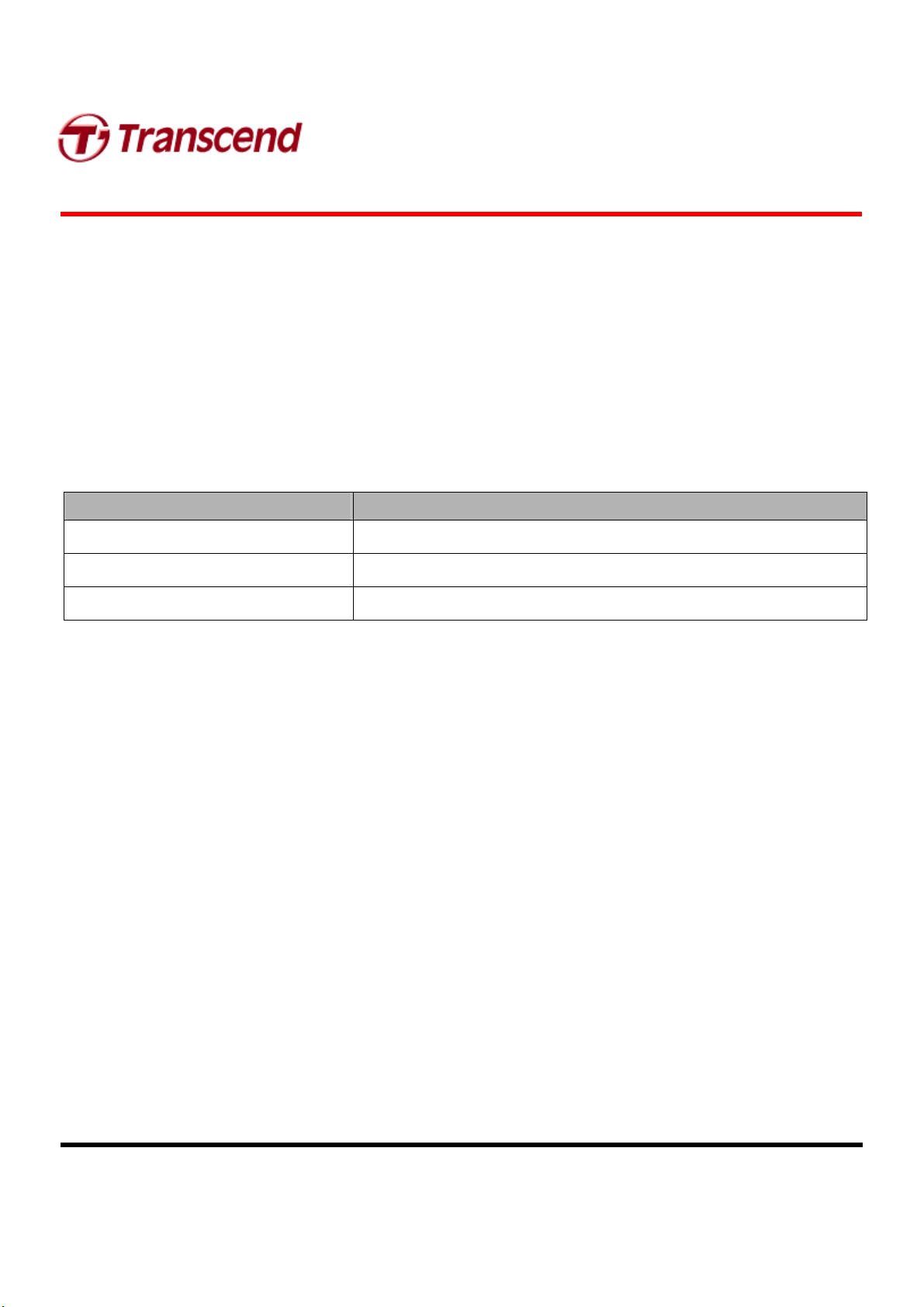
Card Output Timing (Default Speed Mode)
Transcend Information Inc.
8
Page 9
S
D
X
C
C
a
r
d
s
e
r
i
e
s
S
D
X
C
C
a
r
d
s
e
S
D
X
C
C
a
r
d
Parameter Symbol Min Max. Unit Remark
Clock CLK (All values are referred to min (VIH) and max (VIL)
Clock frequency Data Transfer Mode f
Clock frequency Identification Mode f
Clock low time t
Clock high time t
Clock rise time t
Clock fall time t
Inputs CMD, DAT (referenced to CLK)
Input set-up time t
Input hold time t
Outputs CMD, DAT (referenced to CLK)
Output Delay time during Data Transfer Mode t
Output Delay time during Identification Mode t
* 0 Hz means to stop the clock. The given minimum frequency range is for cases were continues clock is required
r
s
e
r
i
e
s
i
e
s
64GB Extended Capacity Secure Digital Card
PP
OD
WL
WH
10 ns
TLH
10 ns
THL
ISU
IH
ODLY
0 50 ns
ODLY
0 25 MHz
0
/100 400 KHz
(1)
10 ns
10 ns
5 ns C
5 ns
0 14 ns
Rev. 1.0
≤
C
C
C
C
C
C
C
C
C
10 pF, (1 card)
CARD
≤
10 pF, (1 card)
CARD
≤
10 pF, (1 card)
CARD
≤ 10 pF, (1 card)
CARD
≤
10 pF, (1 card)
CARD
≤ 10 pF, (1 card)
CARD
≤
10 pF, (1 card)
CARD
≤
10 pF, (1 card)
CARD
≤
40 pF, (1 card)
L
≤
40 pF, (1 card)
L
Transcend Information Inc.
9
Page 10
S
D
X
C
C
a
r
d
s
e
r
i
e
s
S
D
X
C
C
a
r
d
s
e
S
D
X
C
C
a
r
d
4.3
4.3 Bus Timing (High Speed Mode)
Bus Timing (High Speed Mode)
4.3 4.3
Bus Timing (High Speed Mode)Bus Timing (High Speed Mode)
r
s
e
r
i
e
s
i
e
s
Rev. 1.0
64GB Extended Capacity Secure Digital Card
Card Input Timing (High Speed Mode)
Card Output Timing (High Speed Mode)
Transcend Information Inc.
10
Page 11

S
D
X
C
C
a
r
d
s
e
r
i
e
s
S
D
X
C
C
a
r
d
s
e
S
D
X
C
C
a
r
d
Parameter Symbol Min Max. Unit Remark
Clock CLK (All values are referred to min (VIH) and max (VIL)
Clock frequency Data Transfer Mode f
Clock low time t
Clock high time t
Clock rise time t
Clock fall time t
Inputs CMD, DAT (referenced to CLK)
Input set-up time t
Input hold time t
Outputs CMD, DAT (referenced to CLK)
Output Delay time during Data Transfer Mode t
Output Hold time t
Total System capacitance for each line1 CL 40 pF (1 card)
* In order to satisfy severe timing, host shall drive only one card.
* TS64GSDXC10 does not support UHS-I mode.
r
s
e
r
i
e
s
i
e
s
64GB Extended Capacity Secure Digital Card
PP
WL
WH
3 ns
TLH
3 ns
THL
ISU
IH
ODLY
OH
0 50 MHz
7 ns
7 ns
6 ns
2 ns
14 ns
2.5 ns
Rev. 1.0
C
C
C
C
C
C
C
C
C
≤
10 pF, (1 card)
CARD
≤
10 pF, (1 card)
CARD
≤
10 pF, (1 card)
CARD
≤
10 pF, (1 card)
CARD
≤
10 pF, (1 card)
CARD
≤ 10 pF, (1 card)
CARD
≤
10 pF, (1 card)
CARD
≤
40 pF, (1 card)
L
≤
40 pF, (1 card)
L
4.4
4.4 Bus Signal Line Load
Bus Signal Line Load
4.4 4.4
Bus Signal Line LoadBus Signal Line Load
The total capacitance C
capacitance C
Where N is the number of connected cards.
Pull-up resistance R
Bus signal line capacitance CL 40 pF 1 card
Single card capacitance C
Maximum signal line inductance 16 nH f
Pull-up resistance inside card (pin1) R
Note that the total capacitance of CMD and DAT lines will be consist of C
BUS
C
= C
L
HOST
Parameter Symbol
the CLK line of the SD Memory Card bus is the sum of the bus master capacitance C
L
itself and the capacitance C
+ C
BUS
+ Ν
*C
CARD
of each card connected to this line:
CARD
Min. Max. Unit Remark
CMD
R
DAT
10 pF
CARD
DAT3
10 100 kΩ To prevent bus floating
10 90 kΩ May be used for card
HOST
, C
BUS
and one C
C
HOST+CBUS
30 pF
≤
20 MHz
PP
detection
only because they are
CARD
, the bus
HOST
shall not exceed
Transcend Information Inc.
11
Page 12
S
D
X
C
C
a
r
d
s
e
r
i
e
s
S
D
X
C
C
a
r
d
s
e
S
D
X
C
C
a
r
d
connected separately to the SD Memory Card host.
r
s
e
r
i
e
s
i
e
s
Rev. 1.0
64GB Extended Capacity Secure Digital Card
Host should consider total bus capacitance for each signal as the sum of C
defined by per signal. The host can determine C
capacitance load (CL=40 pF). The SD Memory Card guarantees its bus timing when total bus capacitance is less than
maximum value of CL (40 pF).
4.5
4.5 Timeout Condition
4.54.5
Timeout Condition
Timeout ConditionTimeout Condition
Access time Timeout Condition
Read Access time 100ms (Maximum for Single/Multiple Read)
Write Access time 500ms (Maximum for Single/Multiple Write)
Erase Access time 250ms (Maximum for Erase)
HOST
and C
so that total bus capacitance is less than the card estimated
BUS
HOST
, C
BUS
, and C
, these parameters are
CARD
Transcend Information Inc.
12
Page 13

S
D
X
C
C
a
r
d
s
e
r
i
e
s
S
D
X
C
C
a
r
d
s
e
S
D
X
C
C
a
r
d
5.0 Register Information
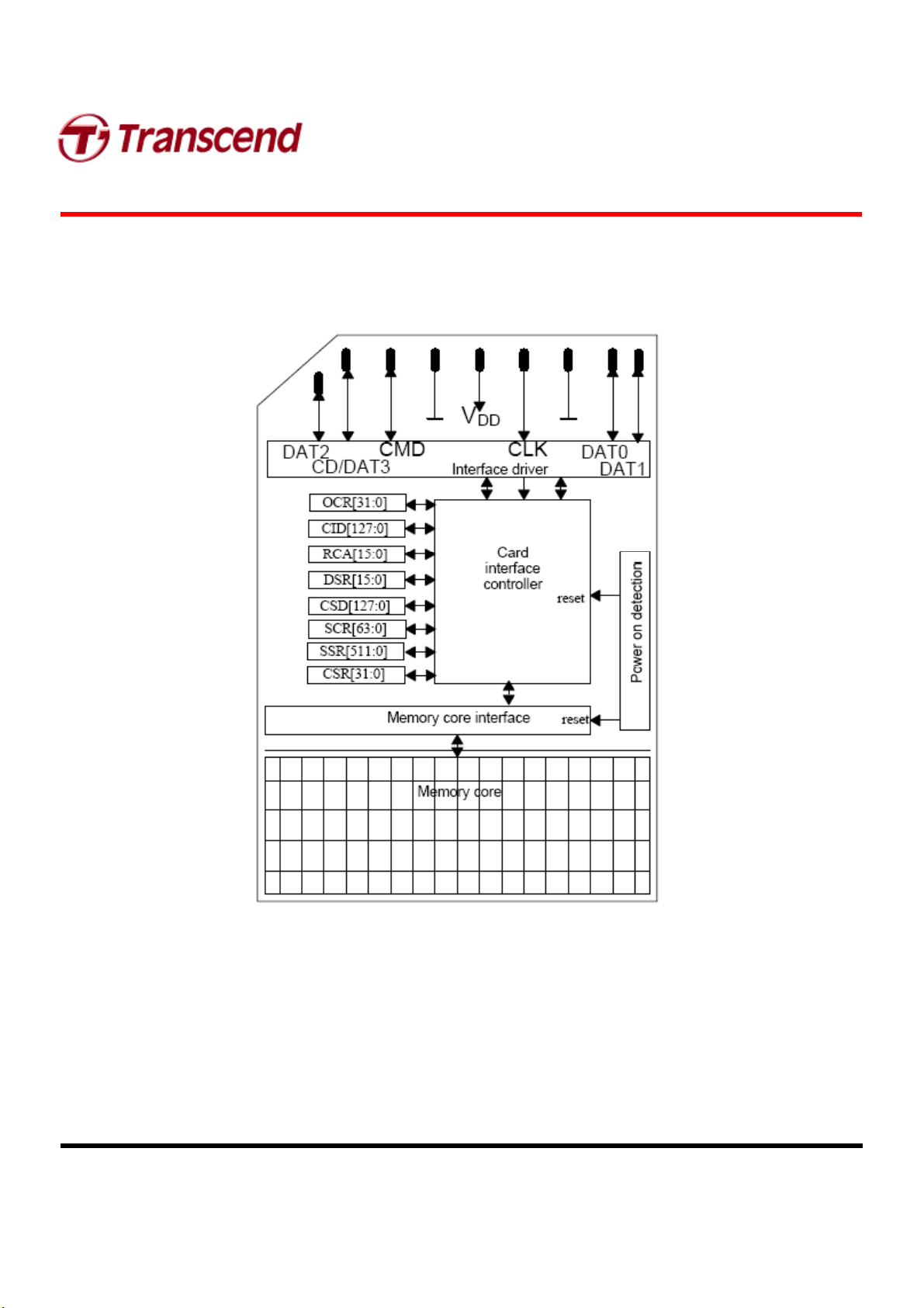
Within the card interface six registers are defined: OCR, CID, CSD, RCA, DSR and SCR. These can be accessed only
by corresponding commands. The OCR, CID, CSD and SCR registers carry the card/content specific information,
while the RCA and DSR registers are configuration registers storing actual configuration parameters.
5.1
5.1 OCR register
OCR register
5.1 5.1
OCR registerOCR register
The 32-bit operation conditions register stores the VDD voltage profile of the card. Additionally, this register includes
status information bits. One status bit is set if the card power up procedure has been finished. This register includes
another status bit indicating the card capacity status after set power up status bit. The OCR register shall be
implemented by the cards. The 32-bit operation conditions register stores the VDD voltage profile of the card. Bit 7 of
OCR is newly defined for Dual Voltage Card and set to 0 in default. If a Dual Voltage Card does not receive CMD8,
r
s
e
r
i
e
s
i
e
s
64GB Extended Capacity Secure Digital Card
Rev. 1.0
OCR bit 7 in the response indicates 0, and the Dual Voltage Card which received CMD8, sets this bit to 1.
Additionally, this register includes 2 more status information bits.
Bit 31 - Card power up status bit, this status bit is set if the card power up procedure has been finished.
Bit 30 - Card Capacity Status bit, 0 indicates that the card is SDSC.
Card Capacity Status bit is valid after the card power up procedure is completed and the card power up
status
The OCR register shall be implemented by the cards.
1 indicates that the card is SDHC or SDXC
. The
Transcend Information Inc.
13
Page 14

S
D
X
C
C
a
r
d
s
e
r
i
e
s
S
D
X
C
C
a
r
d
s
e
S
D
X
C
C
a
r
d
r
s
e
r
i
e
s
i
e
s
64GB Extended Capacity Secure Digital Card
Rev. 1.0
OCR Register Definition
1) This bit is valid only when the card power up status bit is set.
2) This bit is set to LOW if the card has not finished the power up routine.
3) Only UHS-I card supports this bit.
A voltage range is not supported if the corresponding bit value is set to LOW. As long as the card is busy, the
corresponding bit (31) is set to LOW.
5.2 CID Register
The Card Identification (CID) register is 128 bits wide. It contains the card identification information used during the
card identification phase. Every individual flash card shall have a unique identification number. The structure of the
CID register is defined in the following paragraphs:
Transcend Information Inc.
14
Page 15

Product name
PNM
40
[103:64]
S
D
X
C
C
a
r
d
s
e
r
i
e
s
S
D
X
C
C
a
r
d
s
e
S
D
X
C
C
a
r
d
Name
r
s
e
r
i
e
s
i
e
s
Field
64GB Extended Capacity Secure Digital Card
Width CID-slice
Rev. 1.0
Manufacturer ID
OEM/Application ID
Product revision
Product serial number
reserved
Manufacturing date
CRC7 checksum
not used, always 1
•
MID
An 8-bit binary number that identifies the card manufacturer. The MID number is controlled, defined,and allocated to a
SD Memory Card manufacturer by the SD-3C, LLC. This procedure is established to ensure uniqueness of the CID
MID
OID
PRV
PSN
--
MDT
CRC
-
The CID
8
16
8
32
4
12
7
1
Fields
[127:120]
[119:104]
[63:56]
[55:24]
[23:20]
[19:8]
[7:1]
[0:0]
register.
•
OID
A 2-character ASCII string that identifies the card OEM and/or the card contents (when used as a distribution media
either on ROM or FLASH cards). The OID number is controlled, defined, and allocated to a SD Memory Card
manufacturer by the SD-3C, LLC. This procedure is established to ensure uniqueness of the CID register.
Note: SD-3C, LLC licenses companies that wish to manufacture and/or sell SD Memory Cards, including but not limited to flash memory,
ROM, OTP, RAM, and SDIO Combo Cards.
SD-3C, LLC is a limited liability company established by Matsushita Electric Industrial Co. Ltd., SanDisk Corporation and Toshiba
Corporation.
•
PNM
The product name is a string, 5 ASCII characters long.
Transcend Information Inc.
15
Page 16

S
D
X
C
C
a
r
d
s
e
r
i
e
s
S
D
X
C
C
a
r
d
s
e
S
D
X
C
C
a
r
d
•
PRV
The product revision is composed of two Binary Coded Decimal (BCD) digits, four bits each, representing an “n.m”
revision number. The “n” is the most significant nibble and “m” is the least significant nibble.
As an example, the PRV binary value field for product revision “6.2” will be: 0110 0010b
•
PSN
The Serial Number is 32 bits of binary number.
•
MDT
The manufacturing date composed of two hexadecimal digits, one is 8 bit representing the year(y)
and the other is four bits representing the month(m).
The “m” field [11:8] is the month code. 1 = January.
The “y” field [19:12] is the year code. 0 = 2000.
r
s
e
r
i
e
s
i
e
s
64GB Extended Capacity Secure Digital Card
Rev. 1.0
As an example, the binary value of the Date field for production date “April 2001” will be:
00000001 0100.
•
CRC
CRC7 checksum (7 bits).
5.3 CSD Register
The CSD Regsiter shows Definition of the CSD for the High Capacity SD Memory Card and Extended Capacity SD
Memory Card (CSD Version 2.0). The following sections describe the CSD fields and the relevant data types for the
High Capacity SD Memory Card.
CSD Version 2.0 is applied to SDHC and SDXC Cards. The field name in parenthesis is set to fixed value and
indicates that the host is not necessary to refer these fields. The fixed values enables host,which refers to these fields,
to keep compatibility to CSD Version 1.0. The Cell Type field is coded as follows: R = readable, W(1) = writable once,
W = multiple writable.
Name
CSD structure
Field
CSD_STRUCTURE
Width Value
2
01b
Cell Type CSD-slice
R
[127:126]
reserved
data read access-time
Transcend Information Inc.
-
(TAAC)
6
8
16
00 0000b
0Eh
R
R
[125:120]
[119:112]
Page 17

S
D
X
C
C
a
r
d
s
e
r
i
e
s
S
D
X
C
C
a
r
d
s
e
S
D
X
C
C
a
r
d
r
s
e
r
i
e
s
i
e
s
64GB Extended Capacity Secure Digital Card
Rev. 1.0
data read access-time in CLK (NSAC)
max. data transfer rate
card command classes
max. read data block length (READ_BL_LEN)
partial blocks for read allowed (READ_BL_PARTIAL)
write block misalignment
read block misalignment
DSR implemented
reserved
device size
reserved
erase single block enable
erase sector size
write protect group size
(TRAN_SPEED)
CCC
(WRITE_BLK_MISALIGN) 1
(READ_BLK_MISALIGN) 1
DSR_IMP
-
C_SIZE
-
(ERASE_BLK_EN)
(SECTOR_SIZE)
(WP_GRP_SIZE)
8
8
12
4
1
1
6
22
1
1
7
7
00h
32h, 5Ah, 0Bh or 2Bh
01x110110101b
9
0
0
0
x
00 0000b
xxxxxxh
0
1
7Fh
0000000b
R
R
R
R
R
R
R
R
R
R
R
R
R
R
[111:104]
[103:96]
[95:84]
[83:80]
[79:79]
[78:78]
[77:77]
[76:76]
[75:70]
[69:48]
[47:47]
[46:46]
[45:39]
[38:32]
write protect group enable
reserved
write speed factor
max. write data block length (WRITE_BL_LEN)
partial blocks for write allowed (WRITE_BL_PARTIAL)
reserved
File format group
copy flag
permanent write protection
temporary write protection
File format
Transcend Information Inc.
(WP_GRP_ENABLE)
(R2W_FACTOR)
-
(FILE_FORMAT_GRP)
COPY
PERM_WRITE_PROTECT 1
TMP_WRITE_PROTECT 1
(FILE_FORMAT)
17
1
2
3
4
1
5
1
1
2
0
00b
010b
9
0
00000b
0
x
x
x
00b
R
R
R
R
R
R
R
R/W(1) [14:14]
R/W(1) [13:13]
R/W
R
[31:31]
[30:29]
[28:26]
[25:22]
[21:21]
[20:16]
[15:15]
[12:12]
[11:10]
Page 18

0
CSD
V
ersion
1.0St
andard C
apacity
S
D
X
C
C
a
r
d
s
e
r
i
e
s
S
D
X
C
C
a
r
d
s
e
S
D
X
C
C
a
r
d
r
s
e
r
i
e
s
i
e
s
64GB Extended Capacity Secure Digital Card
Rev. 1.0
reserved
CRC
not used, always'1'
The following sections describe the CSD fields and the relevant data types. If not explicitly defined otherwise, all bit
strings are interpreted as binary coded numbers starting with the left bit first.
•
CSD_STRUCTURE
Field structures of the CSD register are different depend on the Physical Specification Version and Card
Capacity.
The CSD_STRUCTURE field in the CSD register indicates its structure version.
The following table shows the version number of the related CSD structure.
CSD_STRUCTURE
The CSD Register Fields (CSD Version 2.0)
-
CRC
-
CSD structure version
2
7
1
00b
xxxxxxxb
1
Card Capacity
R
R/W
-
[9:8]
[7:1]
[0:0]
CSD Register Structure
•
TAAC
This field is fixed to 0Eh, which indicates 1 ms. The host should not use TAAC, NSAC, and R2W_FACTOR to calculate
timeout and should uses fixed timeout values for read and write operations.
TAAC bit position code
2:0
Transcend Information Inc.
time unit
0=1ns, 1=10ns, 2=100ns, 3=1µs, 4=10µs,
5=100µs, 6=1ms, 7=10ms
18
Page 19
4=1.5,
S
D
X
C
C
a
r
d
s
e
r
i
e
s
S
D
X
C
C
a
r
d
s
e
S
D
X
C
C
a
r
d
6:3
7
•
NSAC
This field is fixed to 00h. NSAC should not be used to calculate time-out values.
•
TRAN_SPEED
The following table defines the maximum data transfer rate per one data line - TRAN_SPEED:
r
s
e
r
i
e
s
i
e
s
time value
0=reserved, 1=1.0, 2=1.2, 3=1.3,
5=2.0,
6=2.5, 7=3.0, 8=3.5, 9=4.0, A=4.5, B=5.0,
C=5.5, D=6.0, E=7.0, F=8.0
reserved
64GB Extended Capacity Secure Digital Card
Rev. 1.0
2:0
6:3
7
Maximum Data Transfer Rate Definition
Note that for current SD Memory Cards that field must be always 0_0110_010b (032h) which is equal to 25MHz - the
mandatory maximum operating frequency of SD Memory Card.
In High-Speed mode, that field must be always 0_1011_010b (05Ah) which is equal to 50MHz. And when the timing
mode returns to the default by CMD6 or CMD0 command, its value will be 032h.
•
CCC
transfer rate unit
0=100kbit/s, 1=1Mbit/s, 2=10Mbit/s,
3=100Mbit/s, 4... 7=reserved
time value
0=reserved, 1=1.0, 2=1.2, 3=1.3, 4=1.5,
5=2.0, 6=2.5, 7=3.0, 8=3.5, 9=4.0, A=4.5,
B=5.0, C=5.5, D=6.0, E=7.0, F=8.0
reserved
The SD Memory Card command set is divided into subsets (command classes). The card command class register
CCC defines which command classes are supported by this card. A value of ‘1’ in a CCC bit means that the
corresponding command class is supported.
19
Transcend Information Inc.
Page 20

S
D
X
C
C
a
r
d
s
e
r
i
e
s
S
D
X
C
C
a
r
d
s
e
S
D
X
C
C
a
r
d
r
s
e
r
i
e
s
i
e
s
64GB Extended Capacity Secure Digital Card
Rev. 1.0
CCC bit
0
1
......
11
•
READ_BL_LEN
This field is fixed to 9h, which indicates READ_BL_LEN=512 Byte.
•
READ_BL_PARTIAL
This field is fixed to 0, which indicates partial block read is inhibited and only unit of block access is allowed.
•
WRITE_BLK_MISALIGN
This field is fixed to 0, which indicates that write access crossing physical block boundaries is always disabled in SDXC
Cards.
•
READ_BLK_MISALIGN
This field is fixed to 0, which indicates that read access crossing physical block boundaries is always disabled in SDXC
Supported Card Command Classes
Supported card command class
class 0
class 1
class 11
Cards.
•
DSR_IMP
Defines if the configurable driver stage is integrated on the card. If set, a driver stage register (DSR) must be
implemented also
DSR_IMP
0
1
•
C_SIZE
This field is expanded to 22 bits and can indicate up to 2 TBytes (It is the same as the maximum memory space
Transcend Information Inc.
DSR type
no DSR implemented
DSR implemented
DSR Implementation Code Table
20
Page 21

S
D
X
C
C
a
r
d
s
e
r
i
e
s
S
D
X
C
C
a
r
d
s
e
S
D
X
C
C
a
r
d
specified by a 32-bit block address.) This parameter is used to calculate the user data area capacity in the SD memory
card (not include the protected area). The user data area capacity is calculated from C_SIZE as follows:
memory capacity = (C_SIZE+1) * 512K byte
The Minimum user area size of SDHC Card is 4,211,712 sectors (2GB + 8.5MB).
The Minimum value of C_SIZE for SDHC in CSD Version 2.0 is 001010h (4112).
The maximum user area size of SDHC Card is (32GB - 80MB)
The maximum value of C_SIZE for SDHC in CSD Version 2.0 is 00FF5Fh (65375).
The Minimum user area size of SDXC Card is 67,108,864 sectors (32GB).
The Minimum value of C_SIZE for SDXC in CSD Version 2.0 is 00FFFFh (65535).
•
ERASE_BLK_EN
This field is fixed to 1, which means the host can erase one or multiple units of 512 bytes.
•
SECTOR_SIZE
This field is fixed to 7Fh, which indicates 64 KBytes. This value is not related to erase operation. SDXC Cards indicate
r
s
e
r
i
e
s
i
e
s
64GB Extended Capacity Secure Digital Card
Rev. 1.0
memory boundary by AU size and this field should not be used.
•
WP_GRP_SIZE
This field is fixed to 00h. SDXC Cards do not support write protected groups.
•
WP_GRP_ENABLE
This field is fixed to 0. SDXC Cards do not support write protected groups.
•
R2W_FACTOR
This field is fixed to 2h, which indicates 4 multiples. Write timeout can be calculated by multiplying the read access time
and R2W_FACTOR. However, the host should not use this factor and should use 250 ms for write timeout
•
WRITE_BL_LEN
This field is fixed to 9h, which indicates WRITE_BL_LEN=512 Byte.
•
WRITE_BL_PARTIAL
This field is fixed to 0, which indicates partial block read is inhibited and only unit of block access is allowed.
•
FILE_FORMAT_GRP
This field is set to 0. Host should not use this field.
•
COPY
Defines whether the contents is original (=0) or has been copied (=1). Setting this bit to 1 indicates that the card
Transcend Information Inc.
21
Page 22

S
D
X
C
C
a
r
d
s
e
r
i
e
s
S
D
X
C
C
a
r
d
s
e
S
D
X
C
C
a
r
d
content is a copy. The COPY bit is a one time programmable bit except ROM card.
•
PERM_WRITE_PROTECT
Permanently protects the whole card content against overwriting or erasing (all write and erase commands for this card
are permanently disabled). The default value is ‘0’, i.e. not permanently write protected.
•
TMP_WRITE_PROTECT
Temporarily protects the whole card content from being overwritten or erased (all write and erase commands for this
card are temporarily disabled). This bit can be set and reset. The default value is ‘0’, i.e. not write protected.
•
FILE_FORMAT
This field is set to 0. Host should not use this field
•
CRC
The CRC field carries the check sum for the CSD contents.
r
s
e
r
i
e
s
i
e
s
64GB Extended Capacity Secure Digital Card
Rev. 1.0
The checksum has to be recalculated by the host for any CSD modification. The default corresponds to the initial CSD
contents.
The following table lists the correspondence between the CSD entries and the command classes. A ‘+’ entry indicates
that the CSD field affects the commands of the related command class.
5.
5.4 RCA Register
4 RCA Register
5.5.
4 RCA Register4 RCA Register
The writable 16-bit relative card address register carries the card address that is published by the card during the card
identification. This address is used for the addressed host-card communication after the card identification procedure.
The default value of the RCA register is 0x0000. The value0x0000 is reserved to set all cards into the Stand-by State
with CMD7.
5. DSR Register (Optional)
It can be optionally used to improve the bus performance for extended operating conditions (depending on parameters
like bus length, transfer rate or number of cards). The CSD register carries the information about the DSR register
usage. The default value of the DSR register is 0x404.
Transcend Information Inc.
22
Page 23
SCR_STR
UCTURE
SCR struct
u
re version
SD Phy
sical
Layer Specification
Version
S
D
X
C
C
a
r
d
s
e
r
i
e
s
S
D
X
C
C
a
r
d
s
e
S
D
X
C
C
a
r
d
6. SCR Register
In addition to the CSD register there is another configuration register that named - SD CARD Configuration Register
(SCR). SCR provides information on SD Memory Card's special features that were configured into the given card. The
r
s
e
r
i
e
s
i
e
s
64GB Extended Capacity Secure Digital Card
Rev. 1.0
size of SCR register is 64 bit. This register shall be set in the factory by the SD Memory Card manufacturer.
The following table describes the SCR register content.
Description
SCR Structure
SD Memory Card - Spec. Version SD_SPEC
data_status_after erases
CPRM Security Support
DAT Bus widths supported
Spec. Version 3.00 or higher
Extended Security Support
Reserved
Field
SCR_STRUCTURE
DATA_STAT_AFTER_ERASE 1
SD_SECURITY
SD_BUS_WIDTHS
SD_SPEC3
EX_ SECURITY
Width Cell
Type
4
4
3
4
1
4
9
R
R
R
R
R
R
R
R
SCR
Slic
[63:60]
[59:56]
[55:55]
[54:52]
[51:48]
[47]
[46:43]
[42:34]
Command Support bits
reserved for manufacturer usage
•
SCR_STRUCTURE
Version number of the related SCR structure in the SD Memory Card Physical Layer Specification.
0
1-15
Transcend Information Inc.
-
SCR version 1.0
reserved
SCR Register Structure Version
CMD_SUPPORT
The SCR Fields
Version 1.01-3.00
23
14
32
R
R
[33:32]
[31:0]
Page 24

S
D
X
C
C
a
r
d
s
e
r
i
e
s
S
D
X
C
C
a
r
d
s
e
S
D
X
C
C
a
r
d
•
SD_SPEC
Describes the SD Memory Card Physical Layer Specification version supported by this card.
SD_SPEC Physical Layer Specification Version Number
0 Version 1.0-1.01
1 Version 1.10
2
3-15 reserved
•
SD_SPEC3
r
s
e
r
i
e
s
i
e
s
Version 2.00 or Version 3.00
(Refer to SD_SPEC3)
Physical Layer Specification Version
64GB Extended Capacity Secure Digital Card
Rev. 1.0
SD_SPEC SD_SPEC3 Physical Layer Specification Version Number
2
2
The card manufacturer determines SD_SPEC value by conditions indicated below. All conditions shall
be satisfied for each version. The other combination of conditions is not allowed.
Essential conditions to indicate Version 3.00 Card (SD_SPEC=2 and SD_SPEC3=1)
(1) The card shall support CMD6
(2) The card shall support CMD8
(3) The card shall support CMD42
(4) User area capacity shall be up to 2GB (SDSC) or 32GB (SDHC) User area capacity shall be more than
or equal to 32GB and up to 2TB (SDXC)
(5) Speed Class shall be supported (SDHC or SDXC)
Application Notes:
0
1
Version 2.00
Version 3.00
When checking SD_SPEC version in SCR, the host shall not forget that higher SD_SPEC version may be
specified in future. It is important to keep compatibility for future version.
Transcend Information Inc.
24
Page 25

S
D
X
C
C
a
r
d
s
e
r
i
e
s
S
D
X
C
C
a
r
d
s
e
S
D
X
C
C
a
r
d
•
DATA_STAT_AFTER_ERASE
Defines the data status after erase, whether it is ‘0’ or ‘1’ (the status is card vendor dependent).
•
SD_SECURITY
r
s
e
r
i
e
s
i
e
s
64GB Extended Capacity Secure Digital Card
Rev. 1.0
This field indicates CPRM Security Specification Version for each capacity card. The definition of
is different in each capacity card.
SD_SECURITY CPRM Security Version
0
1
2
3
4
5 - 7
The basic rule of setting this field:
SDSC Card sets this field to 2 (Version 1.01)
SDHC Card sets this field to 3 (Version 2.00).
SDXC Card sets this field to 4 (Version 3.xx).
Note that it is mandatory for a regular writable SD Memory Card to support Security Protocol. For ROM (Read
Only) and OTP (One Time Programmable) types of the SD Memory Card, the security feature is optional.
•
SD_BUS_WIDTHS
Describes all the DAT bus widths that are supported by this card.
No Security
Not Used
SDSC Card (Security Version 1.01)
SDHC Card (Security Version 2.00)
SDXC Card (Security Version 3.xx)
CPRM Security Version
Reserved
Protected Area
SD_BUS_WIDTHS
Bit 0
Bit 1
Bit 2
Bit 3
SD Memory Card Supported Bus Widths
Transcend Information Inc.
Supported Bus Widths
1 bit (DAT0)
reserved
4 bit (DAT0-3)
reserved
25
Page 26

S
D
X
C
C
a
r
d
s
e
r
i
e
s
S
D
X
C
C
a
r
d
s
e
S
D
X
C
C
a
r
d
Since SD Memory Card shall support at least the two bus modes 1bit or 4bit width then any SD Card shall set at least
bits 0 and 2 (SD_BUS_WIDTH="0101").
r
s
e
r
i
e
s
i
e
s
64GB Extended Capacity Secure Digital Card
Rev. 1.0
Transcend Information Inc.
26
Page 27

0.1
S
D
X
C
C
a
r
d
s
e
r
i
e
s
S
D
X
C
C
a
r
d
s
e
S
D
X
C
C
a
r
d
6.0 Reliability and Durability
Temperature Operation: -25°C / 85°C
Moisture and corrosion Operation: 25°C / 95% rel. humidity
Durability 10.000 mating cycles; test procedure: tbd.
Bending 10N
Torque 0.15N.m or +/-2.5 deg
Drop test 1.5m free fall
Visual inspection
Shape and form
Minimum moving force of WP witch 40gf (Ensures that the WP switch will not slide while it is inserted to the connector.)
WP Switch cycles minimum 1000 Cycles(@Slide force 0.4N to 5N)
r
s
e
r
i
e
s
i
e
s
Storage: -40°C (168h) / 85°C (500h)
Junction temperature: max. 95°C
Storage: 40°C / 93% rel. hum./500h
Salt Water Spray: 3% NaCl/35C; 24h acc. MIL STD Method 1009
No warp page; no mold skin; complete form; no cavities surface smoothness <= -
mm/cm² within contour; no cracks; no pollution (fat, oil dust, etc.)
64GB Extended Capacity Secure Digital Card
Rev. 1.0
Transcend Information Inc.
27
Page 28
S
D
X
C
C
a
r
d
s
e
r
i
e
S
D
X
C
C
a
r
d
s
S
D
X
C
C
a
r
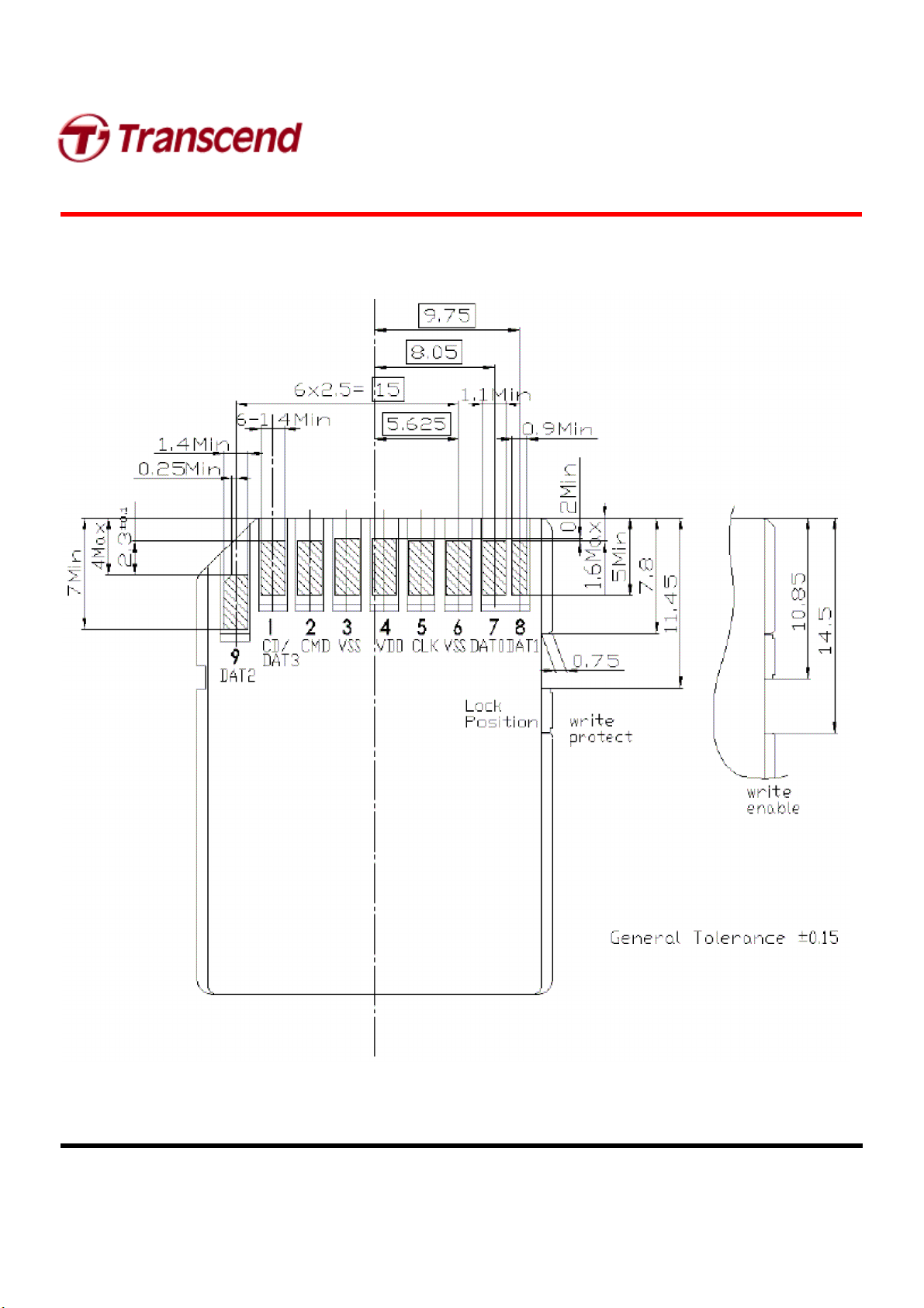
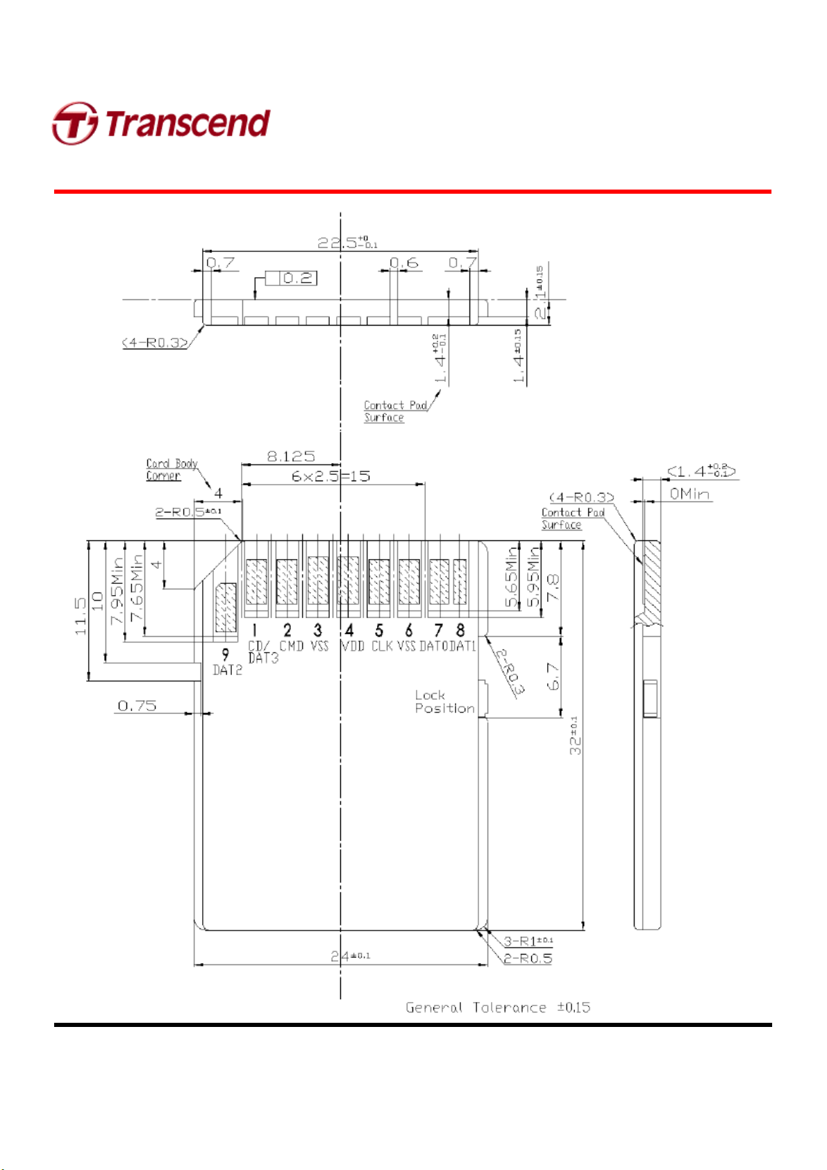
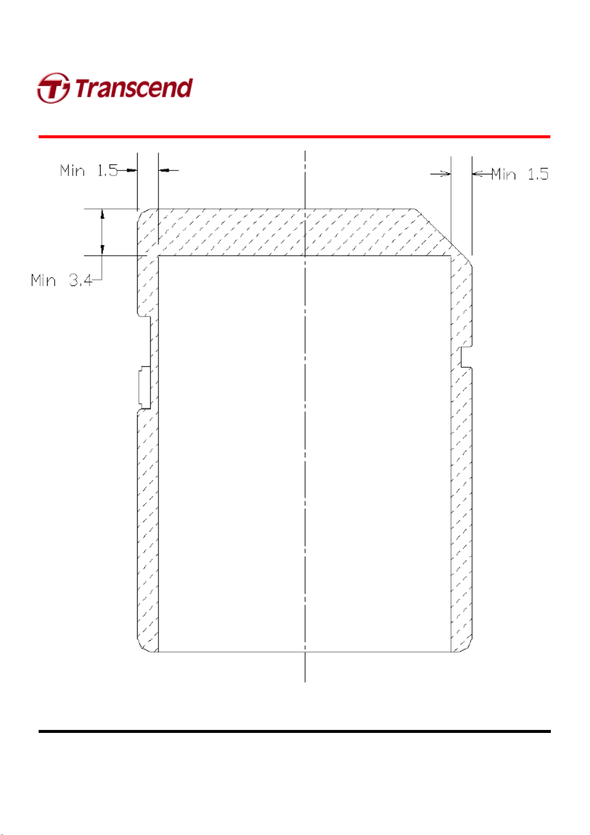
7.0 Mechanical Dimension
d
e
s
e
s
r
i
e
s
r
i
e
s
Rev. 1.0
64GB Extended Capacity Secure Digital Card
Transcend Information Inc.
28
Page 29
S
D
X
C
C
a
r
d
s
e
r
i
e
s
S
D
X
C
C
a
r
d
s
e
S
D
X
C
C
a
r
d
r
s
e
r
i
e
s
i
e
s
64GB Extended Capacity Secure Digital Card
Rev. 1.0
Transcend Information Inc.
29
Page 30
S
D
X
C
C
a
r
d
s
e
r
i
e
s
S
D
X
C
C
a
r
d
s
e
S
D
X
C
C
a
r
d
r
s
e
r
i
e
s
i
e
s
64GB Extended Capacity Secure Digital Card
Rev. 1.0
Transcend Information Inc.
30
 Loading...