

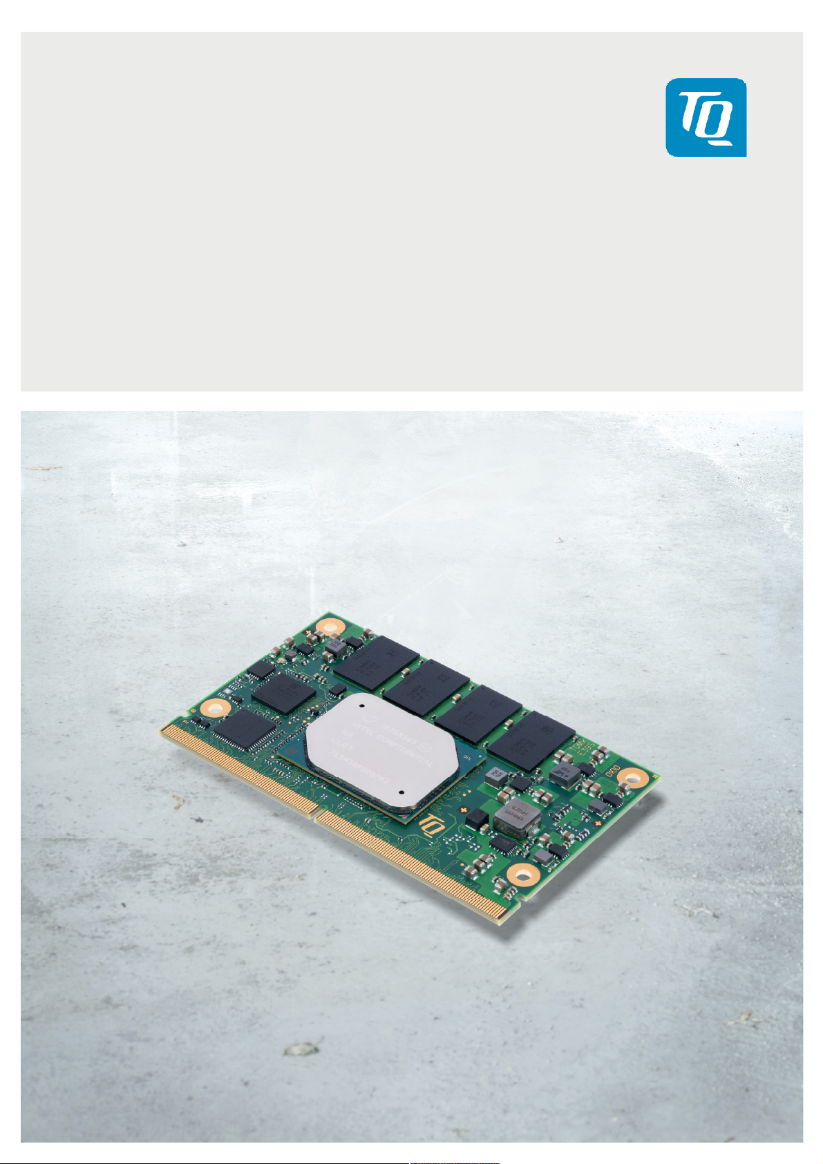
TQMxE39S
User's Manual
TQMxE39S UM 0101
2019-01-15

User's Manual l TQMxE39S UM 0101 l © 2019 TQ-Group Page i
TABLE OF CONTENTS
1. ABOUT THIS MANUAL................................................................................................................................................................................1
1.1 Copyright and Licence Expenses ........................................................................................................................................................... 1
1.2 Registered Trademarks..............................................................................................................................................................................1
1.3 Disclaimer...................................................................................................................................................................................................... 1
1.4 Imprint............................................................................................................................................................................................................1
1.5 Service and Support...................................................................................................................................................................................1
1.6 Tips on Safety ...............................................................................................................................................................................................2
1.7 Symbols and Typographic Conventions..............................................................................................................................................2
1.8 Handling and ESD Tips .............................................................................................................................................................................. 2
1.9 Naming of Signals....................................................................................................................................................................................... 3
1.10 Further Applicable Documents / Presumed Knowledge................................................................................................................ 3
2. INTRODUCTION ........................................................................................................................................................................................... 3
2.1 Functional Overview.................................................................................................................................................................................. 4
2.2 Specification Compliance.........................................................................................................................................................................5
2.3 Variants...........................................................................................................................................................................................................5
2.4 Accessories....................................................................................................................................................................................................5
3. FUNCTION .....................................................................................................................................................................................................6
3.1 Block Diagram..............................................................................................................................................................................................6
3.2 Electrical Characteristics ...........................................................................................................................................................................6
3.2.1 Supply Voltage Characteristics ...............................................................................................................................................................6
3.2.2 Power Consumption ..................................................................................................................................................................................7
3.2.2.1 Real Time Clock............................................................................................................................................................................................8
3.3 Environment.................................................................................................................................................................................................8
3.4 System Components.................................................................................................................................................................................. 9
3.4.1 CPU ..................................................................................................................................................................................................................9
3.4.2 Graphics .........................................................................................................................................................................................................9
3.4.3 Memory....................................................................................................................................................................................................... 10
3.4.3.1 LPDDR4 SDRAM........................................................................................................................................................................................ 10
3.4.3.2 eMMC........................................................................................................................................................................................................... 10
3.4.3.3 SPI Boot Flash ............................................................................................................................................................................................ 10
3.4.3.4 EEPROM....................................................................................................................................................................................................... 10
3.4.4 Real Time Clock......................................................................................................................................................................................... 10
3.4.5 Hardware Monitor.................................................................................................................................................................................... 10
3.4.6 TQ flexible I/O configuration (TQ-flexiCFG) ..................................................................................................................................... 10
3.5 Interfaces .................................................................................................................................................................................................... 11
3.5.1 PCI Express ................................................................................................................................................................................................. 11
3.5.2 Gigabit Ethernet ....................................................................................................................................................................................... 11
3.5.3 Serial ATA.................................................................................................................................................................................................... 11
3.5.4 Digital Display Interface......................................................................................................................................................................... 11
3.5.5 LVDS Interface........................................................................................................................................................................................... 11
3.5.6 USB 2.0 Interfaces..................................................................................................................................................................................... 12
3.5.7 USB 3.0 Interfaces..................................................................................................................................................................................... 12
3.5.8 SD Card Interface...................................................................................................................................................................................... 12
3.5.9 General Purpose Input/Output............................................................................................................................................................ 12
3.5.10 Audio Interface ......................................................................................................................................................................................... 12
3.5.11 MIPI CSI Camera Interface ..................................................................................................................................................................... 12
3.5.12 I2C Bus.......................................................................................................................................................................................................... 12
3.5.13 SMBus / Power Management I2C Bus................................................................................................................................................. 12
3.5.14 Serial Peripheral Interface ..................................................................................................................................................................... 12
3.5.15 Serial Ports.................................................................................................................................................................................................. 13
3.5.16 Watchdog Timer....................................................................................................................................................................................... 13

User's Manual l TQMxE39S UM 0101 l © 2019 TQ-Group Page ii
TABLE OF CONTENTS (continued)
3.6 Connectors................................................................................................................................................................................................. 13
3.6.1 SMARC Connector.................................................................................................................................................................................... 13
3.6.2 TQM Debug Card...................................................................................................................................................................................... 13
3.6.3 Debug Module LED ................................................................................................................................................................................. 14
3.7 SMARC Connector Pinout List.............................................................................................................................................................. 14
3.7.1 Signal Assignment Abbreviations....................................................................................................................................................... 14
3.7.2 SMARC Connector Pin Assignment.................................................................................................................................................... 15
4. MECHANICS ............................................................................................................................................................................................... 21
4.1 TQMxE39S Dimensions .......................................................................................................................................................................... 21
4.2 Heat Spreader Dimensions ................................................................................................................................................................... 22
4.3 Mechanical and Thermal Considerations ......................................................................................................................................... 23
4.4 Protection Against External Effects .................................................................................................................................................... 23
5. SOFTWARE.................................................................................................................................................................................................. 24
5.1 System Resources .................................................................................................................................................................................... 24
5.1.1 I2C Bus.......................................................................................................................................................................................................... 24
5.1.2 SMBus .......................................................................................................................................................................................................... 24
5.1.3 Memory Map ............................................................................................................................................................................................. 24
5.1.4 IRQ Map....................................................................................................................................................................................................... 24
5.2 Operating Systems .................................................................................................................................................................................. 25
5.2.1 Supported Operating Systems............................................................................................................................................................. 25
5.2.2 Driver Download ...................................................................................................................................................................................... 25
5.3 BIOS .............................................................................................................................................................................................................. 25
5.3.1 Enter BIOS Setup ...................................................................................................................................................................................... 25
5.4 Software Tools........................................................................................................................................................................................... 25
6. SAFETY REQUIREMENTS AND PROTECTIVE REGULATIONS......................................................................................................... 26
6.1 EMC............................................................................................................................................................................................................... 26
6.2 ESD................................................................................................................................................................................................................ 26
6.3 Shock & Vibration..................................................................................................................................................................................... 26
6.4 Operational Safety and Personal Security ........................................................................................................................................ 26
6.5 Reliability and Service Life..................................................................................................................................................................... 26
6.5.1 RoHS............................................................................................................................................................................................................. 26
6.5.2 WEEE®.......................................................................................................................................................................................................... 26
6.6 Other Entries.............................................................................................................................................................................................. 26
7. APPENDIX ................................................................................................................................................................................................... 27
7.1 Acronyms and Definitions..................................................................................................................................................................... 27
7.2 References.................................................................................................................................................................................................. 29

User's Manual l TQMxE39S UM 0101 l © 2019 TQ-Group Page iii
TABLE DIRECTORY
Table 1: Terms and Conventions.....................................................................................................................................................................2
Table 2: TQMxE39S Module Variants ............................................................................................................................................................. 5
Table 3: TQMxE39S Power Consumption..................................................................................................................................................... 7
Table 4: RTC Current Consumption................................................................................................................................................................8
Table 5: Intel
®
Atom™ E3900, Intel
®
Pentium® N4200, and Intel® Celeron® N3350 ......................................................................9
Table 6: Maximum Resolution in Dual Display Configuration ...............................................................................................................9
Table 7: PCI Express Configuration Options ............................................................................................................................................. 11
Table 8: LED Boot Messages .......................................................................................................................................................................... 14
Table 9: Abbreviations used .......................................................................................................................................................................... 14
Table 10: SMARC Connector Pin Assignment............................................................................................................................................. 15
Table 11: I2C Address Mapping on GP I2C Port........................................................................................................................................... 24
Table 12: I2C Address Mapping on SMBus Port.......................................................................................................................................... 24
Table 13: Acronyms ............................................................................................................................................................................................ 27
Table 14: Further Applicable Documents and Links................................................................................................................................. 29
ILLUSTRATION DIRECTORY
Illustration 1: Block Diagram TQMxE39S................................................................................................................................................................. 6
Illustration 2: TQM Debug Card.............................................................................................................................................................................. 13
Illustration 3: Three View Drawing TQMxE39S................................................................................................................................................... 21
Illustration 4: Bottom View Drawing TQMxE39S............................................................................................................................................... 21
Illustration 5: Standard Heat Spreader TQMxE39S-HSP.................................................................................................................................. 22
REVISION HISTORY
Rev. Date Name Pos. Modification
0100 2018-02-16 FP Initial release
0101 2019-01-15 WM 3.4.3.3 Type of supported SPI Boot Flash corrected

User's Manual l TQMxE39S UM 0101 l © 2019 TQ-Group Page 1
1. ABOUT THIS MANUAL
1.1 Copyright and Licence Expenses
Copyright protected © 2019 by TQ-Systems GmbH.
This User's Manual may not be copied, reproduced, translated, changed or distributed, completely or partially in electronic,
machine readable, or in any other form without the written consent of TQ-Systems GmbH.
The drivers and utilities for the components used as well as the BIOS are subject to the copyrights of the respective
manufacturers. The licence conditions of the respective manufacturer are to be adhered to.
BIOS-licence expenses are paid by TQ-Systems GmbH and are included in the price.
Licence expenses for the operating system and applications are not taken into consideration and must be calculated / declared
separately.
1.2 Registered Trademarks
TQ-Systems GmbH aims to adhere to copyrights of all graphics and texts used in all publications, and strives to use original
or license-free graphics and texts.
All brand names and trademarks mentioned in this User's Manual, including those protected by a third party, unless specified
otherwise in writing, are subjected to the specifications of the current copyright laws and the proprietary laws of the present
registered proprietor without any limitation. One should conclude that brand and trademarks are rightly protected by a third
party.
1.3 Disclaimer
TQ-Systems GmbH does not guarantee that the information in this User's Manual is up-to-date, correct, complete
or of good quality. Nor does TQ-Systems GmbH assume guarantee for further usage of the information. Liability claims against
TQ-Systems GmbH, referring to material or non-material related damages caused, due to usage or non-usage of the information
given in this User's Manual, or due to usage of erroneous or incomplete information, are exempted, as long as there is no proven
intentional or negligent fault of TQ-Systems GmbH.
TQ-Systems GmbH explicitly reserves the rights to change or add to the contents of this User's Manual or parts of it without
special notification.
1.4 Imprint
TQ-Systems GmbH
Gut Delling, Mühlstraße 2
D-82229 Seefeld
Tel: +49 8153 9308–0
Fax: +49 8153 9308–4223
Email:
Web:
info@tq-group.com
www.tq-group.com/
1.5 Service and Support
Please visit our website www.tq-group.com for latest product documentation, drivers, utilities and technical support.
Through our website
www.tq-group.com you could also get registered, to have access to restricted information and automatic
update services.
For direct technical support you could contact our FAE team by email:
support@tq-group.com
Our FAE team can support you also with additional information like 3D-STEP files and confidential information which is not
provided on our public website.
For service/RMA, please contact our service team by email (
service@tq-group.com) or your dedicated sales team at TQ.
User's Manual l TQMxE39S UM 0101 l © 2019 TQ-Group Page 2
1.6 Tips on Safety
Improper or incorrect handling of the product can substantially reduce its life span.
1.7 Symbols and Typographic Conventions
Table 1: Terms and Conventions
Symbol Meaning
This symbol represents the handling of electrostatic-sensitive modules and / or components. These
components are often damaged / destroyed by the transmission of a voltage higher than about 50 V.
A human body usually only experiences electrostatic discharges above approximately 3,000 V.
This symbol indicates the possible use of voltages higher than 24 V.
Please note the relevant statutory regulations in this regard.
Non-compliance with these regulations can lead to serious damage to your health and also cause
damage / destruction of the component.
This symbol indicates a possible source of danger. Acting against the procedure described can lead to
possible damage to your health and / or cause damage / destruction of the material used.
This symbol represents important details or aspects for working with TQ-products.
Command
A font with fixed-width is used to denote commands, contents, file names, or menu items.
1.8 Handling and ESD Tips
General handling of your TQ-products
The TQ-product may only be used and serviced by certified personnel who have taken note of the
information, the safety regulations in this document and all related rules and regulations.
A general rule is: do not touch the TQ-product during operation. This is especially important when
switching on, changing jumper settings or connecting other devices without ensuring beforehand
that the power supply of the system has been switched off.
Violation of this guideline may result in damage / destruction of the TQMxE39S and be dangerous to
your health.
Improper handling of your TQ-product would render the guarantee invalid.
Proper ESD handling
The electronic components of your TQ-product are sensitive to electrostatic discharge (ESD).
Always wear antistatic clothing, use ESD-safe tools, packing materials etc., and operate your TQ-
product in an ESD-safe environment. Especially when you switch modules on, change jumper settings,
or connect other devices.

User's Manual l TQMxE39S UM 0101 l © 2019 TQ-Group Page 3
1.9 Naming of Signals
A hash mark (#) at the end of the signal name indicates a low-active signal.
Example: RESET#
If a signal can switch between two functions and if this is noted in the name of the signal, the low-active function is marked with
a hash mark and shown at the end.
Example: C / D#
If a signal has multiple functions, the individual functions are separated by slashes when they are important for the wiring.
The identification of the individual functions follows the above conventions.
Example: WE2# / OE#
1.10 Further Applicable Documents / Presumed Knowledge
• Specifications and manual of the modules used:
These documents describe the service, functionality and special characteristics of the module used.
• Specifications of the components used:
The manufacturer's specifications of the components used, for example CompactFlash cards, are to be taken note of.
They contain, if applicable, additional information that must be taken note of for safe and reliable operation.
These documents are stored at TQ-Systems GmbH.
• Chip errata:
It is the user's responsibility to make sure all errata published by the manufacturer of each component are taken note of.
The manufacturer’s advice should be followed.
• Software behaviour:
No warranty can be given, nor responsibility taken for any unexpected software behaviour due to deficient components.
• General expertise:
Expertise in electrical engineering / computer engineering is required for the installation and the use of the device.
Implementation information for the carrier board design is provided in the SMARC Design Guide (2) maintained by the SGET
(Standardization Group for Embedded Technologies). This Carrier Design Guide includes a very good guideline to design SMARC
carrier board.
It includes detailed information with schematics and detailed layout guidelines.
Please refer to the official SGET documentation for additional information (1).
2. INTRODUCTION
The TQ module TQMxE39S is based on the latest generation of Intel
®
Atom™, Pentium
“Apollo Lake”). It achieves a new level of computing performance, security and media processing performance in a very compact
form factor to empower real-time computing, industrial automation, digital surveillance, aviation, medical, retail and more.
The TQMxE39S corresponds to the internationally established SGET standard SMARC (V2.0). 6 USB ports – including 2 USB 3.0 –
and up to 4 PCIe lanes natively supported by the CPUs enable high bandwidth communication with peripherals and additional
interfaces on the carrier board. With the latest Intel® graphics processor integrated, the TQMxE39S delivers 4K high resolution
graphics output, immersive 3D processing and also greatly increased video encode and playback performance.
Time coordinated computing capabilities enable time synchronized processes within IoT networks and industrial control
applications. On-board eMMC up to 64 Gbyte and the option for LVDS or native eDP enable flexibility and reduce overall BOM
cost.
The integrated TQMx86 board controller enables high flexibility through “flexiCFG” and supports thermal management,
watchdog, 16550 compatible UARTs I2C controllers and GPIO handling. Combined with options like conformal coating and
optimized cooling solutions the TQMxE39S perfectly fits for mobile, low power, low profile and battery driven applications in
multiple vertical markets like industrial automation, medical devices, transportation and others.
®
and Celeron® CPUs (code name

User's Manual l TQMxE39S UM 0101 l © 2019 TQ-Group Page 4
2.1 Functional Overview
The following key functions are implemented on the TQMxE39S:
CPU:
• Intel® Atom™ E3900 („Apollo Lake-I“)
• Intel
• Intel
®
Pentium® N4200 („Apollo Lake“)
®
Celeron® N3350 („Apollo Lake“)
Memory:
• LPDDR4: 2 Gbyte, 4 Gbyte, 8 Gbyte
• eMMC 5.0 on-board flash up to 64 Gbyte
• EEPROM: 32 kbit (24LC32)
Graphics:
• 1 × Digital Display Interface (DDI) (DP 1.2a, DVI, HDMI 1.4b)
• 1 × HDMI Interface (DVI, HDMI 1.4b)
• 1 × Embedded Digital Display Interface (eDDI) or LVDS interface (eDP 1.3 or LVDS)
Peripheral interfaces:
• 1 × Gigabit Ethernet (Intel
®
i210), external IEEE1588 sync optional
• 1 × SATA 3.0 (up to 6 Gb/s), eSATA capable
• 4 × PCIe 2.0 (up to 5 Gb/s) (4
th
lane optional, if no Ethernet)
• 2 × Camera interface MIPI CSI (2 and 4 lane)
• 4 × USB 2.0, 2 x USB 3.0 (1 x Host / 1 x Host/Client)
• 1 × Intel
• 1 × I
®
HD audio (I) or I2S
2
C (General Purpose; master/slave capable)
• 1 × SMBus
• 1 × SPI (for external uEFI BIOS flash)
• 4 × Serial port (Rx/Tx, legacy compatible)
• 1 × SD card interface
• 12 GPIO signals (multiplexed with fan / camera control and HD audio Reset)
Others:
• TQMx86 board controller with Watchdog and TQ-flexiCFG
• Hardware monitor
Power supply:
• Voltage: 4.75 V to 5.25 V
3 V Battery for RTC
Environment:
• Standard Temperature: 0 °C to +60 °C
• Extended Temperature: –40 °C to +85 °C
Form factor / dimensions:
• SMARC short form factor; 82 mm × 50 mm
User's Manual l TQMxE39S UM 0101 l © 2019 TQ-Group Page 5
2.2 Specification Compliance
The TQMxE39S is compliant to the SMARC Hardware Specification (Version 2.0).
2.3 Variants
The TQMxE39S is available in several standard configurations:
Table 2: TQMxE39S Module Variants
Module
TQMxE39S-AA Intel Atom x7-E3950 4 × 1.6 / 2.0 GHz 2 MB 8 GB LPDDR4 32 GB 12 W LVDS –40 °C to +85 °C
TQMxE39S-AB Intel Atom x5-E3940 4 × 1.6 / 1.8 GHz 2 MB 8 GB LPDDR4 32 GB 9.5 W eDP –40 °C to +85 °C
TQMxE39S-AC Intel Atom x5-E3930 2 × 1.3 / 1.8 GHz 2 MB 4 GB LPDDR4 8 GB 6.5 W LVDS –40 °C to +85 °C
TQMxE39S-AD Intel Celeron N3350 2 × 1.1 / 2.4 GHz 2 MB 4 GB LPDDR4 8 GB 6 W LVDS 0 °C to +60 °C
TQMxE39S-AE Intel Pentium N4200 4 × 1.1 / 2.5 GHz 2 MB 8 GB LPDDR4 32 GB 6 W eDP 0 °C to +60 °C
TQMxE39S-AF Intel Atom x5-E3940 4 × 1.6 / 1.8 GHz 2 MB 8 GB LPDDR4 32 GB 9.5 W LVDS –40 °C to +85 °C
TQMxE39S-AG Intel Atom x7-E3950 4 × 1.6 / 2.0 GHz 2 MB 8 GB LPDDR4 32 GB 12 W eDP –40 °C to +85 °C
Core Clock Cache
CPU
SDRAM eMMC TDP Graphics Temp. Range
Please visit
www.tq-group.com/TQMxE39S for a complete list of standard variants.
Other configurations are available on request.
Standard configuration features are:
• eDP or LVDS
• CPU version
• Memory configuration
• Temperature range
Optional hardware and software configuration features:
• Conformal coating can be offered as custom specific add-on
• Custom specific BIOS configuration
2.4 Accessories
TQMxE39S-HSP-E, TQMxE39S-HSP-N: Heat spreader for TQMxE39S according to the SMARC specification
Evaluation platform MB-SMARC-1:
• Mainboard for SMARC modules
• 170 mm × 170 mm
• Interfaces: DP, HDMI, eDP/LVDS, 2 × GbE, 1 × USB Type C, 1 x USB 3.0, 1 x USB 2.0, audio, Micro SD card, 4 x M.2 socket
(Key E, B, B, M), 4 × RS232, 2 × CSI
User's Manual l TQMxE39S UM 0101 l © 2019 TQ-Group Page 6
3. FUNCTION
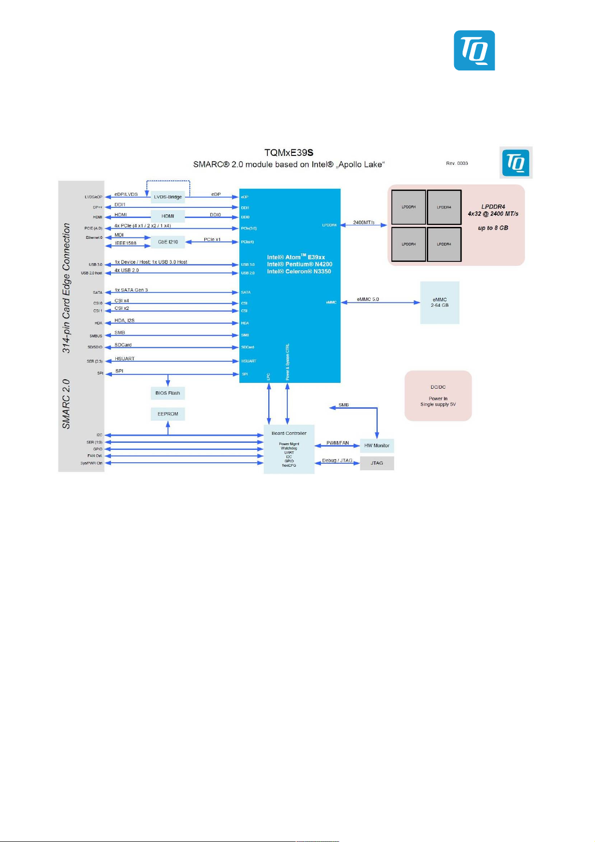
3.1 Block Diagram
The following illustration shows the block diagram of the TQMxE39S:
Illustration 1: Block Diagram TQMxE39S
3.2 Electrical Characteristics
3.2.1 Supply Voltage Characteristics
The TQMxE39S supports an input voltage from 4.75 V to 5.25 V.
The following supply voltages are specified at the SMARC connector:
• Main Power Rail: 4.75 V to 5.25 V max input ripple: ±100 mV
• VCC_RTC: 2.0 V to 3.3 V max input ripple: ±20 mV
The input voltages shall rise from 10 % of nominal to 90 % of nominal within 0.1 ms to 20 ms (0.1 ms ≤ Rise Time ≤ 20 ms).
There must be a smooth and continuous ramp of each DC output voltage from 10 % to 90 % of its final set point within the
regulation band.
User's Manual l TQMxE39S UM 0101 l © 2019 TQ-Group Page 7
3.2.2 Power Consumption
The values below show voltage and power consumption details for the TQMxE39S.
The values were measured using the TQMxE39S and the MB-SMARC-1 carrier board.
The measurement was done with two power supplies, one for the TQMxE39S and the other one for the MB-SMARC-1 carrier
board.
The power consumption of each TQMxE39S was measured running Windows® 10, 64 bit and a four chip LPDDR4 configuration (4
× 2 Gbyte). All measurements were done at a temperature of +25 °C and an input voltage of +5.0 V.
The power consumption of the TQMxE39S depends on the application, the mode of operation and the operating system.
The power consumption was measured under the following conditions:
• Suspend mode:
The system is in S5/S4 state, Ethernet port is disconnected.
• Windows 10, 64 bit, idle:
Desktop idles, Ethernet port is disconnected.
• Windows 10, 64 bit, maximum load:
These values show the maximum worst case power consumption, achieved by using the Intel® stress test tool to apply
maximum load to the cores only, and cores plus graphics engine, Ethernet port is connected (1000 Mbps Speed)
• Windows 10, 64 bit, Suspend Mode:
The system is in S5/S4 state, Ethernet port is disconnected.
The following table shows the power consumption with different CPU configurations.
Table 3: TQMxE39S Power Consumption
Module
Suspend (OS shut down) Win10, 64 bit idle Win10, 64 bit max. load
Mode
Intel® Pentium® N4200 0.33 W 2 W TBD
Intel® Celeron® N3350 0.33 W 2 W TBD
E3930 with 8 Gbyte LPDDR4 0.33 W 2 W 8 W
E3940 with 8 Gbyte LPDDR4 0.33 W 2 W 11.5 W
E3950 with 8 Gbyte LPDDR4 0.33 W 2 W 16 W
Note: Power requirement
The power supplies on the carrier board for the TQMxE39S must be designed with enough reserve.
The carrier board should provide at least twice the maximum workload power of the TQMxE39S.
The TQMxE39S supports several low-power states. The power supply of the carrier board has to be
stable even with no load.
User's Manual l TQMxE39S UM 0101 l © 2019 TQ-Group Page 8
3.2.2.1 Real Time Clock
The RTC (VCC_RTC) current consumption is shown below.
The values were measured at +25 °C under battery operating conditions.
Table 4: RTC Current Consumption
Integrated RTC Voltage Current
®
Intel
Atom™ E3900, Intel
®
Pentium® N4200, Intel® Celeron® N3350 3.0 V 3 μA
The current consumption of the RTC in the Intel
®
Atom™ E3900, Intel
®
Pentium® N4200, and Intel® Celeron® N3350
is specified in the Product Family Datasheet with 6 µA in average, but the values measured on several modules were lower.
3.3 Environment
• Operating Temperature Standard: 0 °C to +60 °C
• Operating Temperature Extended: –40 °C to +85 °C
• Storage Temperature: –40 °C to +85 °C
• Relative humidity (operating / storage): 10 % to 90 % (non-condensing)
Attention: Maximum operating temperature
Do not operate the TQMxE39S without heat spreader or without heat sink!
The heat spreader is not a sufficient heat sink!

User's Manual l TQMxE39S UM 0101 l © 2019 TQ-Group Page 9
3.4 System Components
3.4.1 CPU
The TQMxE39S supports the Intel
®
Atom™ E3900, Intel
®
Pentium® N4200, and Intel® Celeron® N3350 CPUs.
The following list shows some key features of these CPUs:
• Quad and dual CPU cores
• Intel
• Intel
• Intel
• Intel
• 2 Mbyte Cache
• Intel
®
64 Architecture
®
Virtualization Technology (VT-x)
®
Streaming SIMD Extensions 4.2 (Intel® SSE4.2)
®
Enhanced Intel® SpeedStep® technology
®
HD Graphics
• Triple independent displays
Table 5: Intel
Mode N3350 N4200 x5-E3930 x5-E3940 x7-E3950
CPU Cores 2 4 2 4 4
Cache 2 Mbyte 2 Mbyte 2 Mbyte 2 Mbyte 2 Mbyte
CPU frequency HFM / Turbo 1.1 / 2.4 GHz 1.1 / 2.5 GHz 1.3 / 1.8 GHz 1.6 / 1.8 GHz 1.6 / 2.0 GHz
Temperature T
Memory Speed 2400 MT/s 2400 MT/s 2133 MT/s 2133 MT/s 2400 MT/s
Max Memory 8 Gbyte 8 Gbyte 8 Gbyte 8 Gbyte 8 Gbyte
Max Memory Channels 4 x 32 4 x 32 4 x 32 4 x 32 4 x 32
®
Intel
HD Graphics Gen 9 500 505 500 500 505
GFX: No. of Execution Units 12 18 12 12 18
GFX: Base / Burst 200 / 650 MHz 200 / 750 MHz 400 / 550 MHz 400 / 600 MHz 500 / 650 MHz
Thermal Design Power (TDP) 6 W 6 W 6.5 W 9.5 W 12 W
junction
®
Atom™ E3900, Intel
0 °C to +105 °C 0 °C to +105 °C –40 °C to +110 °C –40 °C to +110 °C –40 °C to +110 °C
®
Pentium® N4200, and Intel® Celeron® N3350
3.4.2 Graphics
The Intel
®
Atom™ E3900, Intel
®
Pentium® N4200, and Intel® Celeron® N3350 CPUs includes an integrated Intel® HD (Gen 9)
graphics accelerator. It provides excellent 2D/3D graphics performance with dual simultaneous display support.
The following list shows some key features of the Intel
®
Atom™ E3900, Intel
®
Pentium® N4200, and Intel® Celeron® N3350 CPUs:
• Graphics Technology (Gen 09 LP) with 12 Execution Units (HD Graphics 500) or 18 Execution Units (HD Graphics 505)
• Hardware accelerated video decoding/encoding for H.264, MPEG2, MVC, VC-1, WMV9, H.265/HEVC, VP9, JPEG/MJPAG
• Direct3D* 12, DirectX* 12 support
• OpenGL* 4.3, OpenCL* 1.2 support
The TQMxE39S supports one Digital Display Interface (DDI) one HDMI interface and one eDP or LVDS interface at the SMARC
connector.
Table 6: Maximum Resolution in Dual Display Configuration
Display Maximum Display Resolution
LVDS 1920 × 1200 @ 60 Hz (dual channel)
eDP 3840 × 2160 @ 60 Hz
DP 4096 × 2160 @ 60 Hz
HDMI 3840 × 2160 @ 30 Hz

User's Manual l TQMxE39S UM 0101 l © 2019 TQ-Group Page 10
3.4.3 Memory
3.4.3.1 LPDDR4 SDRAM
The TQMxE39S supports a memory-down configuration running at up to 2400 MT/s.
The maximum memory size is 8 Gbyte. The available memory configuration can be 2 Gbyte, 4 Gbyte or 8 Gbyte.
3.4.3.2 eMMC
The TQMxE39S supports up to 64 Gbyte on-board eMMC 5.0 flash (compatible with rev. 5.0).
Attention: eMMC OS installation
The on-board eMMC Flash requires pre-configuration via EFI Shell before OS installation
(e.g. diskpart utility)
3.4.3.3 SPI Boot Flash
The TQMxE39S provides a 128 Mbit SPI boot flash. It includes the Intel® Trusted Execution Engine and the uEFI BIOS.
An external SPI boot flash can be used instead of the on-board SPI boot flash.
The uEFI BIOS supports the following 1.8 V SPI flash devices on the carrier board:
Winbond W25Q128FW / GigaDevice GD25LQ128D
Ensure that the QE (Quad Enable) bit is 0. Otherwise the SPI boot flash won’t work.
3.4.3.4 EEPROM
On the TQMxE39S there can be placed a 32 kbit serial EEPROM on the I2C_GP bus. This feature is optional.
3.4.4 Real Time Clock
The TQMxE39S includes a standard RTC (Motorola MC146818B) integrated in the Intel
®
Atom™ E3900, Intel
®
Pentium® N4200
and Intel® Celeron® N3350 CPU.
3.4.5 Hardware Monitor
The TQMxE39S includes an integrated Hardware Monitor to monitor the on-board temperature, board voltages and manage a
fan (GPIO5 / PWM_OUT and GPIO6 / TACHIN).
3.4.6 TQ flexible I/O configuration (TQ-flexiCFG)
The module includes a flexible I/O configuration feature, the TQ-flexiCFG.
Using the TQ-flexiCFG feature several I/O interfaces and functions can be configured via a programmable FPGA.
This feature enables the user to integrate special embedded features and configuration options in the TQMxE39S to reduce the
carrier board design effort. Here are some examples of the flexible I/O configuration:
• GPIO interrupt configuration
• Interrupt configuration via LPC Serial IRQ
• Serial Port handshake signals via GPIOs
• Integrate additional I/O functions, e.g. additional Serial, I
2
C, PWM controller or special power management
configurations
Please contact
support@tq-group.com for further information about the TQ-flexiCFG.

User's Manual l TQMxE39S UM 0101 l © 2019 TQ-Group Page 11
3.5 Interfaces
3.5.1 PCI Express
The TQMxE39S with Intel
®
Atom™ E3900, Intel
®
Pentium® N4200, and Intel® Celeron® N3350 CPU supports a very flexible
PCI Express configuration with up 4 PCI Express Gen 2 ports.
With a customized BIOS the PCI Express lanes can be configured as follows:
Table 7: PCI Express Configuration Options
SMARC Port 0 – 3 On-board Ethernet i210 Configuration
4 × 1 ports (maximum 3 ports enabled) enabled Configuration in the BIOS
4 × 1 ports disabled Configuration in the BIOS
2 × 2 ports enabled Configuration via custom BIOS
1 × 4 port enabled Configuration via custom BIOS
3.5.2 Gigabit Ethernet
The TQMxE39S provides the Intel® i210IT Ethernet controller with 10/100/1000 Mbps speed and IEEE1588 support.
3.5.3 Serial ATA
The TQMxE39S supports one SATA Gen 3.0 interface which supports up to 6 Gb/s.
The integrated SATA host controller supports AHCI mode, the SATA controller no longer supports legacy IDE mode using I/O
space.
3.5.4 Digital Display Interface
The TQMxE39S supports three Digital Display Interfaces: DisplayPort, HDMI and Embedded DisplayPort (eDP)
The module either supports eDP or LVDS (assembly option).
The TQMxE39S supports the following maximum display resolutions:
• DisplayPort 1.2a: Up to 4096 × 2160 @ 60 Hz
• Embedded DisplayPort 1.3: Up to 3840 × 2160 @ 60 Hz
• HDMI 1.4b: Up to 3840 × 2160 @ 30 Hz
• DVI: Up to 3840 × 2160 @ 30 Hz (HDMI without Audio)
Please contact
support@tq-group.com for further information about the display configuration.
3.5.5 LVDS Interface
The TQMxE39S supports an LVDS interface which is provided through an on-board eDP to LVDS bridge.
The eDP to LVDS bridge supports single or dual LVDS signalling with colour depths of 18 bits per pixel or 24 bits per pixel up to
112 MHz and a resolution up to 1920 × 1200 @ 60 Hz in dual LVDS mode. The LVDS data packing can be configured either in
VESA or JEIDA format.
The eDP to LVDS bridge can emulate EDID ROM behaviour avoiding specific changes in system video BIOS, to support panels
without EDID ROM.
Please contact
support@tq-group.com for further information about the LVDS configuration.
User's Manual l TQMxE39S UM 0101 l © 2019 TQ-Group Page 12
3.5.6 USB 2.0 Interfaces
The TQMxE39S supports six USB 2.0 ports at the SMARC connector.
3.5.7 USB 3.0 Interfaces
The TQMxE39S supports two USB 3.0 ports at the SMARC connector.
Note: USB Port Mapping
The USB 2.0 port 0 must be paired with USB 3.0 SuperSpeed port 0.
The USB 2.0 port 1 must be paired with USB 3.0 SuperSpeed port 1.
3.5.8 SD Card Interface
The TQMxE39S provides an SD card interface for 4-bit SD/MMC cards at the SMARC connector.
3.5.9 General Purpose Input/Output
The TQMxE39S provides twelve GPIO signals at the SMARC connector.
The GPIO signals are shared with camera control, fan Control and HD Audio Reset signals. They can be configured by software.
The GPIO signals are integrated in the TQ-flexiCFG block and can be configured flexible.
Therefore the signals can also be used for several special functionality (see 3.4.6).
Please contact
support@tq-group.com for further information about the GPIO configuration and their alternate uses.
3.5.10 Audio Interface
The TQMxE39S provides a High Definition Audio (I) and an I2 interface, which support Audio codecs at the SMARC connector. The
audio codec on the carrier board should be supported by the BIOS of the TQMxE39S.
Please contact
support@tq-group.com for further information.
3.5.11 MIPI CSI Camera Interface
The TQMxE39S supports two camera interfaces where 2- or 4-lane MIPI CSI cameras can be connected.
3.5.12 I
2
C Bus
The TQMxE39S supports a general purpose I2C bus via a dedicated LPC to I2C controller, integrated in the TQ-flexiCFG block.
The I2C host controller supports a clock frequency of up to 400 kHz and can be configured independently.
3.5.13 SMBus / Power Management I
2
C Bus
The TQMxE39S provides an I2C based SMBus interface. This bus is also called power management I2C bus.
3.5.14 Serial Peripheral Interface
The TQMxE39S provides an SPI interface. The SPI interface can only be used for SPI boot Flash devices.

User's Manual l TQMxE39S UM 0101 l © 2019 TQ-Group Page 13
3.5.15 Serial Ports
The TQMxE39S offers up to four UARTs (Universal Asynchronous Receiver and Transmitter). The register set of SER0 and SER1 is
based on the industry standard 16550 UART. The UART operates with standard serial port drivers without requiring a custom
driver to be installed. The 16 byte transmit and receive FIFOs reduce CPU overhead and minimize the risk of buffer overflow and
data loss.
SER2 and SER3 are connected to the HSUART (High Speed UART) of the Intel
®
Atom™ E3900, Intel
®
Pentium® N4200, or
Intel® Celeron® N3350 CPU.
TQ recommends preferring the usage of SER0 and SER1. There might be some problems with serial console when using the
Intel® HSUARTs.
3.5.16 Watchdog Timer
The TQMxE39S supports a freely programmable two-stage Watchdog timer, integrated in the TQ-flexiCFG block.
There are four operation modes available for the Watchdog timer:
• Dual-stage mode
• Interrupt mode
• Reset mode
• Timer mode
The timeout of the Watchdog timer ranges from 125 msec to 1 h.
The SMARC Specification does not support external hardware triggering of the Watchdog.
An external Watchdog Trigger can be configured to GPIO pins at the SMARC connector with the TQ-flexiCFG feature.
3.6 Connectors
3.6.1 SMARC Connector
A 314 pin 0.5 mm pitch card edge connector is realized on the TQMxE39S PCB. On the carrier board a connector mechanical
compatible to MXM3 graphic cards is used to contact the module. The stacking height is defined by the connector used on the
carrier (e.g. 1.5 mm, 2.7 mm, 5 mm, and 8 mm are available).
3.6.2 TQM Debug Card
The TQM debug card is designed to provide access to several processor and chipset control signals. The uEFI BIOS Power-On SelfTest (POST) codes can be displayed through four hexadecimal display panels on the TQM debug card.
When the module is turned on, the hexadecimal display should show the uEFI BIOS POST codes. If the module does not boot, the
uEFI BIOS POST has detected a fatal fault and stopped. The number showing in the hexadecimal display on the TQM debug card
is the number of the test in which uEFI BIOS boot failed.
The debug card can be connected with an adaptor PCB in combination with the MB-SMARC-1.
Illustration 2: TQM Debug Card

User's Manual l TQMxE39S UM 0101 l © 2019 TQ-Group Page 14
3.6.3 Debug Module LED
The TQMxE39S includes a dual colour LED providing boot and BIOS information.
The following table shows some LED boot messages.
Table 8: LED Boot Messages
Red LED Green LED Remark
ON OFF Power supply error
ON ON S4/S5 state
BLINKING BLINKING S3 state
OFF BLINKING uEFI BIOS is booting
OFF ON uEFI BIOS boot is finished
3.7 SMARC Connector Pinout List
This section describes the TQMxE39S SMARC connector pin assignment, which is compliant with the SMARC hardware
specification Version 2.0.
3.7.1 Signal Assignment Abbreviations
Table 9 lists the abbreviations used in Table 10.
Table 9: Abbreviations used
Abbreviation Description
GND Ground
PWR Power
I Input
I PU Input with pull-up resistor
I PD Input with pull-down resistor
O Output
OD Open drain output
IO Bi-directional
Note: Unused signals on the carrier board
If the input signals at the SMARC connector are not used, these signals can be left open on the carrier
board, since these signals have a termination on the TQMxE39S.

User's Manual l TQMxE39S UM 0101 l © 2019 TQ-Group Page 15
3.7.2 SMARC Connector Pin Assignment
Table 10: SMARC Connector Pin Assignment
Pin Pin-Signal Description Type Level Remark
P1 SMB_ALERT_1V8# SM Bus Alert# (interrupt) signal I PU 1.8 V
P2 GND Ground GND
P3 CSI1_CK+ CSI differential clock inputs I LVDS D-PHY
P4 CSI1_CK– CSI differential clock inputs I LVDS D-PHY
P5 GBE1_SDP IEEE 1588 Trigger Signal IO 3.3 V N/A
P6 GBE0_SDP IEEE 1588 Trigger Signal IO 3.3 V
P7 CSI1_RX0+ CSI differential data inputs I LVDS D-PHY
P8 CSI1_RX0– CSI differential data inputs I LVDS D-PHY
P9 GND Ground GND
P10 CSI1_RX1+ CSI differential data inputs I LVDS D-PHY
P11 CSI1_RX1– CSI differential data inputs I LVDS D-PHY
P12 GND Ground GND
P13 CSI1_RX2+ CSI differential data inputs I LVDS D-PHY
P14 CSI1_RX2– CSI differential data inputs I LVDS D-PHY
P15 GND Ground GND
P16 CSI1_RX3+ CSI differential data inputs I LVDS D-PHY
P17 CSI1_RX3– CSI differential data inputs I LVDS D-PHY
P18 GND Ground GND
P19 GBE0_MDI3– Gigabit Ethernet Controller: Media Dependent Interface IO GBE MDI
P20 GBE0_MDI3+ Gigabit Ethernet Controller: Media Dependent Interface IO GBE MDI
P21 GBE0_LINK100# Link Speed Indication LED for 100 Mbps OD 3.3 V tolerant
P22 GBE0_LINK1000# Link Speed Indication LED for 1000 Mbps OD 3.3 V tolerant
P23 GBE0_MDI2– Gigabit Ethernet Controller: Media Dependent Interface IO GBE MDI
P24 GBE0_MDI2+ Gigabit Ethernet Controller: Media Dependent Interface IO GBE MDI
P25 GBE0_LINK_ACT# Link / Activity Indication LED OD 3.3 V tolerant
P26 GBE0_MDI1– Gigabit Ethernet Controller: Media Dependent Interface IO GBE MDI
P27 GBE0_MDI1+ Gigabit Ethernet Controller: Media Dependent Interface IO GBE MDI
P28 GBE0_CTREF Center-Tap reference voltage for Carrier Ethernet magnetics PWR
P29 GBE0_MDI0– Gigabit Ethernet Controller: Media Dependent Interface IO GBE MDI
P30 GBE0_MDI0+ Gigabit Ethernet Controller: Media Dependent Interface IO GBE MDI
P31 SPI0_CS1# SPI0 Master Chip Select 1 output O 1.8 V
P32 GND Ground GND
P33 SDIO_WP SD Card: Write Protect I 3.3 V
P34 SDIO_CMD SD Card: Command line IO 3.3 V
P35 SDIO_CD# SD Card: Card Detect I 3.3 V
P36 SDIO_CK SD Card: Clock O 3.3 V
P37 SDIO_PWR_EN SD Card: Power enable O (PU) 3.3 V PU to 3.3 V
P38 GND Ground GND
P39 SDIO_D0 SD Card: data path IO 3.3 V
P40 SDIO_D1 SD Card: data path IO 3.3 V
P41 SDIO_D2 SD Card: data path IO 3.3 V
P42 SDIO_D3 SD Card: data path IO 3.3 V
P43 SPI0_CS0# SPI0 Master Chip Select 0 output O 1.8 V
P44 SPI0_CK SPI0 Master Clock output O 1.8 V
P45 SPI0_DIN SPI0 Master Data input (CPU input, SPI device output) I 1.8 V
P46 SPI0_DO SPI0 Master Data output (CPU output, SPI device input) O 1.8 V
P47 GND Ground GND
P48 SATA_TX+ Differential SATA transmit data Pair O SATA
P49 SATA_TX– Differential SATA transmit data Pair O SATA
P50 GND Ground GND
P51 SATA_RX+ Differential SATA receive data Pair I SATA
P52 SATA_RX– Differential SATA receive data Pair I SATA

User's Manual l TQMxE39S UM 0101 l © 2019 TQ-Group Page 16
Table 10: SMARC Connector Pin Assignment (continued)
Pin Pin-Signal Description Type Level Remark
P53 GND Ground GND
P54 ESPI_CS0# LPSS SPI: Slave select O 1.8 V
P55 ESPI_CS1# LPSS SPI: Slave select O 1.8 V
P56 ESPI_CK LPSS SPI: Clock signal O 1.8 V
P57 ESPI_IO_1 LPSS SPI: RXD (MISO) I or IO 1.8 V
P58 ESPI_IO_0 LPSS SPI: TXD (MOSI) O or IO 1.8 V
P59 GND Ground GND
P60 USB0+ USB differential pair IO USB
P61 USB0– USB differential pair IO USB
P62 USB0_EN_OC# USB over-current input / enable output (both OD) IO PU 3.3 V OD input only 1
P63 USB0_VBUS_DET Host power detection (when port is used as device) I PD 5 V N/A
P64 USB0_OTG_ID USB OTG ID input, active high (high device) I PU 3.3 V N/A
P65 USB1+ USB differential pair IO USB
P66 USB1– USB differential pair IO USB
P67 USB1_EN_OC# USB over-current input / enable output (both OD) IO PU 3.3 V
OD input only 1
P68 GND Ground GND
P69 USB2+ USB differential pair IO USB
P70 USB2– USB differential pair IO USB
P71 USB2_EN_OC# USB over-current input / enable output (both OD) IO PU 3.3 V
OD input only 1
P72 RSVD Reserved
P73 RSVD Reserved
P74 USB3_EN_OC# USB over-current input / enable output (both OD) IO PU 3.3 V
P75 PCIE_A_RST# PCIe Port reset output O 3.3 V
P76 USB4_EN_OC# USB over-current input / enable output (both OD) IO PU 3.3 V
OD input only 1
1
OD input only 1
P77 RSVD Reserved
P78 RSVD Reserved
P79 GND Ground GND
P80 PCIE_C_REFCK+ Differential PCIe Link reference clock output O PCIe
P81 PCIE_C_REFCK– Differential PCIe Link reference clock output O PCIe
P82 GND Ground GND
P83 PCIE_A_REFCK+ Differential PCIe Link reference clock output O PCIe
P84 PCIE_A_REFCK– Differential PCIe Link reference clock output O PCIe
P85 GND Ground GND
P86 PCIE_A_RX+ Differential PCIe Link receive data pair I PCIe
P87 PCIE_A_RX– Differential PCIe Link receive data pair I PCIe
P88 GND Ground GND
P89 PCIE_A_TX+ Differential PCIe Link transmit data pair O PCIe
P90 PCIE_A_TX– Differential PCIe Link transmit data pair O PCIe
P91 GND Ground GND
P92 HDMI_D2+ / DP1_LANE0+ TMDS / HDMI data differential pair / DP data pair O TDMS / DP HDMI only
P93 HDMI_D2– / DP1_LANE0– TMDS / HDMI data differential pair / DP data pair O TDMS / DP HDMI only
P94 GND Ground GND
P95 HDMI_D1+ / DP1_LANE1+ TMDS / HDMI data differential pair / DP data pair O TDMS / DP HDMI only
P96 HDMI_D1– / DP1_LANE1– TMDS / HDMI data differential pair / DP data pair O TDMS / DP HDMI only
P97 GND Ground GND
P98 HDMI_D0+ / DP1_LANE2+ TMDS / HDMI data differential pair / DP data pair O TDMS / DP HDMI only
P99 HDMI_D0– / DP1_LANE2– TMDS / HDMI data differential pair / DP data pair O TDMS / DP HDMI only
P100 GND Ground GND
P101 HDMI_CK+ / DP1_LANE3+ HDMI differential clock output pair / DP data pair O TDMS / DP HDMI only
P102 HDMI_CK– / DP1_LANE3– HDMI differential clock output pair / DP data pair O TDMS / DP HDMI only
P103 GND Ground GND
P104 HDMI_HPD / DP1_HPD HDMI / DP Hot Plug Detect input I PD 1.8 V HDMI only PD
1: Configurable through TQ-flexiCFG.

User's Manual l TQMxE39S UM 0101 l © 2019 TQ-Group Page 17
Table 10: SMARC Connector Pin Assignment (continued)
Pin Pin-Signal Description Type Level Remark
P105 HDMI_CTRL_CK / DP1_AUX+ HDMI I2C clock / DP AUX Channel O / IO 1.8 V / DP HDMI only; PU
P106 HDMI_CTRL_DAT / DP1_AUX– HDMI I2C data / DP AUX Channel IO 1.8 V / DP HDMI only; PU
P107 DP1_AUX_SEL
P108 GPIO0 / CAM0_PWR#
P109 GPIO1 / CAM1_PWR#
P110 GPIO2 / CAM0_RST# GPIO / Camera reset (active low output) IO PU/O 1.8 V
P111 GPIO3 / CAM1_RST# GPIO / Camera reset (active low output) IO PU/O 1.8 V
P112 GPIO4 / HDA_RST# GPIO / HD audio reset (active low output) IO PU/O 1.8 V
P113 GPIO5 / PWM_OUT GPIO / PWM out for fan speed control IO PU/O 1.8 V
P114 GPIO6 / TACHIN
P115 GPIO7 GPIO IO PU 1.8 V
P116 GPIO8 GPIO IO PU 1.8 V
P117 GPIO9 GPIO IO PU 1.8 V
P118 GPIO10 GPIO IO PU 1.8 V
P119 GPIO11 GPIO IO PU 1.8 V
P120 GND Ground GND
P121 I2C_PM_CK Power management I2C bus: SMBus IO PU 1.8 V
P122 I2C_PM_DAT Power management I2C bus: SMBus IO PU 1.8 V
P123 BOOT_SEL0# Boot source select I 1.8 V N/A
P124 BOOT_SEL1# Boot source select I 1.8 V N/A
P125 BOOT_SEL2#
P126 RESET_OUT# General purpose reset output to carrier board O 1.8 V
P127 RESET_IN# Reset input from Carrier board I PU 1.8 V
P128 POWER_BTN# Power-button input from Carrier board I PU 1.8 V
P129 SER0_TX Serial port data out O 1.8 V
P130 SER0_RX Serial port data in I 1.8 V
P131 SER0_RTS# Serial port handshake: Request to Send O 1.8 V
P132 SER0_CTS# Serial port handshake: Clear to Send I 1.8 V
P133 GND Ground GND
P134 SER1_TX Serial port data out O 1.8 V
P135 SER1_RX Serial port data in I 1.8 V
P136 SER2_TX Serial port data out O 1.8 V
P137 SER2_RX Serial port data in I 1.8 V
P138 SER2_RTS# Serial port handshake: Request to Send O 1.8 V
P139 SER2_CTS# Serial port handshake: Clear to Send I 1.8 V
P140 SER3_TX Serial port data out O 1.8 V
P141 SER3_RX Serial port data in I 1.8 V
P142 GND Ground GND
P143 CAN0_TX CAN Transmit output O 1.8 V N/A
P144 CAN0_RX CAN Receive input I 1.8 V N/A
P145 CAN1_TX CAN Transmit output O 1.8 V N/A
P146 CAN1_RX CAN Receive input I 1.8 V N/A
P147 VDD_IN Module power input voltage PWR 4.75 to 5.25 V
P148 VDD_IN Module power input voltage PWR 4.75 to 5.25 V
P149 VDD_IN Module power input voltage PWR 4.75 to 5.25 V
P150 VDD_IN Module power input voltage PWR 4.75 to 5.25 V
P151 VDD_IN Module power input voltage PWR 4.75 to 5.25 V
P152 VDD_IN Module power input voltage PWR 4.75 to 5.25 V
P153 VDD_IN Module power input voltage PWR 4.75 to 5.25 V
P154 VDD_IN Module power input voltage PWR 4.75 to 5.25 V
P155 VDD_IN Module power input voltage PWR 4.75 to 5.25 V
P156 VDD_IN Module power input voltage PWR 4.75 to 5.25 V
DP AUX select (to select between DP and HDMI)
GPIO / Camera power enable (active low output)
GPIO / Camera power enable (active low output)
GPIO / Tachometer input for fan speed measurement
Boot source select (tie to GND to boot from carrier SPI)
I 1.8 V N/A
IO PU/O 1.8 V
IO PU/O 1.8 V
IO PU/O 1.8 V
I PU 1.8 V
2
2
2
2
Preconfigured to HDA_RST#
Preconfigured to PWM_OUT
Preconfigured to TACHIN
2
2
2
2
2
2
2
2
2
2
2
2
2
2
2
2
2
2
2: Configurable through TQ-flexiCFG.

User's Manual l TQMxE39S UM 0101 l © 2019 TQ-Group Page 18
Table 10: SMARC Connector Pin Assignment (continued)
Pin Pin-Signal Description Type Level Remark
S1 CSI1_TX+ / I2C_CAM1_CK Camera configurations differential data / Camera I2C O/IO PU TDMS / 1.8 V I2C only
S2 CSI1_TX– / I2C_CAM1_DAT Camera configurations differential data / Camera I2C O/IO PU TDMS / 1.8 V I2C only
S3 GND Ground GND
S4 RSVD Reserved
3
S5 CSI0_TX+ / I2C_CAM0_CK Camera configurations differential data / Camera I2C O/IO PU TDMS / 1.8 V I2C only
S6 CAM_MCK Master clock output for CSI camera support O 1.8 V
S7 CSI0_TX– / I2C_CAM0_DAT Camera configurations differential data / Camera I2C O/IO PU TDMS / 1.8 V I2C only
S8 CSI0_CK+ CSI differential clock inputs I LVDS D-PHY
S9 CSI0_CK– CSI differential clock inputs I LVDS D-PHY
S10 GND Ground GND
S11 CSI0_RX0+ CSI differential data inputs I LVDS D-PHY
S12 CSI0_RX0– CSI differential data inputs I LVDS D-PHY
S13 GND Ground GND
S14 CSI0_RX1+ CSI differential data inputs I LVDS D-PHY
S15 CSI0_RX1– CSI differential data inputs I LVDS D-PHY
S16 GND Ground GND
S17 GBE1_MDI0+ Gigabit Ethernet Controller: Media Dependent Interface IO GBE MDI N/A
S18 GBE1_MDI0– Gigabit Ethernet Controller: Media Dependent Interface IO GBE MDI N/A
S19 GBE1_LINK100# Link Speed Indication LED for 100 Mbps OD 3.3 V tolerant N/A
S20 GBE1_MDI1+ Gigabit Ethernet Controller: Media Dependent Interface IO GBE MDI N/A
S21 GBE1_MDI1– Gigabit Ethernet Controller: Media Dependent Interface IO GBE MDI N/A
S22 GBE1_LINK1000# Link Speed Indication LED for 1000 Mbps OD 3.3 V tolerant N/A
S23 GBE1_MDI2+ Gigabit Ethernet Controller: Media Dependent Interface IO GBE MDI N/A
S24 GBE1_MDI2– Gigabit Ethernet Controller: Media Dependent Interface IO GBE MDI N/A
S25 GND Ground GND
S26 GBE1_MDI3+ Gigabit Ethernet Controller: Media Dependent Interface IO GBE MDI N/A
S27 GBE1_MDI3– Gigabit Ethernet Controller: Media Dependent Interface IO GBE MDI N/A
S28 GBE1_CTREF Center-Tap reference voltage for Carrier Ethernet magnetics PWR N/A
S29 PCIE_D_TX+ Differential PCIe Link transmit data pair O PCIe
S30 PCIE_D_TX– Differential PCIe Link transmit data pair O PCIe
S31 GBE1_LINK_ACT# Link / Activity Indication LED OD 3.3 V tolerant N/A
S32 PCIE_D_RX+ Differential PCIe Link receive data pair I PCIe
S33 PCIE_D_RX– Differential PCIe Link receive data pair I PCIe
S34 GND Ground GND
S35 USB4+ USB differential pair IO USB
S36 USB4– USB differential pair IO USB
S37 USB3_VBUS_DET Host power detection (when port is used as device) I PD 5 V
S38 AUDIO_MCK I2S: Master clock output to Audio codecs O 1.8 V
S39 I2S0_LRCK I2S: Left& Right audio synchronization clock IO 1.8 V
S40 I2S0_SDOUT I2S: Digital audio Output O 1.8 V
S41 I2S0_SDIN I2S: Digital audio Input I 1.8 V
S42 I2S0_CK I2S: Digital audio clock IO 1.8 V
S43 ESPI_ALERT0# Input from eSPI slave to request service from master I 1.8 V N/A
S44 ESPI_ALERT1# Input from eSPI slave to request service from master I 1.8 V N/A
S45 RSVD Reserved
3
S46 RSVD Reserved
S47 GND Ground GND
S48 I2C_GP_CK General Purpose I2C bus IO PU 1.8 V
S49 I2C_GP_DAT General Purpose I2C bus IO PU 1.8 V
S50 HDA_SYNC / I2S2_LRCK HDA: sync / I2S: Left& Right audio synchronization clock IO 1.8 V
S51 HDA_SDO / I2S2_SDOUT HDA: data out / / I2S: Digital audio Output O 1.8 V
S52 HDA_SDI / I2S2_SDIN HDA: data in / I2S: Digital audio Input I 1.8 V
3: Configurable through TQ-flexiCFG.

User's Manual l TQMxE39S UM 0101 l © 2019 TQ-Group Page 19
Table 10: SMARC Connector Pin Assignment (continued)
Pin Pin-Signal Description Type Level Remark
S53 HDA_CK / I2S2_CK HDA: clock / I2S: Digital audio clock IO 1.8 V
S54 SATA_ACT# Active low SATA activity indicator (16 mA max) OD 3.3 V
S55 USB5_EN_OC# USB over-current input / enable output (both OD) IO PU 3.3 V
4
OD input only 4
S56 ESPI_IO_2 ESPI Master Data Input / Outputs IO 1.8 V N/A
S57 ESPI_IO_3 ESPI Master Data Input / Outputs IO 1.8 V N/A
S58 ESPI_RESET# ESPI Reset O 1.8 V
S59 USB5+ USB differential pair IO USB
S60 USB5– USB differential pair IO USB
S61 GND Ground GND
S62 USB3_SSTX+ Differential USB SuperSpeed transmit data pair O USB SS
S63 USB3_SSTX– Differential USB SuperSpeed transmit data pair O USB SS
S64 GND Ground GND
S65 USB3_SSRX+ Differential USB SuperSpeed receive data pair I USB SS
S66 USB3_SSRX– Differential USB SuperSpeed receive data pair I USB SS
S67 GND Ground GND
S68 USB3+ USB differential pair IO USB
S69 USB3– USB differential pair IO USB
S70 GND Ground GND
S71 USB2_SSTX+ Differential USB SuperSpeed transmit data pair O USB SS
S72 USB2_SSTX– Differential USB SuperSpeed transmit data pair O USB SS
S73 GND Ground GND
S74 USB2_SSRX+ Differential USB SuperSpeed receive data pair I USB SS
S75 USB2_SSRX– Differential USB SuperSpeed receive data pair I USB SS
S76 PCIE_B_RST# PCIe Port reset output O 3.3 V
S77 PCIE_C_RST# PCIe Port reset output O 3.3 V
S78 PCIE_C_RX+ Differential PCIe Link receive data pair I PCIe
S79 PCIE_C_RX– Differential PCIe Link receive data pair I PCIe
S80 GND Ground GND
S81 PCIE_C_TX+ Differential PCIe Link transmit data pair O PCIe
S82 PCIE_C_TX– Differential PCIe Link transmit data pair O PCIe
S83 GND Ground GND
S84 PCIE_B_REFCK+ Differential PCIe Link reference clock output O PCIe
S85 PCIE_B_REFCK– Differential PCIe Link reference clock output O PCIe
S86 GND Ground GND
S87 PCIE_B_RX+ Differential PCIe Link receive data pair I PCIe
S88 PCIE_B_RX– Differential PCIe Link receive data pair I PCIe
S89 GND Ground GND
S90 PCIE_B_TX+ Differential PCIe Link transmit data pair O PCIe
S91 PCIE_B_TX– Differential PCIe Link transmit data pair O PCIe
S92 GND Ground GND
S93 DP0_LANE0+ DP++ data differential pair O DP++
S94 DP0_LANE0– DP++ data differential pair O DP++
S95 DP0_AUX_SEL DP AUX select (to select between DP and HDMI) I PD 1.8 V PD
S96 DP0_LANE1+ DP++ data differential pair O DP++
S97 DP0_LANE1– DP++ data differential pair O DP++
S98 DP0_HPD DP++ Hot Plug Detect input I PD 1.8 V PD
S99 DP0_LANE2+ DP++ data differential pair O DP++
S100 DP0_LANE2– DP++ data differential pair O DP++
S101 GND Ground GND
S102 DP0_LANE3+ DP++ data differential pair O DP++
S103 DP0_LANE3– DP++ data differential pair O DP++
S104 USB3_OTG_ID USB OTG ID input, active high (high device) I PU 3.3 V
4: Configurable through TQ-flexiCFG.

User's Manual l TQMxE39S UM 0101 l © 2019 TQ-Group Page 20
Table 10: SMARC Connector Pin Assignment (continued)
Pin Pin-Signal Description Type Level Remark
S105 DP0_AUX+ DP++ AUX Channel (could also be used as 3.3 V I2C for HDMI) IO DP++ /3.3 V PU at high AUX_SEL
S106 DP0_AUX– DP++ AUX Channel (could also be used as 3.3 V I2C for HDMI) IO DP++ /3.3 V PU at high AUX_SEL
S107 LCD1_BKLT_EN LCD Backlight enable: high enables panel backlight O 1.8 V N/A
S108 LVDS1_CK+ / eDP1_AUX+ / DSI1_CLK+ LVDS LCD differential clock pair / eDP AUX Channel O/IO LVDS/DP LVDS only
S109 LVDS1_CK– / eDP1_AUX– / DSI1_CLK– LVDS LCD differential clock pair / eDP AUX Channel O/IO LVDS/DP LVDS only
S110 GND Ground GND
S111 LVDS1_0+ / eDP1_TX0+ / DSI1_D0+ LVDS / eDP data differential pair / O LVDS/DP LVDS only
S112 LVDS1_0– / eDP1_TX0– / DSI1_D0– LVDS / eDP data differential pair / O LVDS/DP LVDS only
S113 eDP1_HPD eDP Hot Plug Detect I PD 1.8 V N/A
S114 LVDS1_1+ / eDP1_TX1+ / DSI1_D1+ LVDS / eDP data differential pair / O LVDS/DP LVDS only
S115 LVDS1_1– / eDP1_TX1– / DSI1_D1– LVDS / eDP data differential pair / O LVDS/DP LVDS only
S116 LCD1_VDD_EN Enable signal for panel power O 1.8 V N/A
S117 LVDS1_2+ / eDP1_TX2+ / DSI1_D2+ LVDS / eDP data differential pair / O LVDS/DP LVDS only
S118 LVDS1_2– / eDP1_TX2– / DSI1_D2– LVDS / eDP data differential pair / O LVDS/DP LVDS only
S119 GND Ground GND
S120 LVDS1_3+ / eDP1_TX3+ / DSI1_D3+ LVDS / eDP data differential pair / O LVDS/DP LVDS only
S121 LVDS1_3– / eDP1_TX3– / DSI1_D3– LVDS / eDP data differential pair / O LVDS/DP LVDS only
S122 LCD1_BKLT_PWM Display Backlight brightness control output (PWM) O 1.8 V N/A
S123 RSVD Reserved
S124 GND Ground GND
S125 LVDS0_0+ / eDP0_TX0+ / DSI0_D0+ LVDS / eDP data differential pair / O LVDS/DP
S126 LVDS0_0– / eDP0_TX0– / DSI0_D0– LVDS / eDP data differential pair / O LVDS/DP
S127 LCD0_BKLT_EN LCD Backlight enable: high enables panel backlight O 1.8 V
S128 LVDS0_1+ / eDP0_TX1+ / DSI0_D1+ LVDS / eDP data differential pair / O LVDS/DP
S129 LVDS0_1– / eDP0_TX1– / DSI0_D1– LVDS / eDP data differential pair / O LVDS/DP
S130 GND Ground GND
S131 LVDS0_2+ / eDP0_TX2+ / DSI0_D2+ LVDS / eDP data differential pair / O LVDS/DP
S132 LVDS0_2– / eDP0_TX2– / DSI0_D2– LVDS / eDP data differential pair / O LVDS/DP
S133 LCD0_VDD_EN Enable signal for panel power O 1.8 V
S134 LVDS0_CK+ / eDP0_AUX+ / DSI0_CLK+ LVDS LCD differential clock pair / eDP AUX Channel O/IO LVDS/DP
S135 LVDS0_CK– / eDP0_AUX– / DSI0_CLK– LVDS LCD differential clock pair / eDP AUX Channel O/IO LVDS/DP
S136 GND Ground GND
S137 LVDS0_3+ / eDP0_TX3+ / DSI0_D3+ LVDS / eDP data differential pair / O LVDS/DP
S138 LVDS0_3– / eDP0_TX3– / DSI0_D3– LVDS / eDP data differential pair / O LVDS/DP
S139 I2C_LCD_CK I2C bus to read display EDID EEPROMs (for LVDS displays) IO PU 1.8 V
S140 I2C_LCD_DAT I2C bus to read display EDID EEPROMs (for LVDS displays) IO PU 1.8 V
S141 LCD0_BKLT_PWM Display Backlight brightness control output (PWM) O 1.8 V
S142 RSVD Reserved
S143 GND Ground GND
S144 eDP0_HPD eDP Hot Plug Detect I PD 1.8 V
S145 WDT_TIME_OUT# Watch-Dog-Timer Output O 1.8 V
S146 PCIE_WAKE# PCIe wake up interrupt to host I PU 3.3 V
S147 VDD_RTC Real-time clock circuit-power input PWR 2 V to 3.3 V
S148 LID# Lid open/close indication to module (low indicates closed lid) I PU 1.8 V
S149 SLEEP# Sleep indicator from carrier board I PU 1.8 V
S150 VIN_PWR_BAD# Power bad indication from Carrier board I PU VDD_IN
S151 CHARGING# Held low by carrier during battery charging I PU 1.8 V
S152 CHARGER_PRSNT# Held low by carrier if DC input for battery charger is present I PU 1.8 V
S153 CARRIER_STBY# Driven low by module during standby power state. (SUS_S3#) O 1.8 V
S154 CARRIER_PWR_ON Signal to carrier to turn on determined power supplies (SUS_S5#) O 1.8 V
S155 FORCE_RECOV# Force recovery input: pull low to load BIOS defaults I PU 1.8 V
S156 BATLOW# Battery low indication to module I PU 1.8 V
5
5
5
5
5
5
5
5
5
5: Configurable through TQ-flexiCFG.

User's Manual l TQMxE39S UM 0101 l © 2019 TQ-Group Page 21
4. MECHANICS
4.1 TQMxE39S Dimensions
The dimensions of the TQMxE39S are 82 mm × 50 mm.
The following illustration shows the Three View Drawing of the TQMxE39S.
Illustration 3: Three View Drawing TQMxE39S
The following illustration shows the bottom view of the TQMxE39S.
Illustration 4: Bottom View Drawing TQMxE39S

User's Manual l TQMxE39S UM 0101 l © 2019 TQ-Group Page 22
4.2 Heat Spreader Dimensions
The TQMxE39S supports two different heat spreader versions.
Both versions are compliant to the SMARC specification with 6 mm height.
Heat spreader for the Intel® Pentium® N4200, and Intel® Celeron® N3350 CPU
• TQMxE39S-HSP-N
Heat spreader for the Intel
®
Atom™ E3900 CPU
• TQMxE39S-HSP-E
The following illustration shows the standard heat spreader (TQMxE39S-HSP) for the TQMxE39S.
Illustration 5: Standard Heat Spreader TQMxE39S-HSP
Attention: Heat Spreader
The packages of the Intel® Pentium® N4200 and the Intel® Celeron® N3350 CPU have a different
height than the package of the Intel
The Intel
®
Atom™ E3900 CPU family includes an integrated heat spreader, the Intel
®
Atom™ E3900 CPU!
®
Pentium® N4200
and the Intel® Celeron® N3350 CPUs have no integrated heat spreaders.
Both CPU packages require different heat spreader versions. It is not permitted to use the
TQMxE39S-HSP-E heat spreader on the Intel® Pentium® N4200 or the Intel® Celeron® N3350 CPU.
It is also not permitted to use the TQMxE39S-HSP-N heat spreader on the Intel
®
Atom™ E3900 CPU.
To mount the wrong heat spreader will damage the TQMxE39S.
If a special cooling solution has to be implemented an extensive thermal design analysis and verification has to be performed.
TQ-Systems GmbH offers thermal analysis and simulation as a service.
Please contact
support@tq-group.com for more details about 2D/3D Step models.

User's Manual l TQMxE39S UM 0101 l © 2019 TQ-Group Page 23
4.3 Mechanical and Thermal Considerations
The TQMxE39S is designed to operate in a wide range of thermal environments.
An important factor for each system integration is the thermal design. The heat spreader acts as a thermal coupling device to the
TQMxE39S. The heat spreader is thermally coupled to the CPU: It provides optimal heat transfer from the TQMxE39S to the heat
spreader. The heat spreader itself is not an appropriate heat sink.
System designers can implement different passive and active cooling versions through the thermal connection to the heat
spreader.
Attention: Thermal Considerations
Do not operate the TQMxE39S without heat spreader or without heat sink!
The heat spreader is not a sufficient heat sink!
If a special cooling solution has to be implemented, an extensive thermal design analysis and verification has to be performed.
TQ-Systems GmbH offers thermal analysis and simulation as a service.
Please contact support@tq-group.com for more information about the thermal configuration.
4.4 Protection Against External Effects
The TQMxE39S itself is not protected against dust, external impact and contact (IP00).
Adequate protection has to be guaranteed by the surrounding system and carrier board.
To support applications in harsh environment, conformal coating can be offered as custom specific add-on.
Please contact
support@tq-group.com for further details.
User's Manual l TQMxE39S UM 0101 l © 2019 TQ-Group Page 24
5. SOFTWARE
5.1 System Resources
5.1.1 I
The TQMxE39S provides a general purpose I2C port via a dedicated LPC to I2C controller in the TQ-flexiCFG block.
The following table shows the I2C address mapping for the SMARC I2C port.
5.1.2 SMBus
The TQMxE39S provides a System Management Bus (SMBus).
The following table shows the I2C address mapping for the SMARC SMBus port.
2
C Bus
Table 11: I2C Address Mapping on GP I2C Port
8-bit Address Function Remark
0xA0
0xAE
TQMxE39S EEPROM –
Carrier Board EEPROM Embedded EEPROM configuration not supported
Table 12: I2C Address Mapping on SMBus Port
8-bit Address Function Remark
0x58
Hardware Monitor –
5.1.3 Memory Map
The TQMxE39S supports the standard PC system memory and I/O memory map.
Please contact
support@tq-group.com for further information about the memory map.
5.1.4 IRQ Map
The TQMxE39S supports the standard PC Interrupt routing.
The integrated legacy devices (COM1, COM2) can be configured via the BIOS to IRQ3 and IRQ4.
Please contact support@tq-group.com for further information about the Interrupt configuration.

User's Manual l TQMxE39S UM 0101 l © 2019 TQ-Group Page 25
5.2 Operating Systems
5.2.1 Supported Operating Systems
The TQMxE39S supports various Operating Systems:
• Microsoft
®
Windows® 10
• Linux (i.e. Ubuntu 16.10 or later)
Other Operating Systems are supported on request.
Please contact
support@tq-group.com for further information about supported Operating Systems.
5.2.2 Driver Download
The TQMxE39S is well supported by the Standard Operating Systems, which already include most of the required drivers. The use
of the latest Intel® drivers to optimize performance and the full feature set of the TQMxE39S is recommended.
Drivers for Graphics can be downloaded at this Intel® page:
https://downloadcenter.Intel.com/download/26228/Intel-Graphics-Driver-for-Windows-10-and-Windows-7-8-1-15-40-?v=t
Drivers for Chipset Components in the Device Manager can be downloaded at this Intel® page:
https://downloadcenter.Intel.com/download/20775/Intel-Chipset-Device-Software-INF-Update-Utility
The Intel® Driver Update Utility is a tool that analyses the system drivers on your computer. The utility reports if any new drivers
are available, and provides the download files for the driver updates so you can install them quickly and easily.
https://downloadcenter.Intel.com/download/24345/Intel-Driver-Update-Utility
Drivers for the Intel® Gigabit Ethernet controller can be downloaded at this Intel® page:
https://downloadcenter.intel.com/download/18713/Intel-Network-Adapter-Driver-for-Windows-7-?v=t
The White Paper “Windows Driver Installation Instructions” provides information how to install the Windows driver.
Please contact
support@tq-group.com for further driver download assistance.
5.3 BIOS
The TQMxE39S uses a 64 bit uEFI BIOS with a legacy Compatibility Support Module (CSM). This additional functionality permits
the loading of a traditional OS or the use of a traditional OpROM.
5.3.1 Enter BIOS Setup
To enter the BIOS setup, turn on the computer, then press <ESC> and select the SCU menu.
5.4 Software Tools
Please contact support@tq-group.com for further information about available software tools.

User's Manual l TQMxE39S UM 0101 l © 2019 TQ-Group Page 26
6. SAFETY REQUIREMENTS AND PROTECTIVE REGULATIONS
6.1 EMC
The TQMxE39S was developed according to the requirements of electromagnetic compatibility (EMC). Depending on the target
system, anti-interference measures may still be necessary to guarantee the adherence to the limits for the overall system.
6.2 ESD
In order to avoid interspersion on the signal path from the input to the protection circuit in the system, the protection against
electrostatic discharge should be arranged directly at the inputs of a system. As these measures always have to be implemented
on the carrier board, no special preventive measures were done on the TQMxE39S.
6.3 Shock & Vibration
The TQMxE39S is designed to be insensitive to shock and vibration and impact.
The design avoids additional connectors like SO-DIMM sockets to support applications also in harsh environments.
6.4 Operational Safety and Personal Security
Due to the occurring voltages (≤20 V DC), tests with respect to the operational and personal safety haven’t been carried out.
6.5 Reliability and Service Life
The MTBF according to MIL-HDBK-217F N2 is 435,070 hours, Ground Benign, @ +40 °C.
6.5.1 RoHS
The TQMxE39S is manufactured RoHS compliant.
• All used components and assemblies are RoHS compliant
• RoHS compliant soldering processes are used
6.5.2 WEEE
WEEE® regulations do not apply since the TQMxE39S cannot operate on its own.
®
6.6 Other Entries
By environmentally friendly processes, production equipment and products, we contribute to the protection of our
environment.
The energy consumption of this subassembly is minimised by suitable measures.
Printed PC-boards are delivered in reusable packaging.
Modules and devices are delivered in an outer packaging of paper, cardboard or other recyclable material.
Due to the fact that at the moment there is still no technical equivalent alternative for printed circuit boards with bromine-
containing flame protection (FR-4 material), such printed circuit boards are still used.
No use of PCB containing capacitors and transformers (polychlorinated biphenyls).
These points are an essential part of the following laws:
• The law to encourage the circular flow economy and assurance of the environmentally
acceptable removal of waste as at 27.9.94
(source of information: BGBl I 1994, 2705)
• Regulation with respect to the utilization and proof of removal as at 1.9.96
(source of information: BGBl I 1996, 1382, (1997, 2860))
• Regulation with respect to the avoidance and utilization of packaging waste as at 21.8.98
(source of information: BGBl I 1998, 2379)
• Regulation with respect to the European Waste Directory as at 1.12.01
(source of information: BGBl I 2001, 3379)
This information is to be seen as notes. Tests or certifications were not carried out in this respect.

User's Manual l TQMxE39S UM 0101 l © 2019 TQ-Group Page 27
7. APPENDIX
7.1 Acronyms and Definitions
The following acronyms and abbreviations are used in this document:
Table 13: Acronyms
Acronym Meaning
AHCI Advanced Host Controller Interface
ATA Advanced Technology Attachment
BIOS Basic Input/Output System
BOM Bill Of Material
CAN Controller Area Network
CPU Central Processing Unit
CSM Compatibility Support Module
DDI Digital Display Interface
DDR3L Double Data Rate 3 Low Voltage
DMA Direct Memory Access
DP Display Port
DVI Digital Visual Interface
EAPI Embedded Application Programming Interface
eDDI embedded Digital Display Interface
EDID Extended Display Identification Data
eDP embedded Display Port
EEPROM Electrically Erasable Programmable Read-only Memory
EFI Extensible Firmware Interface
EMC Electro-Magnetic Compatibility
eMMC embedded Multi-Media Card
eSATA external Serial ATA
ESD Electro-Static Discharge
FAE Field Application Engineer
FPGA Field Programmable Gate-Array
FR-4 Flame Retardant 4
FTPM Firmware Trusted Platform Module
GbE Gigabit Ethernet
GFX Graphics
GPI General Purpose Input
GPIO General Purpose Input/Output
GPMI General Purpose Media Interface
GPO General Purpose Output
GPT General Purpose Timer
HD High Definition
HDMI High Definition Multimedia Interface
HEVC High Efficiency Video Coding
HFM High Frequency Mode
HPD Hot Plug Detection
I High Definition Audio
I/O Input Output
I2C Inter-Integrated Circuit
IDE Integrated Device Electronics
IEEE® Institute of Electrical and Electronics Engineers
IO Input Output
IoT Internet of Things
IP Ingress Protection
IRQ Interrupt Request
JEIDA Japan Electronic Industries Development Association
JPEG Joint Photographic Experts Group
JTAG® Joint Test Action Group

User's Manual l TQMxE39S UM 0101 l © 2019 TQ-Group Page 28
Table 13: Acronyms (continued)
Acronym Meaning
LED Light Emitting Diode
LP Low Power or Low Profile
LPC Low Pin-Count
LVDS Low Voltage Differential Signal
MISO Master In Slave Out
MMC Multimedia Card
MOSI Master Out Slave In
mPCIe Mini PCIe
MPEG Moving Picture Experts Group
mSATA Mini SATA
MTBF Mean operating Time Between Failures
N/A Not Applicable
OD Open Drain
OpROM Option ROM
OS Operating System
PC Personal Computer
PCB Printed Circuit Board
PCIe PCI Express
PCMCIA People Can’t Memorize Computer Industry Acronyms
PD Pull-Down
PICMG® PCI Industrial Computer Manufacturers Group
PU Pull-Up
PWM Pulse-Width Modulation
RAM Random Access Memory
RMA Return Merchandise Authorization
RoHS Restriction of (the use of certain) Hazardous Substances
ROM Read-Only Memory
RSVD Reserved
RTC Real-Time Clock
SATA Serial ATA
SCU System Configuration Utility
SD card Secure Digital Card
SD/MMC Secure Digital Multimedia Card
SDIO Secure Digital Input Output
SDRAM Synchronous Dynamic Random Access Memory
SGET Standardization Group for Embedded Technologies
SIMD Single Instruction Multiple Data
SMARC Smart Mobility ARChitecture
SMBus System Management Bus
SO-DIMM Small Outline Dual In-Line Memory Module
SPD Serial Presence Detect
SPI Serial Peripheral Interface
SSD Solid-State Drive
TBD To Be Determined
TDM Time-Division Multiplexing
TDP Thermal Design Power
TPM Trusted Platform Module
TPM_PP Trusted Platform Module Physical Presence
UART Universal Asynchronous Receiver and Transmitter
uEFI Unified Extensible Firmware Interface
USB Universal Serial Bus
VC1 Video Coding (standard) 1
VESA Video Electronics Standards Association
VP9 Video Playback 9
WDT Watchdog Timer
WEEE® Waste Electrical and Electronic Equipment

User's Manual l TQMxE39S UM 0101 l © 2019 TQ-Group Page 29
7.2 References
Table 14: Further Applicable Documents and Links
No. Name Rev., Date Company
(1) SMARC (Smart Mobility ARChitecture) Hardware Specification Version 2.0, June 2, 2016 SGET
(2) SMARC (Smart Mobility ARChitecture) Design Guide Rev. 2.0, March 23, 2017 SGET

TQ-Systems GmbH
Mühlstraße 2 l Gut Delling l 82229 Seefeld
tq-group.com l www.tq-group.com
 Loading...