

TQMa6x & TQMa6xP
User's Manual
TQMa6x & TQMa6xP UM 0401
21.10.2018

User's Manual l TQMa6x & TQMa6xP UM 0401 l © 2018, TQ-Systems GmbH Page i
TABLE OF CONTENTS
1. ABOUT THIS MANUAL ........................................................................................................................................................................ 1
1.1 Copyright and license expenses .....................................................................................................................................................1
1.2 Registered trademarks.......................................................................................................................................................................1
1.3 Disclaimer ..............................................................................................................................................................................................1
1.4 Imprint ....................................................................................................................................................................................................1
1.5 Tips on safety ........................................................................................................................................................................................2
1.6 Symbols and typographic conventions........................................................................................................................................2
1.7 Handling and ESD tips........................................................................................................................................................................2
1.8 Naming of signals................................................................................................................................................................................3
1.9 Further applicable documents / presumed knowledge..........................................................................................................3
2. BRIEF DESCRIPTION.............................................................................................................................................................................4
2.1 Key functions and characteristics...................................................................................................................................................4
3. ELECTRONICS........................................................................................................................................................................................4
3.1 System overview..................................................................................................................................................................................4
3.1.1 System architecture / block diagram.............................................................................................................................................4
3.1.2 Functionality .........................................................................................................................................................................................5
3.2 System components...........................................................................................................................................................................6
3.2.1 i.MX6........................................................................................................................................................................................................6
3.2.1.1 i.MX6 derivatives..................................................................................................................................................................................6
3.2.1.2 eFUSEs.....................................................................................................................................................................................................6
3.2.1.3 i.MX6 errata............................................................................................................................................................................................6
3.2.1.4 Boot modes ...........................................................................................................................................................................................7
3.2.1.5 Boot configuration..............................................................................................................................................................................8
3.2.1.6 Boot interfaces......................................................................................................................................................................................9
3.2.1.7 Boot device eMMC ..............................................................................................................................................................................9
3.2.1.8 Boot device SPI NOR flash.............................................................................................................................................................. 10
3.2.1.9 Boot device SD card......................................................................................................................................................................... 11
3.2.2 Memory................................................................................................................................................................................................ 12
3.2.2.1 DDR3L SDRAM................................................................................................................................................................................... 12
3.2.2.2 eMMC NAND flash............................................................................................................................................................................ 13
3.2.2.3 SPI NOR flash...................................................................................................................................................................................... 13
3.2.2.4 EEPROM ............................................................................................................................................................................................... 14
3.2.3 RTC ........................................................................................................................................................................................................ 15
3.2.4 Temperature sensor......................................................................................................................................................................... 15
3.2.5 Interfaces............................................................................................................................................................................................. 16
3.2.5.1 Overview ............................................................................................................................................................................................. 16
3.2.5.2 AUDMUX ............................................................................................................................................................................................. 17
3.2.5.3 CCM....................................................................................................................................................................................................... 17
3.2.5.4 ECSPI..................................................................................................................................................................................................... 17
3.2.5.5 ENET...................................................................................................................................................................................................... 18
3.2.5.6 FLEXCAN.............................................................................................................................................................................................. 20
3.2.5.7 GPIO...................................................................................................................................................................................................... 20
3.2.5.8 HDMI..................................................................................................................................................................................................... 21
3.2.5.9 I2C........................................................................................................................................................................................................... 21
3.2.5.10 I2C / ENET-Patch Variants................................................................................................................................................................ 22
3.2.5.11 IPU ......................................................................................................................................................................................................... 23
3.2.5.12 LDB........................................................................................................................................................................................................ 24
3.2.5.13 MIPI_CSI............................................................................................................................................................................................... 25
3.2.5.14 MIPI_DSI............................................................................................................................................................................................... 25
3.2.5.15 MLB ...................................................................................................................................................................................................... 25
3.2.5.16 PCIe ....................................................................................................................................................................................................... 26
3.2.5.17 PWM...................................................................................................................................................................................................... 26
3.2.5.18 SATA...................................................................................................................................................................................................... 26
3.2.5.19 SJC......................................................................................................................................................................................................... 27
3.2.5.20 S/PDIF................................................................................................................................................................................................... 27
3.2.5.21 Tamper................................................................................................................................................................................................. 27
3.2.5.22 UART..................................................................................................................................................................................................... 28
3.2.5.23 USB........................................................................................................................................................................................................ 29
3.2.5.24 uSDHC.................................................................................................................................................................................................. 29
3.2.5.25 Watchdog............................................................................................................................................................................................ 30
3.2.5.26 XTAL...................................................................................................................................................................................................... 30

User's Manual l TQMa6x & TQMa6xP UM 0401 l © 2018, TQ-Systems GmbH Page ii
TABLE OF CONTENTS (continued)
3.2.6 Reset ..................................................................................................................................................................................................... 31
3.2.7 Power supply ..................................................................................................................................................................................... 32
3.2.7.1 Overview TQMa6x power supply................................................................................................................................................. 32
3.2.7.2 Voltage monitoring VCC5V............................................................................................................................................................ 33
3.2.7.3 Power consumption TQMa6x ....................................................................................................................................................... 34
3.2.7.4 Power-Up sequence TQMa6x / carrier board........................................................................................................................... 35
3.3 TQMa6x interface.............................................................................................................................................................................. 35
3.3.1 Pin multiplexing................................................................................................................................................................................ 35
3.3.2 Pinout connector X1........................................................................................................................................................................ 36
3.3.3 Pinout connector X2........................................................................................................................................................................ 38
3.3.4 Pinout connector X3........................................................................................................................................................................ 40
4. MECHANICS........................................................................................................................................................................................ 41
4.1 Connectors ......................................................................................................................................................................................... 41
4.2 Dimensions......................................................................................................................................................................................... 41
4.3 Component placement .................................................................................................................................................................. 43
4.4 Adaptation to the environment................................................................................................................................................... 44
4.5 Protection against external effects ............................................................................................................................................. 44
4.6 Thermal management .................................................................................................................................................................... 44
4.7 Structural requirements ................................................................................................................................................................. 44
4.8 Notes of treatment........................................................................................................................................................................... 44
5. SOFTWARE.......................................................................................................................................................................................... 45
6. SAFETY REQUIREMENTS AND PROTECTIVE REGULATIONS ................................................................................................. 45
6.1 EMC....................................................................................................................................................................................................... 45
6.2 ESD........................................................................................................................................................................................................ 45
6.3 Operational safety and personal security ................................................................................................................................. 45
6.4 Climatic and operational conditions .......................................................................................................................................... 46
6.5 Reliability and service life............................................................................................................................................................... 46
6.6 Environmental protection.............................................................................................................................................................. 47
6.6.1 RoHS ..................................................................................................................................................................................................... 47
6.6.2 WEEE®................................................................................................................................................................................................... 47
6.6.3 REACH®................................................................................................................................................................................................ 47
6.6.4 EuP......................................................................................................................................................................................................... 47
6.6.5 Battery.................................................................................................................................................................................................. 47
6.6.6 Packaging............................................................................................................................................................................................ 47
6.6.7 Other entries ...................................................................................................................................................................................... 47
7. APPENDIX............................................................................................................................................................................................ 48
7.1 Acronyms and definitions.............................................................................................................................................................. 48
7.2 References........................................................................................................................................................................................... 50

User's Manual l TQMa6x & TQMa6xP UM 0401 l © 2018, TQ-Systems GmbH Page iii
TABLE DIRECTORY
Table 1: Terms and Conventions .............................................................................................................................................................2
Table 2: Processor derivatives .................................................................................................................................................................. 6
Table 3: Boot modes and BT_FUSE_SEL................................................................................................................................................7
Table 4: General boot settings ................................................................................................................................................................. 8
Table 5: Boot configuration eMMC at uSDHC3...................................................................................................................................9
Table 6: uSDHC3 eMMC modes ...............................................................................................................................................................9
Table 7: Boot configuration SPI NOR flash at eCSPI1...................................................................................................................... 10
Table 8: Boot configuration SD card at uSDHC2.............................................................................................................................. 11
Table 9: uSDHC2 SD card modes.......................................................................................................................................................... 11
Table 10: i.MX6 SDRAM interface according to i.MX6 derivative.................................................................................................. 12
Table 11: DDR3L SDRAM memory size options.................................................................................................................................. 12
Table 12: DDR3L SDRAM address range............................................................................................................................................... 12
Table 13: SPI NOR flash assembly options ........................................................................................................................................... 13
Table 14: EEPROM, component............................................................................................................................................................... 14
Table 15: EEPROM, TQMa6x-specific data............................................................................................................................................ 14
Table 16: Current consumption RTC at pin LICELL............................................................................................................................ 15
Table 17: Temperature sensor ................................................................................................................................................................. 15
Table 18: Internally used interfaces........................................................................................................................................................ 16
Table 19: Externally available interfaces............................................................................................................................................... 16
Table 20: Signals AUD3 .............................................................................................................................................................................. 17
Table 21: Signals CCM ................................................................................................................................................................................ 17
Table 22: Signals ECSPI1, ECSPI5............................................................................................................................................................. 17
Table 23: Signals RGMII.............................................................................................................................................................................. 18
Table 24: ENET-Patch variants.................................................................................................................................................................. 19
Table 25: Signals FLEXCAN........................................................................................................................................................................ 20
Table 26: Signals GPIO................................................................................................................................................................................ 20
Table 27: Signals HDMI............................................................................................................................................................................... 21
Table 28: Signals I2C .................................................................................................................................................................................... 21
Table 29: I2C address assignment ........................................................................................................................................................... 21
Table 30: Signals parallel display DISP0................................................................................................................................................ 23
Table 31: Signals LVDS0, LVDS1 .............................................................................................................................................................. 24
Table 32: Signals MIPI_CSI......................................................................................................................................................................... 25
Table 33: Signals MIPI_DSI ........................................................................................................................................................................ 25
Table 34: Signals MLB................................................................................................................................................................................. 25
Table 35: Signals PCIe................................................................................................................................................................................. 26
Table 36: Signals PWM ............................................................................................................................................................................... 26
Table 37: Signals SATA ............................................................................................................................................................................... 26
Table 38: JTAG modes ................................................................................................................................................................................ 27
Table 39: Signals JTAG................................................................................................................................................................................ 27
Table 40: Signals S/PDIF............................................................................................................................................................................. 27
Table 41: Signal TAMPER ........................................................................................................................................................................... 27
Table 42: Signals UARTs............................................................................................................................................................................. 28
Table 43: Signals USB_H1.......................................................................................................................................................................... 29
Table 44: Signals USB_OTG....................................................................................................................................................................... 29
Table 45: Signals uSDHC2 ......................................................................................................................................................................... 29
Table 46: Signal WDOG .............................................................................................................................................................................. 30
Table 47: Signals XTAL................................................................................................................................................................................ 30
Table 48: Reset signals................................................................................................................................................................................ 31
Table 49: Power consumption TQMa6x................................................................................................................................................ 34
Table 50: Pinout connector X1................................................................................................................................................................. 36
Table 51: Pinout connector X2................................................................................................................................................................. 38
Table 52: Pinout connector X3................................................................................................................................................................. 40
Table 53: Pinout differences TQMa6x revision 02xx and TQMa6x revision 04xx ..................................................................... 40
Table 54: TQMa6x, connectors................................................................................................................................................................. 41
Table 55: Carrier board mating connectors......................................................................................................................................... 41
Table 56: TQMa6x, heights ....................................................................................................................................................................... 41
Table 57: Labels on TQMa6x..................................................................................................................................................................... 43
Table 58: Climate and operational conditions extended temperature range –25 °C to +85 °C.......................................... 46
Table 59: Climate and operational conditions industrial temperature range –40 °C to +85 °C .......................................... 46
Table 60: Acronyms..................................................................................................................................................................................... 48
Table 61: Further applicable documents.............................................................................................................................................. 50

User's Manual l TQMa6x & TQMa6xP UM 0401 l © 2018, TQ-Systems GmbH Page iv
ILLUSTRATION DIRECTORY
Illustration 1: Block diagram TQMa6x............................................................................................................................................................... 4
Illustration 2: Block diagram i.MX6....................................................................................................................................................................6
Illustration 3: Block diagram DDR3L SDRAM connection........................................................................................................................ 12
Illustration 4: Block diagram eMMC NAND flash connection................................................................................................................. 13
Illustration 5: Block diagram SPI NOR flash connection........................................................................................................................... 13
Illustration 6: Block diagram EEPROM interface......................................................................................................................................... 14
Illustration 7: Block diagram RTC.................................................................................................................................................................... 15
Illustration 8: Block diagram temperature sensor interface................................................................................................................... 15
Illustration 9: ENET-Patch Variant “A”............................................................................................................................................................ 22
Illustration 10: ENET-Patch Variant “B” ............................................................................................................................................................ 22
Illustration 11: ENET-Patch Variant “C”............................................................................................................................................................ 22
Illustration 12: Block diagram UART interfaces............................................................................................................................................. 28
Illustration 13: Block diagram Reset................................................................................................................................................................. 31
Illustration 14: Block diagram power supply................................................................................................................................................. 32
Illustration 15: Block diagram PMIC signals ................................................................................................................................................... 32
Illustration 16: Block diagram VCC5V monitoring ....................................................................................................................................... 33
Illustration 17: Block diagram power supply carrier board....................................................................................................................... 35
Illustration 18: TQMa6x dimensions, side view............................................................................................................................................. 41
Illustration 19: TQMa6x dimensions, top view.............................................................................................................................................. 42
Illustration 20: TQMa6x dimensions, top view through TQMa6x ........................................................................................................ 42
Illustration 21: TQMa6x, component placement top.................................................................................................................................. 43
Illustration 22: TQMa6x, component placement bottom.......................................................................................................................... 43
REVISION HISTORY
Rev. Date Name Pos. Modification
0203 10.02.2018 Petz Initial document
0400 19.04.2018 Petz All Complete rework, DualPlus and QuadPlus CPUs added
0401 21.10.2018 Petz
All
Table 10
3.2.7.4
3.2.5.23, 6.5, Illustration 22
Table 58, Table 59
Formatting, links updated,
Clocks corrected
Warning updated
Updated
“Package temperature” replaced with “Case temperature”
Case temperature DDR3L SDRAM changed to +95 °C

User's Manual l TQMa6x & TQMa6xP UM 0401 l © 2018, TQ-Systems GmbH Page 1
1. ABOUT THIS MANUAL
1.1 Copyright and license expenses
Copyright protected © 2018 by TQ-Systems GmbH.
This User's Manual may not be copied, reproduced, translated, changed or distributed, completely or partially
in electronic, machine readable, or in any other form without the written consent of TQ-Systems GmbH.
The drivers and utilities for the components used as well as the BIOS are subject to the copyrights of the respective
manufacturers. The licence conditions of the respective manufacturer are to be adhered to.
Bootloader-licence expenses are paid by TQ-Systems GmbH and are included in the price.
Licence expenses for the operating system and applications are not taken into consideration and must be calculated / declared
separately.
1.2 Registered trademarks
TQ-Systems GmbH aims to adhere to copyrights of all graphics and texts used in all publications, and strives to use original
or license-free graphics and texts.
All brand names and trademarks mentioned in this User's Manual, including those protected by a third party, unless specified
otherwise in writing, are subjected to the specifications of the current copyright laws and the proprietary laws of the present
registered proprietor without any limitation. One should conclude that brand and trademarks are rightly protected by a third
party.
1.3 Disclaimer
TQ-Systems GmbH does not guarantee that the information in this User's Manual is up-to-date, correct, complete or of good
quality. Nor does TQ-Systems GmbH assume guarantee for further usage of the information. Liability claims against TQ-Systems
GmbH, referring to material or non-material related damages caused, due to usage or non-usage of the information given in this
User's Manual, or due to usage of erroneous or incomplete information, are exempted, as long as there is no proven intentional
or negligent fault of TQ-Systems GmbH.
TQ-Systems GmbH explicitly reserves the rights to change or add to the contents of this User's Manual or parts of it without
special notification.
Important Notice:
Before using the Starterkit MBa6x or parts of the schematics of the MBa6x, you must evaluate it and determine if it is suitable for
your intended application. You assume all risks and liability associated with such use. TQ-Systems GmbH makes no other
warranties including, but not limited to, any implied warranty of merchantability or fitness for a particular purpose. Except where
prohibited by law, TQ-Systems GmbH will not be liable for any indirect, special, incidental or consequential loss or damage
arising from the usage of the Starterkit MBa6x or schematics used, regardless of the legal theory asserted.
1.4 Imprint
TQ-Systems GmbH
Gut Delling, Mühlstraße 2
D-82229 Seefeld
Tel: +49 8153 9308–0
Fax: +49 8153 9308–4223
E-Mail:
Web:
Info@TQ-Group
TQ-Group
User's Manual l TQMa6x & TQMa6xP UM 0401 l © 2018, TQ-Systems GmbH Page 2
1.5 Tips on safety
Improper or incorrect handling of the product can substantially reduce its life span.
1.6 Symbols and typographic conventions
Table 1: Terms and Conventions
Symbol Meaning
This symbol represents the handling of electrostatic-sensitive modules and / or components. These
components are often damaged / destroyed by the transmission of a voltage higher than about 50 V.
A human body usually only experiences electrostatic discharges above approximately 3,000 V.
This symbol indicates the possible use of voltages higher than 24 V.
Please note the relevant statutory regulations in this regard.
Non-compliance with these regulations can lead to serious damage to your health and may damage
or destroy the component.
This symbol indicates a possible source of danger.
Ignoring the instructions described can cause health damage, or damage the hardware.
This symbol represents important details or aspects for working with TQ-products.
Command
A font with fixed-width is used to denote commands, contents, file names, or menu items.
1.7 Handling and ESD tips
General handling of your TQ-products
The TQ-product may only be used and serviced by certified personnel who have taken note of the
information, the safety regulations in this document and all related rules and regulations.
A general rule is not to touch the TQ-product during operation. This is especially important when
switching on, changing jumper settings or connecting other devices without ensuring beforehand
that the power supply of the system has been switched off.
Violation of this guideline may result in damage / destruction of the TQMa6x and be dangerous
to your health.
Improper handling of your TQ-product would render the guarantee invalid.
Proper ESD handling
The electronic components of your TQ-product are sensitive to electrostatic discharge (ESD).
Always wear antistatic clothing, use ESD-safe tools, packing materials etc., and operate your TQ-
product in an ESD-safe environment. Especially when you switch modules on, change jumper settings,
or connect other devices.

User's Manual l TQMa6x & TQMa6xP UM 0401 l © 2018, TQ-Systems GmbH Page 3
1.8 Naming of signals
A hash mark (#) at the end of the signal name indicates a low-active signal.
Example: RESET#
If a signal can switch between two functions and if this is noted in the name of the signal, the low-active function is marked with
a hash mark and shown at the end.
Example: C / D#
If a signal has multiple functions, the individual functions are separated by slashes when they are important for the wiring.
The identification of the individual functions follows the above conventions.
Example: WE2# / OE#
1.9 Further applicable documents / presumed knowledge
• Specifications and manual of the modules used:
These documents describe the service, functionality and special characteristics of the module used (incl. BIOS).
• Specifications of the components used:
The manufacturer's specifications of the components used, for example CompactFlash cards, are to be taken note of.
They contain, if applicable, additional information that must be taken note of for safe and reliable operation.
These documents are stored at TQ-Systems GmbH.
• Chip errata:
It is the user's responsibility to make sure all errata published by the manufacturer of each component are taken note of.
The manufacturer’s advice should be followed.
• Software behaviour:
No warranty can be given, nor responsibility taken for any unexpected software behaviour due to deficient components.
• General expertise:
Expertise in electrical engineering / computer engineering is required for the installation and the use of the device.
The following documents are required to fully comprehend the following contents:
• MBa6x circuit diagram
• MBa6x User's Manual
• i.MX6 Data Sheets
• i.MX6 Reference Manuals
• U-Boot documentation:
www.denx.de/wiki/U-Boot/Documentation
• PTXdist documentation: www.ptxdist.de
• TQ-Support Wiki:
support.tq-group.com/doku.php?id=en:arm:tqma6x
User's Manual l TQMa6x & TQMa6xP UM 0401 l © 2018, TQ-Systems GmbH Page 4
2. BRIEF DESCRIPTION
This User's Manual describes the hardware of the TQMa6x revision 04xx, and refers to some software settings.
A certain derivative of the TQMa6x does not necessarily provide all features described in this User's Manual.
Functional differences between Dual/Quad and DualPlus/QuadPlus are referred to in the relevant passages.
This User's Manual does also not replace the NXP i.MX6 Reference Manuals (4), (5), and (6).
The TQMa6x is a universal Minimodule based on the NXP ARM CPU MCIMX6 (i.MX6).
The Cortex™ A9 core of this i.MX6 is typically clocked with 800 MHz.
The TQMa6x extends the TQC product range and offers an outstanding computing performance.
A suitable i.MX6 derivative (Single, Dual, Quad core) can be chosen for each requirement.
2.1 Key functions and characteristics
The TQMa6x provides the following key functions and characteristics:
• NXP i.MX6 (Solo, DualLite, Dual, Quad, DualPlus, QuadPlus)
• Up to 2 Gbyte DDR3L SDRAM, 64 bit interface (except “Solo”: 32 bit interface)
• Up to 8 Gbyte eMMC NAND flash
• Up to 128 Mbyte SPI NOR flash
• 64 kbit EEPROM
• Temperature sensor
• NXP PMIC (Power Management Integrated Circuit)
• Extended temperature range
• Single 5 V power supply
• Hardware is backward compatible with TQMa6x revision 02xx
All essential i.MX6 pins are routed to the connectors.
There are therefore no restrictions for customers using the TQMa6x with respect to an integrated customised design.
1
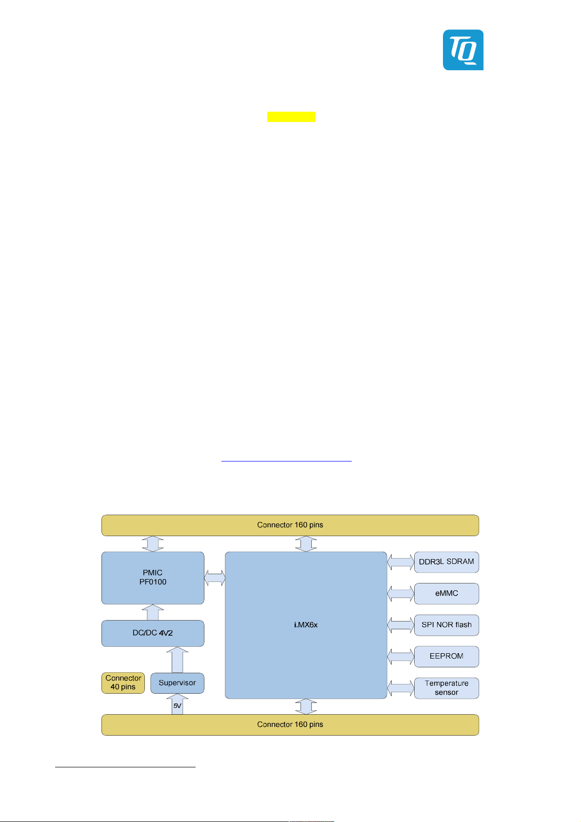
3. ELECTRONICS
The information provided in this User's Manual is only valid in connection with the tailored boot loader,
which is preinstalled on the TQMa6x, and the
3.1 System overview
3.1.1 System architecture / block diagram
BSP provided by TQ-Systems GmbH, see also chapter 5.
Illustration 1: Block diagram TQMa6x
1: It is not possible to boot from an SPI NOR flash bigger than 16 Mbyte.

User's Manual l TQMa6x & TQMa6xP UM 0401 l © 2018, TQ-Systems GmbH Page 5
3.1.2 Functionality
The following key functions are implemented on the TQMa6x:
• i.MX6 CPU
• DDR3L SDRAM
• eMMC NAND flash
• SPI NOR flash
• EEPROM
• Temperature sensor
• Supervisor
• PMIC / DC/DC converter
The following interfaces are provided at the connectors of the TQMa6x: 2
• 1 × Ethernet 10/100/1000 RGMII
• 1 × HDMI 1.4
• 1 × I
2
S
• 1 × JTAG
• 1 × MIPI CSI
• 1 × MIPI DSI
• 1 × MLB
• 1 × Parallel display RGB 24 bit
• 1 × PCIe 2.0 (1 Lane)
• 1 × SATA 3.0
• 1 × SD 8 Bit (SDIO / MMC / SD card)
• 1 × S/PDIF
• 2 × CAN
• 2 × General Purpose Clocks
• 2 × I
2
C
• 2 × LVDS display
• 2 × SPI
• 2 × USB 2.0 Hi-Speed (1 × USB Host, 1 × USB-OTG)
• 40 × GPIO
• 4 × PWM
• 4 × UART (with Handshake)
Further interfaces of the i.MX6 are also available as an alternative to the mentioned factory configuration, by adapting the pin
configuration. These are amongst other:
• Camera Sensor Interfaces
• EIM bus
• Enhanced Periodic Interrupt Timer EPIT
• Enhanced Serial Audio Interface ESAI
• Ethernet 10/100 RMII
• General Purpose Media Interface GPMI
• General Purpose Timer GPT
• Keypad port
• MIPI HSI Host Controller
• More audio interfaces
• More I
2
C interfaces
• More SPI interfaces
• More UARTs
• One additional parallel display
2: Quantity of interfaces depends on the i.MX6 derivative.

User's Manual l TQMa6x & TQMa6xP UM 0401 l © 2018, TQ-Systems GmbH Page 6
3.2 System components
3.2.1 i.MX6
The following block diagram shows the main features of the i.MX6 processor family.
Illustration 2: Block diagram i.MX6
(Source:
NXP)
3.2.1.1 i.MX6 derivatives
Depending on the TQMa6x derivative, one of the following i.MX6 derivatives is assembled:
Table 2: Processor derivatives
Description Clock Temperature range TQ-BSP
i.MX6S Solo Industrial 800 MHz –40 °C to +105 °C Yes
i.MX6U DualLite Industrial 800 MHz –40 °C to +105 °C Yes
i.MX6D Dual Industrial 800 MHz –40 °C to +105 °C Yes
i.MX6Q Quad Industrial 800 MHz –40 °C to +105 °C Yes
i.MX6DP DualPlus Industrial 800 MHz –40 °C to +105 °C Yes
i.MX6QP QuadPlus Industrial 800 MHz –40 °C to +105 °C Yes
3.2.1.2 eFUSEs
The eFUSEs in the i.MX6 are available for the user, except for the MAC address eFUSEs.
TQMa6x modules are delivered pre-programmed with MAC addresses from the TQ-Systems MAC address pool.
The MAC addresses are burned in the designated OCOTP eFUSEs (bank 4, word 2, 3).
The MAC address LOCK-FUSE WP (Write Protect) is burnt, which permits to temporarily overwrite the MAC address for test
purposes. If this is not desired, the MAC address LOCK-FUSE OP (Overwrite Protect) can be burned by the user.
3.2.1.3 i.MX6 errata
Attention: Malfunction
Please take note of the current i.MX6 errata (7), (8).
User's Manual l TQMa6x & TQMa6xP UM 0401 l © 2018, TQ-Systems GmbH Page 7
3.2.1.4 Boot modes
The i.MX6 contains a ROM with integrated boot loader.
After power-up, the boot code initializes the hardware and then loads the program image from the selected boot device.
The eMMC or the SPI NOR flash integrated on the TQMa6x can for example be selected as the standard boot device.
More boot interfaces are available as an alternative to booting from the integrated eMMC or the SPI NOR flash, see 3.2.1.6.
More information about boot interfaces and its configuration is to be taken from the i.MX6 data sheets (1), (2), and (3) as well as
the i.MX6 Reference Manuals (4), (5), and (6).
The boot device and its configuration, as well as different i.MX6 settings have to be set via different boot mode registers.
Therefore, the i.MX6 provides two possibilities:
• Burning internal eFuses
• Reading dedicated GPIO pins
The exact behaviour during booting depends on the value of the register BT_FUSE_SEL.
The following table shows the behaviour of the bit BT_FUSE_SEL in dependence of the selected boot mode.
Table 3: Boot modes and BT_FUSE_SEL
BOOT_MODE[1:0] Boot type
00 (default) Boot from eFuses
01 Serial Downloader n/a
10 Internal Boot
BT_FUSE_SEL = 0: Boot using Serial Loader (default)
BT_FUSE_SEL = 1: Boot configuration is taken from eFuses
BT_FUSE_SEL = 0: Boot configuration is taken from BOOT_CFG pins (default)
BT_FUSE_SEL = 1: Boot configuration is taken from eFuses
BT_FUSE_SEL
Usage
Series production
Development
/ production
Development
11 Reserved n/a n/a
Attention: Malfunction
Burning an eFuse is irreversible!
TQ-Systems GmbH takes no responsibility for the correct operation of the TQMa6x,
if the user burns eFuses.
Attention: Boot configuration
It is recommended to implement a redundant update concept for field software updates
during the carrier board design.
User's Manual l TQMa6x & TQMa6xP UM 0401 l © 2018, TQ-Systems GmbH Page 8
3.2.1.5 Boot configuration
Note: Boot configuration
No boot device is preset when the TQMa6x is delivered.
Some general settings are done with some eFuses independent from the boot device.
Table 4: General boot settings
i.MX6 TQMa6x
eFuse Option Setting 3 Signal Pin
BOOT_CFG1[7:0]
BOOT_CFG2[7:0]
BOOT_CFG3[7]
BOOT_CFG3[6]
BOOT_CFG3[5] 0 BOOT_CFG3_5 X2-99
BOOT_CFG3[4]
BOOT_CFG3[3] Reserved 0 BOOT_CFG3_3 X2-101
BOOT_CFG3[2]
Boot configuration 1:
Specific to selected boot mode
Boot configuration 2:
Specific to selected boot mode
L1 I-Cache DISABLE:
0 = Enabled
1 = Disabled
BT_MMU_DISABLE:
0 = MMU / L1 D Cache / PL310 enabled
1 = MMU / L1 D Cache / PL310 disabled
DDR Memory Map Config:
00 = Single DDR channel
01 = 2 × 32 Map
10 = 4 KB interleaving
11 = Reserved (Solo / DualLite / Dual / Quad)
11 = Extension Mode (DualPlus / QuadPlus)
(see BOOT_CFG3[1:0])
Boot Frequencies ARM / DDR / AXI:
Solo / DualLite:
0 = 792 / 396 / 264 MHz
1 = 396 / 352 / 176 MHz
Dual / Quad / DualPlus / QuadPlus:
0 = 792 / 528 / 264 MHz
1 = 396 / 352 / 176 MHz
– BOOT_CFG1_7:0 –
– BOOT_CFG2_7:0 –
0 BOOT_CFG3_7 X2-97
0 BOOT_CFG3_6 X2-98
0 BOOT_CFG3_4 X2-100
0 BOOT_CFG3_2 X2-102
BOOT_CFG3[1] 0 BOOT_CFG3_1 X2-103
BOOT_CFG3[0]
BOOT_CFG4[7]
BOOT_CFG4[6:0]
DDR Memory Map Extension Config: 4
00 = Single DDR Channel
01 = Fixed 2 × 32 Map
10 = Reserved
11 = Reserved
Debug loop:
0 = Loop disabled
1 = Loop enabled
Boot configuration 4:
Specific to selected boot mode
0 BOOT_CFG3_0 X2-104
0 BOOT_CFG4_7 X2-85
– BOOT_CFG4_6:0 –
3: Voltage level or condition of eFuse.
4: Reserved for Solo, DualLite, Dual, Quad, or if BOOT_CFG3[5:4] is not 0b11.

User's Manual l TQMa6x & TQMa6xP UM 0401 l © 2018, TQ-Systems GmbH Page 9
3.2.1.6 Boot interfaces
In the next chapters, the configuration of the following boot devices is described:
• eMMC
• SPI NOR flash
5
• SD card
3.2.1.7 Boot device eMMC
Table 5: Boot configuration eMMC at uSDHC3
i.MX6 TQMa6x
eFuse Option Setting 6 Signal Pin
BOOT_CFG1[7] 0 BOOT_CFG1_7 X2-115
BOOT_CFG1[6]
BOOT_CFG1[5]
BOOT_CFG1[4]
BOOT_CFG1[3] 0 BOOT_CFG1_3 X2-119
BOOT_CFG1[2]
BOOT_CFG1[1]
BOOT_CFG2[7] 0 BOOT_CFG2_7 X2-107
BOOT_CFG2[6] 1 BOOT_CFG2_6 X2-108
BOOT_CFG2[5]
BOOT_CFG2[4] 1 BOOT_CFG2_4 X2-110
BOOT_CFG2[3]
BOOT_CFG2[2]
BOOT_CFG2[1]
BOOT_CFG2[0]
Boot Device Selection:
01 = Boot from uSDHC Interfaces
SD / MMC-Selection:
0 = SD / eSD / SDXC
1 = MMC / eMMC
Fast Boot Support:
0 = Regular
1 = Fast Boot
MMC Speed Mode:
0x = High Speed Mode
1x = Normal Speed Mode
eMMC Reset Enable:
0 = eMMC-Reset disabled
1 = eMMC-Reset enabled
eMMC Bus Width:
000 = 1 bit
001 = 4 bit
010 = 8 bit
101 = 4 bit DDR (MMC 4.4)
110 = 8 bit DDR (MMC 4.4)
Port Select:
00 = uSDHC1
01 = uSDHC2
10 = uSDHC3
11 = uSDHC4
DLL Override:
0 = Boot ROM
1 = Apply value per eFuse field MMC_DLL_DLY[6:0]
Boot Acknowledge:
0 = Boot Acknowledge enable
1 = Boot Acknowledge disable
Override Pad Settings:
0 = default values
1 = Use PAD_SETTINGS values
1 BOOT_CFG1_6 X2-116
1 BOOT_CFG1_5 X2-117
0 BOOT_CFG1_4 X2-118
0 BOOT_CFG1_2 X2-120
1 BOOT_CFG1_1 X2-121
0 BOOT_CFG2_5 X2-109
0 BOOT_CFG2_3 X2-111
0 BOOT_CFG2_2 X2-112
0 BOOT_CFG2_1 X2-113
0 BOOT_CFG2_0 X2-114
In addition to the mode listed above the following eMMC modes are supported at port uSDHC3.
Table 6: uSDHC3 eMMC modes
eMMC mode 1 Bit 4 Bit 8 Bit Fast Boot DDR
Normal Speed
High Speed
5: It is not possible to boot from an SPI NOR flash bigger than 16 Mbyte.
6: Voltage level or condition of eFuse.
7: Not yet supported by software.
– 7 – 7
– 7 – 7
User's Manual l TQMa6x & TQMa6xP UM 0401 l © 2018, TQ-Systems GmbH Page 10
3.2.1.8 Boot device SPI NOR flash
Table 7: Boot configuration SPI NOR flash at eCSPI1
i.MX6 TQMa6x
eFuse Option Setting 8 Signal Pin
BOOT_CFG1[7] 0 BOOT_CFG1_7 X2-115
BOOT_CFG1[6] 0 BOOT_CFG1_6 X2-116
Boot Device Selection:
0011 = Boot from Serial ROM
BOOT_CFG1[5] 1 BOOT_CFG1_5 X2-117
BOOT_CFG1[4]
BOOT_CFG4[6]
BOOT_CFG4[5] 0 BOOT_CFG4_5 X2-89
BOOT_CFG4[4]
BOOT_CFG4[3]
BOOT_CFG4[2] 0 BOOT_CFG4_2 X2-92
BOOT_CFG4[1] 0 BOOT_CFG4_1 X2-93
BOOT_CFG4[0]
EEPROM Recovery: 9
0 = disabled
1 = enabled
CS select (SPI only):
00 = CS#0
01 = CS#1
10 = CS#2
11 = CS#3
SPI Addressing (SPI only)
0 = 2-bytes (16-bit) (3.75 MHz Clock)
1 = 3 Bytes (24-bit) (15 MHz Clock)
Port Select:
000 = ECSPI-1
001 = ECSPI-2
010 = ECSPI-3
001 = ECSPI-4
100 = ECSPI-5
101 = I2C-1
110 = I2C-2
111 = I2C-3
1 BOOT_CFG1_4 X2-118
0 BOOT_CFG4_6 X2-86
1 BOOT_CFG4_4 X2-90
1 BOOT_CFG4_3 X2-91
0 BOOT_CFG4_0 X2-96
Note: SPI NOR flash size
It is not possible to boot from an SPI NOR flash bigger than 16 Mbyte.
8: Voltage level or condition of eFuse.
9: The i.MX6 supports recovery devices. If this bit is set, the SPI NOR flash serves as recovery boot device.
User's Manual l TQMa6x & TQMa6xP UM 0401 l © 2018, TQ-Systems GmbH Page 11
3.2.1.9 Boot device SD card
Table 8: Boot configuration SD card at uSDHC2
i.MX6 TQMa6x
eFuse Option Setting 10 Signal Pin
BOOT_CFG1[7] 0 BOOT_CFG1_7 X2-115
BOOT_CFG1[6]
BOOT_CFG1[5]
BOOT_CFG1[4]
BOOT_CFG1[3] 0 BOOT_CFG1_3 X2-119
BOOT_CFG1[2]
BOOT_CFG1[1]
BOOT_CFG1[0]
BOOT_CFG2[7] 0 BOOT_CFG2_7 X2-107
BOOT_CFG2[6]
BOOT_CFG2[5]
BOOT_CFG2[4] 0 BOOT_CFG2_4 X2-110
BOOT_CFG2[3]
BOOT_CFG2[1]
BOOT_CFG2[0]
Boot Device Selection:
01 = Boot from uSDHC Interfaces
SD / MMC-Selection:
0 = SD / eSD / SDXC
1 = MMC / eMMC
Fast Boot:
0 = Regular
1 = Fast Boot
SD Speed Mode:
00 = Normal / SDR12
01 = High / SDR25
10 = SDR50 (on uSDHC3 and uSDHC4 only)
11 = SDR104 (on uSDHC3 and uSDHC4 only)
SD Power Cycle Enable:
0 = No Power Cycle
1 = Power cycle enabled via SD_RST pad (on uSDHC3 and uSDHC4 only)
SD Loopback Clock Source Sel (for SDR50 and SDR104 only)
0 = through SD pad
1 = direct
SD Calibration Step:
00 = 1 delay cell
01 = 1 delay cell
10 = 2 delay cell
11 = 3 delay cell
Bus Width:
0 = 1 bit
1 = 4 bit
Port:
00 = uSDHC1
01 = uSDHC2
10 = uSDHC3
11 = uSDHC4
Pull-Down during SD Power Cycle:
0 = Use default SD pad settings during power cycle
1 = Set pull-down on SD pads during power cycle
(only used if "SD Power Cycle Enable" enabled)
Override Pad Settings:
0 = Use default values
1 = Use PAD_SETTINGS values
1 BOOT_CFG1_6 X2-116
0 BOOT_CFG1_5 X2-117
1 BOOT_CFG1_4 X2-118
0 BOOT_CFG1_2 X2-120
0 BOOT_CFG1_1 X2-121
0 BOOT_CFG1_0 X2-122
0 BOOT_CFG2_6 X2-108
1 BOOT_CFG2_5 X2-109
1 BOOT_CFG2_3 X2-111
0 BOOT_CFG2_1 X2-113
0 BOOT_CFG2_0 X2-114
In addition to the mode listed above the following SD card modes are supported at port uSDHC2:
Table 9: uSDHC2 SD card modes
SD mode 1 Bit 4 Bit Fast Boot
SDR12
SDR25
SDR50 – – –
SDR104 – – –
10: Voltage level or condition of eFuse.
User's Manual l TQMa6x & TQMa6xP UM 0401 l © 2018, TQ-Systems GmbH Page 12
3.2.2 Memory
3.2.2.1 DDR3L SDRAM
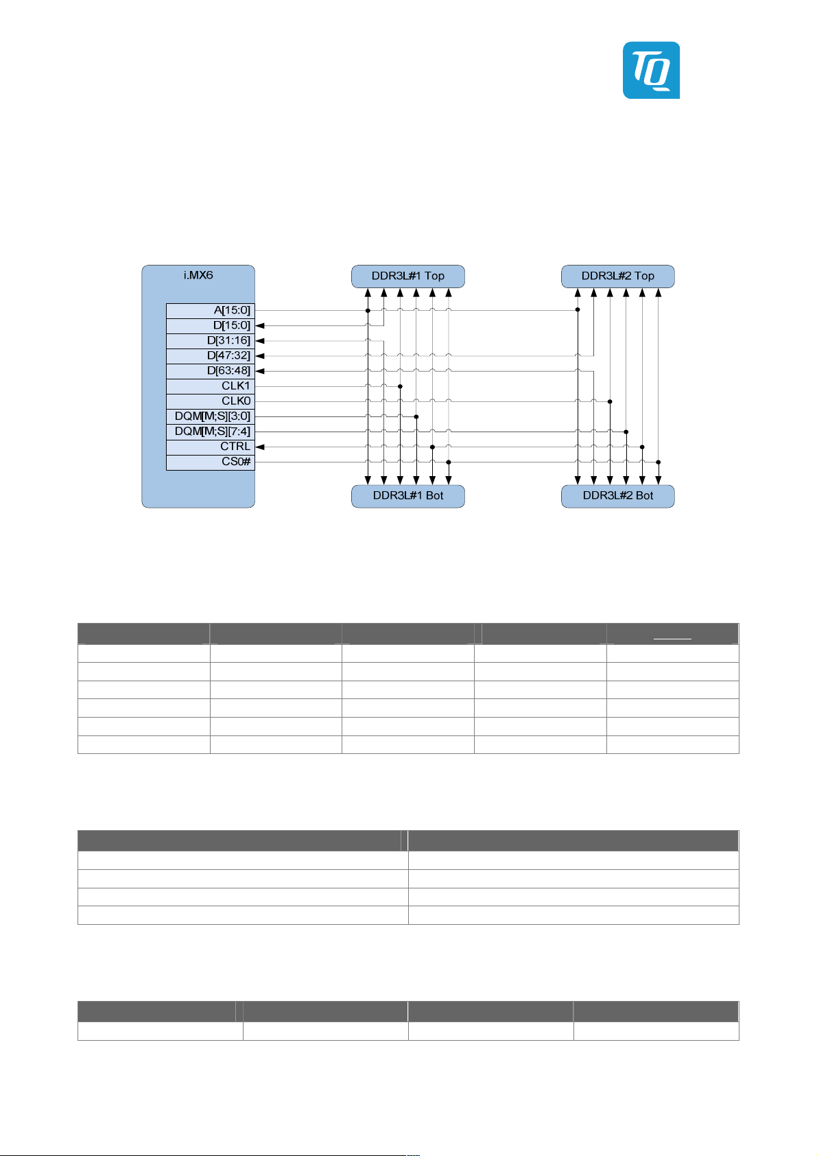
Depending on the i.MX6 derivative either two or four DDR3L SDRAM chips are assembled on the TQMa6x.
All chips have one common chip select. The chips are connected to the i.MX6 with a 64-bit bus.
(Exception: The i.MX6 “Solo” is connected with a 32-bit bus.)
The following block diagram shows how the DDR3L SDRAM is connected to the i.MX6.
Illustration 3: Block diagram DDR3L SDRAM connection
The characteristics of the memory interface depend on the i.MX6 derivative.
The following table shows the different possibilities.
Table 10: i.MX6 SDRAM interface according to i.MX6 derivative
i.MX6 derivative Bus width Clock SDRAM chips TQ-BSP
i.MX6 Solo × 32 396 MHz 2 Yes
i.MX6 DualLite × 64 396 MHz 4 Yes
i.MX6 Dual × 64 528 MHz 4 Yes
i.MX6 DualPlus × 64 528 MHz 4 Yes
i.MX6 Quad × 64 528 MHz 4 Yes
i.MX6 QuadPlus × 64 528 MHz 4 Yes
The assembly options of DDR3L SDRAM on the TQMa6x are listed in the following table.
Table 11: DDR3L SDRAM memory size options
Assembly option Size
2 × DDR3L 128M16 / ×32 512 Mbyte
2 × DDR3L 256M16 / ×32 1 Gbyte
4 × DDR3L 128M16 / ×64 1 Gbyte
4 × DDR3L 256M16 / ×64 2 Gbyte
The following address range is reserved for the DDR controller in mode X32 / X64 fixed:
Table 12: DDR3L SDRAM address range
Start address Size Chip Select Remark
0x1000_0000 0xFFFF_FFFF
CS0# 3840 Mbyte

User's Manual l TQMa6x & TQMa6xP UM 0401 l © 2018, TQ-Systems GmbH Page 13
3.2.2.2 eMMC NAND flash
Attention: Malfunction or destruction
Some Micron eMMC have a too high drive-strength. This can lead to poor signal integrity and a life time
reduction of the i.MX6. When using an own bootloader or operating system it is essential to implement
the SET_DSR routine, which is part of the BSP as of revision 0102.
The SET_DSR routine as of BSP revision 0102 must not
be implemented for TQMa6x as of revision 04xx!
An eMMC NAND flash for the boot loader and the application software is assembled. The Hardware Reset function depends on
the BSP implementation. The following block diagram shows how the eMMC flash is connected to the i.MX6.
i.MX6 eMMC
SD3_CLK
SD3_CMD
SD3_DATA[7:0] DAT[7:0]
CLK
CMD
RESET#SD3_RESET
Illustration 4: Block diagram eMMC NAND flash connection
3.2.2.3 SPI NOR flash
An SPI NOR flash is also available. It can e.g., serve as boot device or as recovery device.
The following block diagram shows how the SPI NOR flash is connected to the i.MX6.
Illustration 5: Block diagram SPI NOR flash connection
The write protection pin of the SPI NOR flash is available at connector X3-40.
The reset pin is not connected by default. A reset can only be carried out via a complete power cycle of the TQMa6x.
The SPI NOR flash can be reset by one or more of the following sources (assembly option).
• WDOG1# (see 3.2.5.25)
• MX6_POR# (see 3.2.6)
• GPIO2_IO01 (see 3.2.5.7)
The SPI NOR flashes, which can be assembled on the TQMa6x, are listed in the following table.
Table 13: SPI NOR flash assembly options
Manufacturer Size Temperature range
Micron 16 Mbyte 11 –40 °C to +85 °C
Micron 32 Mbyte 12 –40 °C to +85 °C
Micron 64 Mbyte 12 –40 °C to +85 °C
Micron 128 Mbyte 12 –40 °C to +85 °C
Attention: Malfunction in SPI-mode
During the boot process, the i.MX6 only supports the 3-byte mode.
Special hardware mechanisms are required for 4-byte mode operation
else erroneous reboots might occur.
11: Maximum size of SPI NOR flash to boot from.
12: Qualification pending.

User's Manual l TQMa6x & TQMa6xP UM 0401 l © 2018, TQ-Systems GmbH Page 14
3.2.2.4 EEPROM
A serial EEPROM is available for permanent storage of e.g. TQMa6x characteristics or customers parameters.
Depending on the TQMa6x version, the I2C1 or the I2C3 bus of the i.MX6 controls the EEPROM, see also 3.2.5.9.
Write-Protection (WP) is not supported.
The following block diagram shows how the EEPROM is connected to the i.MX6.
Illustration 6: Block diagram EEPROM interface
The following table shows the EEPROM used.
Table 14: EEPROM, component
Manufacturer Part number Size Temperature range
STM M24C64-WDW6TP 64 kbit –45 °C to +85 °C
The I2C address of the EEPROM is 0x50 / 101 0000b
In the EEPROM, TQMa6x-specific data is stored. It is, however, not essential for the correct operation of the TQMa6x.
The user can delete or alter the data.
In the following table, the parameters stored in the EEPROM are shown.
Table 15: EEPROM, TQMa6x-specific data
Offset Payload (byte) Padding (byte) Size (byte) Type Remark
0x00
0x20
0x30
0x40
0x80
Variable Variable 32
6
10
(10)
8
8
(10)
16
(10)
16
(10)
Variable Variable 64
– – 8064
Binary Hard Reset Configuration Word (HRCW), (optional)
(10)
Binary MAC address
(10)
ASCII Serial number
(10)
ASCII Order code
(10)
– (Unused)
(10)
User's Manual l TQMa6x & TQMa6xP UM 0401 l © 2018, TQ-Systems GmbH Page 15
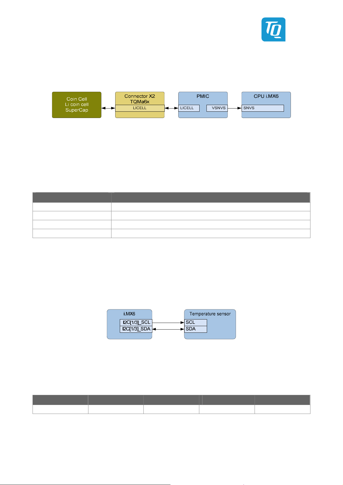
3.2.3 RTC
The i.MX6 provides an RTC, which has its own power domain (SNVS). The accuracy of the RTC is mainly determined by the
characteristics of the quartz used. The type FC-135 used on the TQMa6x has a standard frequency tolerance of
±20 ppm @ +25 °C. The following block diagram shows the implementation on the TQMa6x.
Illustration 7: Block diagram RTC
The RTC power domain SNVS of the i.MX6 is supplied by the PMIC-internal regulator VSNVS. This regulator is supplied either by
VIN (VDD4V2) or by LICELL. LICELL supports coin cells as well as Lithium coin cells or SuperCaps, which can also be charged by
the PMIC. Charging methods and electrical characteristics of the pin LICELL are to be taken from the PMIC data sheet (10).
A coin cell is not suitable for long term bridging because of the high current consumption. A Lithium coin cell or a SuperCap
might be an option depending on the use case. It is to be taken note of that the typical charging current is only 60 µA.
For long term bridging an external RTC connected at the I2C bus on the carrier board is recommended.
Table 16: Current consumption RTC at pin LICELL
Coin Cell voltage PMIC PF0100A, typical current consumption
2.4 V 85 µA
2.7 V 100 µA
3.0 V 115 µA
3.3 V 130 µA
3.2.4 Temperature sensor
A temperature sensor LM75ADP is assembled on the TQMa6x to monitor the temperature of the TQMa6x.
The LM75ADP is placed on the bottom side of the TQMa6x, (D2 in Illustration 22). Depending on the TQMa6x version,
the temperature sensor is connected to the I2C1 or the I2C3 bus of the i.MX6, see also 3.2.5.9.
The following block diagram shows how the temperature sensor is connected to the i.MX6.
Illustration 8: Block diagram temperature sensor interface
The “OS”-output (over-temperature shutdown) of the sensor is not connected.
The following table shows the temperature sensor used.
Table 17: Temperature sensor
Manufacturer Part number Resolution Error Temperature range
NXP LM75ADP 11 bit ADC Max. ±3 °C –55 °C to +125 °C
The I2C address of the temperature sensor is 0x48 / 100 1000b

User's Manual l TQMa6x & TQMa6xP UM 0401 l © 2018, TQ-Systems GmbH Page 16
3.2.5 Interfaces
3.2.5.1 Overview
The TQMa6x provides interfaces with primary functions. They can all be used simultaneously independent of their configuration.
Some of the primary functions cannot be used if a secondary function (e.g. the EIM bus) is used.
Table 18: Internally used interfaces
Interface Number Function Chapter Remark
MMDC 1 Primary 3.2.2.1 Multi-Mode DDR controller
uSDHC3 1 Primary 3.2.2.2 eMMC, 8 bit
ECSPI 1 Primary 3.2.2.3 ECSPI1 / SPI NOR flash
Table 19: Externally available interfaces
Interface Number Function Chapter Remark
AUDMUX
CCM 2 Primary 3.2.5.3 General Purpose Clocks
ECSPI
EIM 1 Secondary – Multiplexing has to be adapted
ENET
EPIT 2 Secondary – EPIT1 / EPIT2 | Multiplexing has to be adapted
ESAI 1 Secondary – Multiplexing has to be adapted
FLEXCAN 2 Primary 3.2.5.6 FLEXCAN1 / FLEXCAN2
GPIO 40 Primary 3.2.5.7 –
GPMI 1 Secondary – Multiplexing has to be adapted
GPT 1 Secondary – Multiplexing has to be adapted
HDMI 1 Primary 3.2.5.8 –
I2C
IPU
KPP 1 Secondary – Multiplexing has to be adapted
LDB 2 Primary 3.2.5.12 LVDS0 / LVDS1
MIPI_CSI 1 Primary 3.2.5.13 –
MIPI_DSI 1 Primary 3.2.5.14 –
MIPI_HSI 1 Secondary – Multiplexing has to be adapted
MLB 1 Primary 3.2.5.15 –
PCIe 1 Primary 3.2.5.16 –
PWM
SATA 1 Primary 3.2.5.18 –
SJC 1 Primary 3.2.5.19 JTAG
S/PDIF 1 Primary 3.2.5.20 –
TAMPER 1 Primary 3.2.5.21 –
UART
USB 2 Primary 3.2.5.23 USB_H1 / USB_OTG
uSDHC
WDOG
XTAL 2 Primary 3.2.5.26 XTALOSC1 / XTALOSC2
1 Primary 3.2.5.2 AUD3 / I2S
3 Secondary – AUD4 / AUD5 / AUD6 | Multiplexing has to be adapted
2 Primary 3.2.5.4 ECSPI1 / ECSPI5
3 Secondary – ECSPI2 / ECSPI3 / ECSPI4 | Multiplexing has to be adapted
1 Primary 3.2.5.5 RGMII (GbE)
1 Secondary – ENET (10/100) / 1588 | Multiplexing has to be adapted
2 Primary 3.2.5.9 I2C1 / I2C3
1 Secondary – I2C2 | Multiplexing has to be adapted
1 Primary 3.2.5.11 DISP0 (RGB)
4 Secondary – CSI0 / CSI1 / DISP0 / DISP1 | Multiplexing has to be adapted
4 Primary 3.2.5.17 PWM1 / PWM3 / PWM4
1 Secondary – PWM2 | Multiplexing has to be adapted
4 Primary 3.2.5.22 UART2 / UART3 / UART4 / UART5
1 Secondary – UART1 | Multiplexing has to be adapted
1 Primary 3.2.5.24 uSDHC2 / SD card / 1/4/8 Bit
2 Secondary – uSDHC1 / uSDHC4 | Multiplexing has to be adapted
1 Primary 3.2.5.25 WDOG1
1 Secondary – WDOG2 | Multiplexing has to be adapted
In the following chapters, only the external primary interfaces are described.

User's Manual l TQMa6x & TQMa6xP UM 0401 l © 2018, TQ-Systems GmbH Page 17
3.2.5.2 AUDMUX
The signals of the digital audio multiplexer 3 (AUD3) are available via SSI on the connectors.
The following table shows the signals used by the AUD3 interface.
Table 20: Signals AUD3
Signal name Direction Signal I2S i.MX6 ball TQMa6x
AUD3_RXC I – M1 X1–99
AUD3_RXD I I2S_DOUT N3 X1–103
AUD3_RXFS I – M3 X1–101
AUD3_TXC O I2S_SCLK N1 X1–100
AUD3_TXD O I2S_DIN P2 X1–104
AUD3_TXFS O I2S_LRCLK N4 X1–102
Signal CCM_CLKO1 is used as I2C_MCLK in the
BSP provided by TQ-Systems GmbH.
Besides I2S, the SSI interface supports more synchronous modes.
Details are to be taken from the NXP Reference Manuals (4), (5), and (6).
3.2.5.3 CCM
The i.MX6 clock controller CCM provides two programmable clocks. The following table shows the signals of the CCM.
Table 21: Signals CCM
Signal name Direction i.MX6 ball TQMa6x Remark
CCM_CLKO1 O P4 X1–78 TQ-BSP: I2S_MCLK
CCM_CLKO2 O A17 X2–82 –
3.2.5.4 ECSPI
The i.MX6 provides five ECSPI interfaces. Primarily ECSPI1 and ECSPI5 are available at the connectors. The i.MX6 derivatives “Solo”
and “DualLite” do not provide ECSPI5. The following table shows the signals used by the ECSPI1 and ECSPI5 interfaces.
Table 22: Signals ECSPI1, ECSPI5
Signal name Direction i.MX6 ball TQMa6x Remark
ECSPI1_SCLK O C25 X2–64 –
ECSPI1_MOSI O D24 X2–66 –
ECSPI1_MISO I F21 X2–63 –
ECSPI1_SS1# O G21 X2–65 Used by optional SPI NOR flash on TQMa6x
ECSPI1_SS2# O F22 X2–72 –
ECSPI1_SS3# O G22 X2–71 –
ECSPI5_SCLK O D20 X1–114 –
ECSPI5_MOSI O B21 X1–110 –
ECSPI5_MISO I A21 X1–108 –
ECSPI5_SS0# O C20 X1–112 –

User's Manual l TQMa6x & TQMa6xP UM 0401 l © 2018, TQ-Systems GmbH Page 18
3.2.5.5 ENET
The i.MX6 provides a 10/100/1000 MAC core, which supports MII, RMII and RGMII.
The RGMII signals are available as primary function at the connectors.
The following table shows the signals used by the RGMII interface.
Table 23: Signals RGMII
Signal name Direction i.MX6 ball TQMa6x Power group
ENET_MDC O V20 X2–49
ENET_MDIO I/O V23 X2–51
NVCC_ENET (2.5 V / 3.3 V)
ENET_REFCLK I V22 X2–50
RGMII_RD3 I D23 X2–43
RGMII_RD2 I B24 X2–41
RGMII_RD1 I B23 X2–39
RGMII_RD0 I C24 X2–37
RGMII_RX_CTL I D22 X2–45
RGMII_RXC I B25 X2–33
RGMII_TD3 O A24 X2–44
NVCC_RGMII (2.5 V)
RGMII_TD2 O E21 X2–42
RGMII_TD1 O F20 X2–40
RGMII_TD0 O C22 X2–38
RGMII_TX_CTL O C23 X2–46
RGMII_TXC O D21 X2–34
Note: NVCC_ENET
NVCC_ENET_IN has to be connected externally!
The RGMII interface of the i.MX6 works with an I/O voltage of 2.5 V. In order to use the interface, additional signals of the signal
group ENET are required. The accompanying power supply pin is routed to the connector to operate these signals on the same
I/O voltage, if RGMII is used.
If RGMII is used, NVCC_ENET_IN has to be connected to VCC2V5_RGMII_OUT.
It is important that all ten signals of the signal group ENET are then also set to 2.5 V.
If RGMII is not required, NVCC_ENET_IN has to be connected to VCC3V3_REF_OUT.
By adapting the multiplexing, it is possible to use MII or RMII.
Details are to be taken from the NXP Reference Manuals (4), (5), and (6).

User's Manual l TQMa6x & TQMa6xP UM 0401 l © 2018, TQ-Systems GmbH Page 19
Attention: Max. load on VCC2V5_RGMII_OUT
In order to spare an additional I/O voltage power supply on the carrier board, the voltage
VCC2V5_RGMII_OUT provided by the TQMa6x can be used as I/O supply voltage for an RGMII-PHY.
VCC2V5_RGMII_OUT provides a maximum of 200 mA, of which the TQMa6x requires approximately
80 mA.
Attention: Special function of TQMa6x pin X1–150
The pad GPIO_16 / ball R2 / signal GPIO7_IO11 of the i.MX6 (TQMa6x pin X1–150) has a special
function with different Ethernet functions. More information is to be taken from the NXP Hardware
Development Guide for i.MX 6Quad, 6Dual, 6DualLite, 6Solo Families of Applications Processors (9).
Note: NXP erratum ERR006687, reduced ENET performance
On account of the NXP erratum ERR006687, which describes reduced ENET performance when
responding to interrupts, new variants were introduced with TQMa6x revision 04xx.
The workaround provided by NXP is implemented on variants “A” and “C” of TQMa6x revision 04xx.
Please note, that the Letters “A”, “B”, and “C” must not be confused with the letters in the order code
of the e.g., TQMa6Q-AA. Please contact
TQ-Support for more information regarding the desired
variant.
The following table shows the three possible variants.
Table 24: ENET-Patch variants
Variant Short description Remark
A 2 × I2C1 + ENET-Patch For Solo, DualLite, Dual, and Quad CPUs, designed to work on MBa6x
B 1 × I2C1 + 1 × I2C3 For DualPlus and QuadPlus, fully backward compatible to TQMa6x revision 01xx
C 1 × I2C1 + ENET-Patch + 1 × GPIO Provides an additional GPIO compared to Variant “A”, not designed to work on MBa6x
Illustration 9, Illustration 10, and Illustration 11 show the different variants, see also 3.2.5.9.

User's Manual l TQMa6x & TQMa6xP UM 0401 l © 2018, TQ-Systems GmbH Page 20
3.2.5.6 FLEXCAN
The i.MX6 provides two integrated CAN controllers. Both pairs of signals are available at the connectors.
The drivers required have to be implemented on the carrier board.
The following table shows the signals used by the CAN interface.
Table 25: Signals FLEXCAN
Signal name Direction i.MX6 ball TQMa6x
CAN1_TX O W6 X1–96
CAN1_RX I W4 X1–94
CAN2_TX O T6 X1–92
CAN2_RX I V5 X1–90
3.2.5.7 GPIO
Beside their interface function, most of the i.MX6 pins can also be used as GPIO.
All these GPIOs can trigger an interrupt. Details are to be taken from the NXP Reference Manuals (4), (5), and (6).
The electrical characteristics of the GPIOs are to be taken from the NXP Data Sheets (1), (2), and (3).
In addition, different pins are already marked as GPIO and are available at the connectors.
The following table shows the GPIO signals used.
Table 26: Signals GPIO
Signal name Direction i.MX6 ball TQMa6x Remark
GPIO1_IO5 I/O R4 X1–86 Only on Variant “C”, see Illustration 11
GPIO1_IO30 I/O U20 X1–149 –
GPIO1_IO29 I/O W20 X1–151 –
GPIO1_IO28 I/O V21 X1–153 –
GPIO1_IO26 I/O W22 X1–154 –
GPIO1_IO25 I/O U21 X1–155 –
GPIO1_IO21 I/O F18 X1–106 –
GPIO1_IO8 I/O R5 X1–157 –
GPIO1_IO7 I/O R3 X1–152 –
GPIO2_IO25 I/O J24 X2–81 –
GPIO2_IO24 I/O J23 X2–83 –
GPIO2_IO23 I/O H24 X2–84 –
GPIO2_IO11 I/O A20 X1–23 –
GPIO2_IO8 I/O D18 X1–21 –
GPIO2_IO3 I/O D17 X1–19 –
GPIO2_IO2 I/O F16 X1–17 –
GPIO2_IO1 I/O C17 X1–15 Optional reset source for SPI NOR flash, see 3.2.2.3
GPIO2_IO0 I/O A18 X1–13 –
GPIO3_IO29 I/O J19 X2–77 –
GPIO3_IO28 I/O G23 X2–78 –
GPIO3_IO27 I/O E25 X2–75 –
GPIO3_IO26 I/O E24 X2–76 –
GPIO3_IO23 I/O D25 X2–69 –
GPIO3_IO20 I/O G20 X2–68 –
GPIO4_IO9 I/O U6 X2–58 –
GPIO4_IO8 I/O U7 X2–57 –
GPIO4_IO7 I/O V6 X2–55 –
GPIO4_IO6 I/O W5 X1–74 –
GPIO4_IO5 I/O P5 X1–113 –
GPIO5_IO21 I/O M2 X1–84 –
GPIO5_IO20 I/O P3 X1–111 –
GPIO5_IO18 I/O P1 X1–82 –
GPIO6_IO31 I/O N22 X2–126 –
GPIO6_IO16 I/O D16 X2–94 –
GPIO6_IO14 I/O C16 X1–31 –
GPIO6_IO11 I/O F15 X1–29 –
GPIO6_IO8 I/O A16 X1–27 –
GPIO6_IO7 I/O C15 X1–25 –
GPIO7_IO13 I/O P6 X1–148 –
GPIO7_IO12 I/O R1 X1–72 –
GPIO7_IO11 I/O R2 X1–150 –

User's Manual l TQMa6x & TQMa6xP UM 0401 l © 2018, TQ-Systems GmbH Page 21
3.2.5.8 HDMI
The i.MX6 provides an integrated HDMIv1.4 controller plus PHY.
The following table shows the signals used by the HDMI interface.
Table 27: Signals HDMI
Signal name Direction i.MX6 ball TQMa6x
HDMI_CLK_P O J6 X1–40
HDMI_CLK_N O J5 X1–38
HDMI_D2_P O K4 X1–58
HDMI_D2_N O K3 X1–56
HDMI_D1_P O J4 X1–52
HDMI_D1_N O J3 X1–50
HDMI_D0_P O K6 X1–46
HDMI_D0_N O K5 X1–44
HDMI_DDC_SCL O U5 X1–62
HDMI_DDC_SDA I/O T7 X1–64
HDMI_HPD I K1 X1–66
3.2.5.9 I
2
C
The i.MX6 derivatives “Solo” and “DualLite” provide four, the i.MX6 derivatives “Dual”, “DualPlus”, “Quad”, and “QuadPlus”
provide three I2C interfaces. I2C1 and I2C3 are available at the connectors as primary function. For details see 3.2.5.10.
The following table shows the signals used by the I2C interfaces.
Table 28: Signals I2C
Signal name Dir. i.MX6 ball TQMa6x Remark
I2C1_SCL O N5 X1–107
I2C1_SDA I/O N6 X1–109
4.7 kΩ PU to 3.3 V on TQMa6x, no PU on Variant “B”, see Illustration 10
4.7 kΩ PU to 3.3 V on TQMa6x, no PU on Variant “B”, see Illustration 10
I2C3_SCL O R4 X1–86 4.7 kΩ PU to 3.3 V on TQMa6x Variant “B”, see Illustration 10
I2C3_SDA I/O T3 X1–88 4.7 kΩ PU to 3.3 V on TQMa6x Variant “B”, see Illustration 10
The following table shows the I2C devices connected either to the I2C1 or the I2C3 bus on the TQMa6x
(depending on the Variant, see Illustration 9, Illustration 10, and Illustration 11).
Table 29: I2C address assignment
Component Address
EEPROM (M24C64)
Temperature sensor (LM75A)
PMIC (PF0100A)
0x50 / 101 0000b
0x48 / 100 1000b
0x08 / 000 1000b
If more devices are connected to the I2C buses on the carrier board, the maximum capacitive bus load according to the I2C
standard has to be taken note of. If necessary, additional Pull-Ups at the bus should be provided on the carrier board.

User's Manual l TQMa6x & TQMa6xP UM 0401 l © 2018, TQ-Systems GmbH Page 22
3.2.5.10 I
2
C / ENET-Patch Variants
For TQMa6x revision 04xx to be backward compatible with TQMa6x revision 02xx, the I2C bus configuration varies on account
of Erratum ERR006687 (see also chapter 3.2.5.5).
Variant “A” is preferred for TQMa6x with “Solo”, “DualLite”, “Dual”, and “Quad” CPUs.
Erratum ERR006687 is fixed in “DualPlus” and “QuadPlus” CPUs.
The following block diagrams show the different Variants.
TQMa6x.04xx Variant “A” is compatible with the Starterkit MBa6x.
Illustration 9: ENET-Patch Variant “A”
TQMa6x.04xx Variant “B” is also fully backward compatible (HW + SW) with designs based on TQMa6x revision 01xx.
Illustration 10: ENET-Patch Variant “B”
TQMa6x.04xx Variant “C” provides an additional GPIO compared to Variant “A” but is not compatible with the MBa6x.
Illustration 11: ENET-Patch Variant “C”

User's Manual l TQMa6x & TQMa6xP UM 0401 l © 2018, TQ-Systems GmbH Page 23
3.2.5.11 IPU
The i.MX6 provides two parallel display interfaces (maximum resolution: 4096 × 2048). One of them, DISP0, is routed to the
connectors as primary function. Information with respect to the supported types of displays and formats are to be taken from the
NXP Reference Manuals (4), (5), and (6).
The following table shows the signals used by the display interface DISP0.
Table 30: Signals parallel display DISP0
Signal name Direction i.MX6 ball TQMa6x Remark
DISP0_DAT23 O W24 X2–158 Display Output RGB-Data i.MX6 signal: IPU1_DISP0_DATA23
DISP0_DAT22 O V24 X2–157 Display Output RGB-Data i.MX6 signal: IPU1_DISP0_DATA22
DISP0_DAT21 O T20 X2–156 Display Output RGB-Data i.MX6 signal: IPU1_DISP0_DATA21
DISP0_DAT20 O U22 X2–155 Display Output RGB-Data i.MX6 signal: IPU1_DISP0_DATA20
DISP0_DAT19 O U23 X2–154 Display Output RGB-Data i.MX6 signal: IPU1_DISP0_DATA19
DISP0_DAT18 O V25 X2–153 Display Output RGB-Data i.MX6 signal: IPU1_DISP0_DATA18
DISP0_DAT17 O U24 X2–152 Display Output RGB-Data i.MX6 signal: IPU1_DISP0_DATA17
DISP0_DAT16 O T21 X2–151 Display Output RGB-Data i.MX6 signal: IPU1_DISP0_DATA16
DISP0_DAT15 O T22 X2–150 Display Output RGB-Data i.MX6 signal: IPU1_DISP0_DATA15
DISP0_DAT14 O U25 X2–149 Display Output RGB-Data i.MX6 signal: IPU1_DISP0_DATA14
DISP0_DAT13 O R20 X2–148 Display Output RGB-Data i.MX6 signal: IPU1_DISP0_DATA13
DISP0_DAT12 O T24 X2–147 Display Output RGB-Data i.MX6 signal: IPU1_DISP0_DATA12
DISP0_DAT11 O T23 X2–144 Display Output RGB-Data i.MX6 signal: IPU1_DISP0_DATA11
DISP0_DAT10 O R21 X2–143 Display Output RGB-Data i.MX6 signal: IPU1_DISP0_DATA10
DISP0_DAT9 O T25 X2–142 Display Output RGB-Data i.MX6 signal: IPU1_DISP0_DATA9
DISP0_DAT8 O R22 X2–141 Display Output RGB-Data i.MX6 signal: IPU1_DISP0_DATA8
DISP0_DAT7 O R24 X2–140 Display Output RGB-Data i.MX6 signal: IPU1_DISP0_DATA7
DISP0_DAT6 O R23 X2–139 Display Output RGB-Data i.MX6 signal: IPU1_DISP0_DATA6
DISP0_DAT5 O R25 X2–138 Display Output RGB-Data i.MX6 signal: IPU1_DISP0_DATA5
DISP0_DAT4 O P20 X2–137 Display Output RGB-Data i.MX6 signal: IPU1_DISP0_DATA4
DISP0_DAT3 O P21 X2–136 Display Output RGB-Data i.MX6 signal: IPU1_DISP0_DATA3
DISP0_DAT2 O P23 X2–135 Display Output RGB-Data i.MX6 signal: IPU1_DISP0_DATA2
DISP0_DAT1 O P22 X2–134 Display Output RGB-Data i.MX6 signal: IPU1_DISP0_DATA1
DISP0_DAT0 O P24 X2–133 Display Output RGB-Data i.MX6 signal: IPU1_DISP0_DATA0
DISP0_HSYNC O N25 X2–128 Display Output Horizontal Sync i.MX6 signal: IPU1_DI0_PIN2
DISP0_VSYNC O N20 X2–130 Display Output Vertical Sync i.MX6 signal: IPU1_DI0_PIN3
DISP0_CLK O N19 X2–125 Display Output Clock i.MX6 signal: IPU1_DI0_DISP_CLK
DISP0_DRDY O N21 X2–127 Display Output Data Enable i.MX6 signal: IPU1_DI0_PIN15
DISP0_CONTRAST O P25 X2–129 Display Backlight PWM i.MX6 signal: IPU1_DI0_PIN4 13
13: Currently not supported; use PWM1 instead.

User's Manual l TQMa6x & TQMa6xP UM 0401 l © 2018, TQ-Systems GmbH Page 24
3.2.5.12 LDB
The i.MX6 provides two integrated LVDS display-bridges, which are routed to the connectors.
The following table shows the signals used by the LVDS0 interface.
Table 31: Signals LVDS0, LVDS1
Signal name Direction i.MX6 ball TQMa6x
LVDS0_CLK_P O V3 X1–138
LVDS0_CLK_N O V4 X1–136
LVDS0_TX3_P O W1 X1–144
LVDS0_TX3_N O W2 X1–142
LVDS0_TX2_P O V1 X1–132
LVDS0_TX2_N O V2 X1–130
LVDS0_TX1_P O U3 X1–126
LVDS0_TX1_N O U4 X1–124
LVDS0_TX0_P O U1 X1–120
LVDS0_TX0_N O U2 X1–118
LVDS1_CLK_P O Y4 X1–137
LVDS1_CLK_N O Y3 X1–135
LVDS1_TX3_P O AA4 X1–143
LVDS1_TX3_N O AA3 X1–141
LVDS1_TX2_P O AB2 X1–131
LVDS1_TX2_N O AB1 X1–129
LVDS1_TX1_P O AA1 X1–125
LVDS1_TX1_N O AA2 X1–123
LVDS1_TX0_P O Y2 X1–119
LVDS1_TX0_N O Y1 X1–117

User's Manual l TQMa6x & TQMa6xP UM 0401 l © 2018, TQ-Systems GmbH Page 25
3.2.5.13 MIPI_CSI
The i.MX6 provides a MIPI Camera Sensor Interface (CSI), which is routed to connector X3.
The following table shows the signals used by the MIPI_CSI interface.
Table 32: Signals MIPI_CSI
Signal name Direction i.MX6 ball TQMa6x
CSI_CLK0_P I F3 X3–5
CSI_CLK0_N I F4 X3–3
CSI_D3_P I F1 X3–29
CSI_D3_N I F2 X3–27
CSI_D2_P I E2 X3–23
CSI_D2_N I E1 X3–21
CSI_D1_P I D2 X3–17
CSI_D1_N I D1 X3–15
CSI_D0_P I E3 X3–11
CSI_D0_N I E4 X3–9
3.2.5.14 MIPI_DSI
The i.MX6 provides a MIPI Display Serial Interface (DSI), which is routed to connector X3.
The following table shows the signals used by the MIPI_DSI interface.
Table 33: Signals MIPI_DSI
Signal name Direction i.MX6 ball TQMa6x
DSI_CLK0_P O H4 X3–24
DSI_CLK0_N O H3 X3–22
DSI_D1_P O H1 X3–36
DSI_D1_N O H2 X3–34
DSI_D0_P O G1 X3–30
DSI_D0_N O G2 X3–28
3.2.5.15 MLB
14
The i.MX6 provides, depending on the derivative, a Media-Local-Bus interface (MLB), which is routed to the connectors.
The following table shows the signals used by the MLB interface.
Table 34: Signals MLB
Signal name Direction i.MX6 ball TQMa6x
MLB_C_P I B11 X3–6
MLB_C_N I A11 X3–4
MLB_S_P I/O B9 X3–18
MLB_S_N I/O A9 X3–16
MLB_D_P I/O A10 X3–12
MLB_D_N I/O B10 X3–10
14: Currently not supported.

User's Manual l TQMa6x & TQMa6xP UM 0401 l © 2018, TQ-Systems GmbH Page 26
3.2.5.16 PCIe
The i.MX6 provides a PCIe interface, which is routed to the connectors.
The following table shows the signals used by the PCIe interface.
Table 35: Signals PCIe
Signal name Direction i.MX6 ball TQMa6x
PCIE_TX_P O B3 X1–16
PCIE_TX_N O A3 X1–14
PCIE_RX_P I B2 X1–22
PCIE_RX_N I B1 X1–20
CLK1 can be used as a differential clock (see 3.2.5.26).
3.2.5.17 PWM
The i.MX6 provides several PWMs, which are routed to the connectors.
The following table shows the available PWM signals.
Table 36: Signals PWM
Signal name Direction i.MX6 ball TQMa6x Remark
PWM1 O T2 X1–147 TQ-BSP: BACKLIGHT_PWM (DISP0_CONTRAST)
PWM3 O B19 X1–33 –
PWM4 O F17 X1–105 –
3.2.5.18 SATA
The i.MX6 provides a SATA controller with integrated PHY.
The following table shows the signals used by the SATA interface.
Table 37: Signals SATA
Signal name Direction i.MX6 ball TQMa6x
SATA_TX_P O A12 X1–63
SATA_TX_N O B12 X1–61
SATA_RX_P I B14 X1–57
SATA_RX_N I A14 X1–55

User's Manual l TQMa6x & TQMa6xP UM 0401 l © 2018, TQ-Systems GmbH Page 27
3.2.5.19 SJC
The i.MX6 can operate in two different JTAG modes. The pin JTAG_MOD defines the mode.
The following table shows the existing modes as well as the mode set on the TQMa6x.
Table 38: JTAG modes
JTAG_MOD Name Remark
0 (default) Daisy Chain All For common SW debug (High speed and series production)
1 SJC only IEEE 1149.1 JTAG compliant mode
The following table shows the signals used by the JTAG interface.
Table 39: Signals JTAG
Signal name Direction i.MX6 ball TQMa6x Remark
JTAG_TCK I H5 X1–77 i.MX6-internal PU 47 kΩ
JTAG_TMS I C3 X1–69 i.MX6-internal PU 47 kΩ
JTAG_TDI I G5 X1–71 i.MX6-internal PU 47 kΩ
JTAG_TDO O G6 X1–73 i.MX6-internal keeper
JTAG_TRST# I C2 X1–67 i.MX6-internal PU 47 kΩ
JTAG_MOD I H6 X1–75 4.7 kΩ PD on TQMa6x + i.MX6-internal 100 kΩ PU
3.2.5.20 S/PDIF
The i.MX6 provides an S/PDIF interface with transmit and receive functionality.
The following table shows the signals used by the S/PDIF interface.
Table 40: Signals S/PDIF
Signal name Direction i.MX6 ball TQMa6x
SPDIF_IN I W23 X1–158
SPDIF_OUT O W21 X1–156
3.2.5.21 Tamper
The i.MX6 provides protection against unauthorised opening or manipulation of a device by tamper detection.
The pin TAMPER is available at the connectors for this purpose.
The following table shows the signal used.
Table 41: Signal TAMPER
Signal name Direction i.MX6 ball TQMa6x
TAMPER I E11 X3–39
Details about the behaviour of the TAMPER pin are to be taken from the NXP Reference Manuals (4), (5), and (6).

User's Manual l TQMa6x & TQMa6xP UM 0401 l © 2018, TQ-Systems GmbH Page 28
3.2.5.22 UART
The i.MX6 provides five UART interfaces. UART2 to UART5 also provide handshake signals.
All four interfaces (UART2 to UART5) are available as primary function at the connectors.
Illustration 12: Block diagram UART interfaces
The following table shows the signals used by the UART interfaces.
Table 42: Signals UARTs
Signal name Direction i.MX6 ball TQMa6x Remark
UART5_TXD O M4 X1–91 –
UART5_RXD I M5 X1–89 –
UART5_CTS# O L6 X1–95 –
UART5_RTS# I M6 X1–93 –
UART4_TXD O M2 X1–83 –
UART4_RXD I L1 X1–81 –
UART4_CTS# O L3 X1–87 –
UART4_RTS# I L4 X1–85 –
UART3_TXD O B17 X2–61 –
UART3_RXD I E16 X2–59 –
UART3_CTS# O J20 X2–80 –
UART3_RTS# I H21 X2–79 –
UART2_TXD O D19 X2–29 –
UART2_RXD I E18 X2–27 –
UART2_CTS# O B20 X2–30 Multiplexed as GPIO in the TQ-BSP
UART2_RTS# I C19 X2–28 Multiplexed as GPIO in the TQ-BSP

User's Manual l TQMa6x & TQMa6xP UM 0401 l © 2018, TQ-Systems GmbH Page 29
3.2.5.23 USB
The TQMa6x provides one USB Host controller and one USB OTG controller. USB HOST1 and USB OTG provide an integrated
High-Speed PHY. USB HOST1 and USB OTG are available at the connectors as primary function.
The following table shows the signals used by the USB_H1 interface.
Table 43: Signals USB_H1
Signal name Direction i.MX6 ball TQMa6x Remark
USB_H1_DP I/O E10 X1–32 –
USB_H1_DN I/O F10 X1–34 –
USB_H1_PWR O T5 X1–39 –
USB_H1_OC I R7 X1–41 High-active
USB_H1_VBUS P D10 X1–37 Should be directly connected to a 5 V supply.
The following table shows the signals used by the USB_OTG interface.
Table 44: Signals USB_OTG
Signal name Direction i.MX6 ball TQMa6x Remark
USB_OTG_DP I/O A6 X1–49 –
USB_OTG_DN I/O B6 X1–51 –
Device Mode: connect to Micro-USB connector
USB_OTG_ID I T4 X1–45
Host Mode: connect to Micro-USB connector and to
Ground
USB_OTG_PWR O E23 X2–70 –
USB_OTG_OC# I H20 X2–67 Low-active
USB_OTG_VBUS P E9 X1–43 –
3.2.5.24 uSDHC
The uSDHC2 port of the i.MX6 is routed to the connectors to connect an MMC, SD or SDIO card.
The following table shows the signals used by the uSDHC interface.
Table 45: Signals uSDHC2
Signal name Direction i.MX6 ball TQMa6x
SD2_DAT7 I/O C18 X2–10
SD2_DAT6 I/O E17 X2–9
SD2_DAT5 I/O B18 X2–8
SD2_DAT4 I/O A19 X2–7
SD2_DAT3 I/O B22 X2–6
SD2_DAT2 I/O A23 X2–5
SD2_DAT1 I/O E20 X2–4
SD2_DAT0 I/O A22 X2–3
SD2_CLK O C21 X2–13
SD2_CMD I/O F19 X2–12
SD2_CD# I R6 X2–14
SD2_WP O T1 X2–11

User's Manual l TQMa6x & TQMa6xP UM 0401 l © 2018, TQ-Systems GmbH Page 30
3.2.5.25 Watchdog
The i.MX6 provides a watchdog timer.
The following table shows the signal used by the watchdog timer.
Table 46: Signal WDOG
Signal name Direction i.MX6 ball TQMa6x
WDOG1# O E19 X2–60
The watchdog of the i.MX6 has two functions:
• Power-down counter
After the i.MX6 is reset, a power-down counter is automatically started. If this is not deactivated within 16 seconds,
signal WDOG1# becomes active. More information is to be taken from the NXP Reference Manuals (4), (5), and (6).
• Watchdog timer
If the watchdog timer is activated and is not reset within the configured time, signal WDOG1# is activated.
At the same time, the i.MX6 System Reset Controller triggers a warm reset.
Signal WDOG1# remains at low level or Hi-Z until the next power-on reset.
More information is to be taken from the NXP Reference Manuals (4), (5), and (6).
Optionally, the watchdog can be used as a reset source for the SPI-NOR flash.
3.2.5.26 XTAL
The i.MX6 provides two differential clock outputs, which are routed to the connectors.
The following table shows the signals used.
Table 47: Signals XTAL
Signal name Direction i.MX6 ball TQMa6x
CLK2_P O D5 X3–35
CLK2_N O C5 X3–33
CLK1_P O D7 X1–28
CLK1_N O C7 X1–26

User's Manual l TQMa6x & TQMa6xP UM 0401 l © 2018, TQ-Systems GmbH Page 31
3.2.6 Reset
A reset input and a reset output is available at the connectors of the TQMa6x.
The following block diagram shows the wiring of the reset signals.
Illustration 13: Block diagram Reset
The following table describes the reset signals available at the connectors.
Table 48: Reset signals
Signal name i.MX6 ball TQMa6x Direction Remark
• Reset input POR_B (Power-On Reset) of the i.MX6
• Triggers an i.MX6 COLD reset
MX6_POR# C12 X2–23 IPU 100 kΩ
• Low-active
• Minimal duration to trigger a reliable Reset: app. 30 µs,
see also (1), (2), and (3)
• PMIC Reset output RESETBMCU
RESET_OUT# – X2–25 OOD
• Can be used to reset external periphery
• Open Drain, requires Pull-Up on the carrier board (max. 3.3 V)

User's Manual l TQMa6x & TQMa6xP UM 0401 l © 2018, TQ-Systems GmbH Page 32
3.2.7 Power supply
3.2.7.1 Overview TQMa6x power supply
The input voltage for the TQMa6x is 5 V ±5 % (4.75 V to 5.25 V).
In addition to the required PMIC, another voltage converter is assembled on the TQMa6x to provide the 4.2 V for the PMIC.
Illustration 14: Block diagram power supply
The characteristics and functions of the single pins and signals are to be taken from the PMIC data sheet (10) or the i.MX6
Reference Manuals (4), (5), and (6). The following block diagram shows the circuitry between PMIC and i.MX6.
Illustration 15: Block diagram PMIC signals
Attention: Malfunction or destruction
Improper PMIC programming may cause the i.MX6 or other components on the TQMa6x
to operate outside their specification.
This can lead to malfunction, deterioration or destruction of the TQMa6x.

User's Manual l TQMa6x & TQMa6xP UM 0401 l © 2018, TQ-Systems GmbH Page 33
3.2.7.2 Voltage monitoring VCC5V
A supervisor on the TQMa6x monitors the input voltage of the TQMa6x (VCC5V). If the input voltage is too low, the input
regulator DCDC4V2 is not enabled or disabled. The supervisor triggers typically at 4.55 V ±100 mV and has a delay of 200 ms.
The following block diagram shows the wiring.
Illustration 16: Block diagram VCC5V monitoring
With signal TQM_PWR_OFF# the TQMa6x can be switched off completely. This ensures the lowest possible power consumption.
If TQM_PWR_OFF# is not used, the pin can remain open or be connected to 5 V (TQMa6x supply).
To switch off the TQMa6x, TQM_PWR_OFF# has to be connected to GND.
Attention: Malfunction or destruction
The voltage monitoring does not detect an exceedance of the maximum permitted input voltage.
A too high input voltage can cause malfunction, deterioration or destruction of the TQMa6x.

User's Manual l TQMa6x & TQMa6xP UM 0401 l © 2018, TQ-Systems GmbH Page 34
3.2.7.3 Power consumption TQMa6x
The given current consumption has to be seen as an approximate value.
The power consumption of the TQMa6x strongly depends on the application, the mode of operation and the operating system.
The following table shows details of the TQMa6x supply and power consumption.
Table 49: Power consumption TQMa6x
TQMa6x Mode of operation Current @ 5 V Power consumption Remark
(All) Power-Off 300 µA ~ 1.5 mW –
U-Boot prompt 146 mA ~ 0.73 W –
TQMa6S
Linux prompt 184 mA ~ 0.92 W –
Linux: 100 % CPU load 380 mA ~ 1.90 W –
Calculated peak 1591 mA ~ 7.96 W Theoretical value
U-Boot prompt – – (Not measured)
TQMa6U
Linux prompt – – (Not measured)
Linux: 100 % CPU load – – (Not measured)
Calculated peak 2251 mA ~ 11.26 W Theoretical value
U-Boot prompt – – (Not measured)
TQMa6D
Linux prompt – – (Not measured)
Linux: 100 % CPU load – – (Not measured)
Calculated peak 2221 mA ~ 11.11 W Theoretical value
U-Boot prompt 205 mA ~ 1.03 W –
TQMa6Q
Linux prompt 245 mA ~ 1.23 W –
Linux: 100 % CPU load 830 mA ~ 4.15 W –
Calculated peak 2489 mA ~ 12.45 W Theoretical value
U-Boot prompt 232 mA ~ 1.16 W –
TQMa6DP
Linux prompt – – (Not measured)
Linux: 100 % CPU load 680 mA ~ 3.40 W –
Calculated peak 2979 mA ~ 14.90 W Theoretical value
U-Boot prompt 232 mA ~ 1.16 W –
TQMa6QP
Linux prompt – – (Not measured)
Linux: 100 % CPU load 830 mA ~ 4.15 W –
Calculated peak 3358 mA ~ 16.79 W Theoretical value

User's Manual l TQMa6x & TQMa6xP UM 0401 l © 2018, TQ-Systems GmbH Page 35
3.2.7.4 Power-Up sequence TQMa6x / carrier board
The TQMa6x operates with 5 V; the 3.3 V I/O voltages of the i.MX6 signals are generated on the TQMa6x.
This leads to requirements for the carrier board design concerning the chronological characteristics of the voltages generated on
the carrier board.
Note: Power-Up sequence on the carrier board
To ensure a correct Power-Up, the following sequence must be met on the carrier board:
The supply voltage of 5 V for the TQMa6x is present and the carrier board supply of 3.3 V
is activated by TQMa6x pin VCC3V3MB_EN (X2–26).
The following block diagram shows how VCC3V3MB_EN controls the voltage regulator on a carrier board.
Illustration 17: Block diagram power supply carrier board
No modifications need to be made to carrier boards developed for TQMa6x revision 01xx using pin VCC3V3_REF_OUT (X2-56)
to activate the 3.3 V controller.
For re-designs or new designs, however, signal VCC3V3MB_EN (X2-26), available as of TQMa6x revision 02xx, is recommended.
Attention: Power-Up sequence
To avoid cross-supply and errors in the power-up sequence, no I/O pins may be driven by external
components until the power-up sequence has been completed.
The end of the power-up sequence is indicated by a high level of signal VCC3V3MB_EN.
3.3 TQMa6x interface
3.3.1 Pin multiplexing
When using the i.MX6 signals, the multiple pin configurations by different i.MX6-internal function units must be taken note of.
The pin assignment listed in Table 50, Table 51 and Table 52 refer to the corresponding BSP provided by TQ-Systems GmbH
in combination with the Starterkit MBa6x. The electrical and pin characteristics are to be taken from the i.MX6 and PMIC
documentation (1), (2), (3), (4), (5), (6), and (10).
Attention: Malfunction or destruction
Depending on the configuration, many of the i.MX6 pins can provide several different functions.
Please take note of the information in the i.MX6 Reference Manuals (4), (5), and (6), concerning the
configuration of these pins before integration or start-up of your carrier board / Starterkit.
Improper programming by operating software can cause malfunctions, deterioration or destruction
of the TQMa6x.

User's Manual l TQMa6x & TQMa6xP UM 0401 l © 2018, TQ-Systems GmbH Page 36
3.3.2 Pinout connector X1
Table 50: Pinout connector X1
Ball I/O Level Group Signal Pin Signal Group Level I/O Ball
– P 5 V POWER VCC5V 1 2 VCC5V POWER 5 V P –
– P 5 V POWER VCC5V 3 4 VCC5V POWER 5 V P –
– P 5 V POWER VCC5V 5 6 VCC5V POWER 5 V P –
– P 0 V POWER DGND 7 8 DGND POWER 0 V P –
– P 0 V POWER DGND 9 10 DGND POWER 0 V P –
– P 0 V POWER DGND 11 12 DGND POWER 0 V P –
A18 I/O 3.3 V GPIO GPIO2_IO00 13 14 PCIE_TX_N PCIE – 15 O A3
C17 I/O 3.3 V GPIO GPIO2_IO01 15 16 PCIE_TX_P PCIE – 15 O B3
F16 I/O 3.3 V GPIO GPIO2_IO02 17 18 DGND POWER 0 V P –
D17 I/O 3.3 V GPIO GPIO2_IO03 19 20 PCIE_RX_N PCIE – 15 I B1
D18 I/O 3.3 V GPIO GPIO2_IO08 21 22 PCIE_RX_P PCIE – 15 I B2
A20 I/O 3.3 V GPIO GPIO2_IO11 23 24 DGND POWER 0 V P –
C15 I/O 3.3 V GPIO GPIO6_IO07 25 26 CLK1_N XTAL 2.5 V O C7
A16 I/O 3.3 V GPIO GPIO6_IO08 27 28 CLK1_P XTAL 2.5 V O D7
F15 I/O 3.3 V GPIO GPIO6_IO11 29 30 DGND POWER 0 V P –
C16 I/O 3.3 V GPIO GPIO6_IO14 31 32 USB_H1_DP USB – 16 I/O E10
B19 O 3.3 V PWM PWM3 33 34 USB_H1_DN USB – 16 I/O F10
– P 0 V POWER DGND 35 36 DGND POWER 0 V P –
D10 P 5 V POWER USB_H1_VBUS 37 38 HDMI_CLK_N HDMI – 17 O J5
T5 O 3.3 V USB USB_H1_PWR 39 40 HDMI_CLK_P HDMI – 17 O J6
R7 I 3.3 V USB USB_H1_OC 41 42 DGND POWER 0 V P –
E9 P 5 V POWER USB_OTG_VBUS 43 44 HDMI_D0_N HDMI – 17 O K5
T4 I 3.3 V USB USB_OTG_ID 45 46 HDMI_D0_P HDMI – 17 O K6
– P 0 V POWER DGND 47 48 DGND POWER 0 V P –
A6 I/O – 16 USB USB_OTG_DP 49 50 HDMI_D1_N HDMI – 17 O J3
B6 I/O – 16 USB USB_OTG_DN 51 52 HDMI_D1_P HDMI – 17 O J4
– P 0 V POWER DGND 53 54 DGND POWER 0 V P –
A14 I – 18 SATA SATA_RX_N 55 56 HDMI_D2_N HDMI – 17 O K3
B14 I – 18 SATA SATA_RX_P 57 58 HDMI_D2_P HDMI – 17 O K4
– P 0 V POWER DGND 59 60 DGND POWER 0 V P –
B12 O – 18 SATA SATA_TX_N 61 62 HDMI_DDC_SCL HDMI – 17 O U5
A12 O – 18 SATA SATA_TX_P 63 64 HDMI_DDC_SDA HDMI – 17 I/O T7
– P 0 V POWER DGND 65 66 HDMI_HPD HDMI – 17 I K1
C2 I 3.3 V JTAG JTAG_TRST# 67 68 BOOT_MODE0 CONFIG 3.0 V 19 I
C3 I 3.3 V JTAG JTAG_TMS 69 70 BOOT_MODE1 CONFIG 3.0 V 19 I
C12
iPD
F12
iPD
G5 I 3.3 V JTAG JTAG_TDI 71 72 GPIO7_IO12 GPIO 3.3 V I/O R1
G6 O 3.3 V JTAG JTAG_TDO 73 74 GPIO4_IO06 GPIO 3.3 V I/O W5
H6 I
3.3 V JTAG JTAG_MOD 75 76 VSNVS_REF_OUT POWER 3.0 V P –
PD
H5 I 3.3 V JTAG JTAG_TCK 77 78 CCM_CLKO1 CLKO 3.3 V O P4
– P 0 V POWER DGND 79 80 DGND POWER 0 V P –
15: See PCIe 1.1/2.0 Specification.
16: See USB 2.0 Specification.
17: See HDMI 1.4 Specification.
18: See Serial ATA 3.0 Specification.
19: Use VSNVS_REF_OUT as reference voltage.
User's Manual l TQMa6x & TQMa6xP UM 0401 l © 2018, TQ-Systems GmbH Page 37
Table 50: Pinout connector X1 (continued)
Ball I/O Level Group Signal Pin Signal Group Level I/O Ball
L1 I 3.3 V UART UART4_RX 81 82 GPIO5_IO18 GPIO 3.3 V I/O P1
M2 O 3.3 V UART UART4_TX 83 84 GPIO5_IO21 GPIO 3.3 V I/O N2
L4 I 3.3 V UART UART4_RTS# 85 86 I2C3_SCL I2C 3.3 V O
L3 O 3.3 V UART UART4_CTS# 87 88 I2C3_SDA I2C 3.3 V I/O
R4
PU
T3
PU
M5 I 3.3 V UART UART5_RX 89 90 CAN2_RX CAN 3.3 V I V5
M4 O 3.3 V UART UART5_TX 91 92 CAN2_TX CAN 3.3 V O T6
M6 I 3.3 V UART UART5_RTS# 93 94 CAN1_RX CAN 3.3 V I W4
L6 O 3.3 V UART UART5_CTS# 95 96 CAN1_TX CAN 3.3 V O W6
– P 0 V POWER DGND 97 98 DGND POWER 0 V P –
M1 I 3.3 V AUDIO AUD3_RXC 99 100 AUD3_TXC AUDIO 3.3 V O N1
M3 I 3.3 V AUDIO AUD3_RXFS 101 102 AUD3_TXFS AUDIO 3.3 V O N4
N3 I 3.3 V AUDIO AUD3_RXD 103 104 AUD3_TXD AUDIO 3.3 V O P2
F17 O 3.3 V PWM PWM4 105 106 GPIO1_IO21 GPIO 3.3 V I/O F18
N5 O 3.3 V I2C I2C1_SCL 107 108 SPI5_MISO SPI 3.3 V I A21
N6 I/O 3.3 V I2C I2C1_SDA 109 110 SPI5_MOSI SPI 3.3 V O B21
P3 I/O 3.3 V GPIO GPIO5_IO20 111 112 SPI5_SS0# SPI 3.3 V O C20
P5 I/O 3.3 V GPIO GPIO4_IO05 113 114 SPI5_SCK SPI 3.3 V O D20
– P 0 V POWER DGND 115 116 DGND POWER 0 V P –
Y1 O – 20 LVDS LVDS1_TX0_N 117 118 LVDS0_TX0_N LVDS – 20 O U2
Y2 O – 20 LVDS LVDS1_TX0_P 119 120 LVDS0_TX0_P LVDS – 20 O U1
– P 0 V POWER DGND 121 122 DGND POWER 0 V P –
AA2 O – 20 LVDS LVDS1_TX1_N 123 124 LVDS0_TX1_N LVDS – 20 O U4
AA1 O – 20 LVDS LVDS1_TX1_P 125 126 LVDS0_TX1_P LVDS – 20 O U3
– P 0 V POWER DGND 127 128 DGND POWER 0 V P –
AB1 O – 20 LVDS LVDS1_TX2_N 129 130 LVDS0_TX2_N LVDS – 20 O V2
AB2 O – 20 LVDS LVDS1_TX2_P 131 132 LVDS0_TX2_P LVDS – 20 O V1
– P 0 V POWER DGND 133 134 DGND POWER 0 V P –
Y3 O – 20 LVDS LVDS1_CLK_N 135 136 LVDS0_CLK_N LVDS – 20 O V4
Y4 O – 20 LVDS LVDS1_CLK_P 137 138 LVDS0_CLK_P LVDS – 20 O V3
– P 0 V POWER DGND 139 140 DGND POWER 0 V P –
AA3 O – 20 LVDS LVDS1_TX3_N 141 142 LVDS0_TX3_N LVDS – 20 O W2
AA4 O – 20 LVDS LVDS1_TX3_P 143 144 LVDS0_TX3_P LVDS – 20 O W1
– P 0 V POWER DGND 145 146 DGND POWER 0 V P –
T2 O 3.3 V PWM PWM1 147 148 GPIO7_IO13 GPIO 3.3 V I/O P6
U20 I/O ENET 21 GPIO GPIO1_IO30 149 150 GPIO7_IO11 GPIO 3.3 V I/O R2
W20 I/O ENET 21 GPIO GPIO1_IO29 151 152 GPIO1_IO07 GPIO 3.3 V I/O R3
V21 I/O ENET 21 GPIO GPIO1_IO28 153 154 GPIO1_IO26 GPIO ENET 21 I/O W22
U21 I/O ENET 21 GPIO GPIO1_IO25 155 156 SPDIF_OUT AUDIO ENET 21 O W21
R5 I/O 3.3 V GPIO GPIO1_IO08 157 158 SPDIF_IN AUDIO ENET 21 I W23
– P 0 V POWER DGND 159 160 DGND POWER 0 V P –
20: See LVDS Specification (ANSI EIA-644-A).
21: 2.5 V if NVCC_ENET_IN is connected to VCC2V5_RGMII_OUT. 3.3 V if NVCC_ENET_IN is connected to VCC3V3_REF_OUT.

User's Manual l TQMa6x & TQMa6xP UM 0401 l © 2018, TQ-Systems GmbH Page 38
3.3.3 Pinout connector X2
Table 51: Pinout connector X2
Ball I/O Level Group Signal Pin Signal Group Level I/O Ball
– P 0 V POWER DGND 1 2 DGND POWER 0 V P –
A22 I/O 3.3 V SD SD2_DAT0 3 4 SD2_DAT1 SD 3.3 V I/O E20
A23 I/O 3.3 V SD SD2_DAT2 5 6 SD2_DAT3 SD 3.3 V I/O B22
A19 I/O 3.3 V SD SD2_DAT4 7 8 SD2_DAT5 SD 3.3 V I/O B18
E17 I/O 3.3 V SD SD2_DAT6 9 10 SD2_DAT7 SD 3.3 V I/O C18
T1 I 3.3 V SD SD2_WP 11 12 SD2_CMD SD 3.3 V I/O F19
C21 O 3.3 V SD SD2_CLK 13 14 SD2_CD# SD 3.3 V I R6
– P 0 V POWER DGND 15 16 DGND POWER 0 V P –
– P 3.3 V POWER LICELL 22 17 18 TQM_PWR_OFF# CONFIG 5 V I –
– I
D12 I
C11 I
– O
3.3 V CONFIG PMIC_PWRON 19 20 DNC – – – –
PU
3.3 V CONFIG MX6_ONOFF 21 22 DNC – – – –
PU
3.3 V CONFIG MX6_POR# 23 24 DNC – – – –
PU
3.3 V CONFIG RESET_OUT# 25 26 VCC3V3MB_EN POWER 3.3 V P –
OD
E18 I 3.3 V UART UART2_RX 27 28 UART2_RTS# UART 3.3 V I C19
D19 O 3.3 V UART UART2_TX 29 30 UART2_CTS# UART 3.3 V O B20
– P 0 V POWER DGND 31 32 DGND POWER 0 V P –
B25 I 2.5 V RGMII RGMII_RXC 33 34 RGMII_TXC RGMII 2.5 V O D21
– P 0 V POWER DGND 35 36 DGND POWER 0 V P –
C24 I 2.5 V RGMII RGMII_RD0 37 38 RGMII_TD0 RGMII 2.5 V O C22
B23 I 2.5 V RGMII RGMII_RD1 39 40 RGMII_TD1 RGMII 2.5 V O F20
B24 I 2.5 V RGMII RGMII_RD2 41 42 RGMII_TD2 RGMII 2.5 V O E21
D23 I 2.5 V RGMII RGMII_RD3 43 44 RGMII_TD3 RGMII 2.5 V O A24
D22 I 2.5 V RGMII RGMII_RX_CTL 45 46 RGMII_TX_CTL RGMII 2.5 V O C23
– P 0 V POWER DGND 47 48 DGND POWER 0 V P –
V20 O ENET MII ENET_MDC 23 49 50 ENET_REFCLK 23 RGMII ENET I V22
V23 I/O ENET MII ENET_MDIO 23 51 52 DGND POWER 0 V P –
R19 P ENET POWER NVCC_ENET_IN 24 53 54 VCC2V5_RGMII_OUT POWER 2.5 V P –
V6 I/O 3.3 V GPIO GPIO4_IO07 55 56 VCC3V3_REF_OUT POWER 3.3 V P –
U7 I/O 3.3 V GPIO GPIO4_IO08 57 58 GPIO4_IO09 GPIO 3.3 V I/O U6
E16 I 3.3 V UART UART3_RX 59 60 WDOG1# WDOG 3.3 V O E19
B17 O 3.3 V UART UART3_TX 61 62 DGND POWER 0 V P –
F21 I 3.3 V SPI SPI1_MISO 63 64 SPI1_SCK SPI 3.3 V O C25
G21 O 3.3 V SPI (SPI1_SS1#)/DNC 25 65 66 SPI1_MOSI SPI 3.3 V O D24
H20 I 3.3 V USB USB_OTG_OC# 67 68 GPIO3_IO20 GPIO 3.3 V I/O G20
D25 I/O 3.3 V GPIO GPIO3_IO23 69 70 USB_OTG_PWR USB 3.3 V O E23
G22 O 3.3 V SPI SPI1_SS3# 71 72 SPI1_SS2# SPI 3.3 V O F22
– P 0 V POWER DGND 73 74 DGND POWER 0 V P –
E25 I/O 3.3 V GPIO GPIO3_IO27 75 76 GPIO3_IO26 GPIO 3.3 V I/O E24
J19 I/O 3.3 V GPIO GPIO3_IO29 77 78 GPIO3_IO28 GPIO 3.3 V I/O G23
H21 I 3.3 V UART UART3_RTS# 79 80 UART3_CTS# UART 3.3 V O J20
22: LICELL can be left open, if RTC backup or other functions of the SNVS domain are not required (see NXP documentation).
23: 2.5 V, if NVCC_ENET_IN is connected to VCC2V5_RGMII_OUT. 3.3 V, if NVCC_ENET_IN is connected to VCC3V3_REF_OUT.
24: 2.5 V, if connected to VCC2V5_RGMII_OUT on carrier board. 3.3 V, if connected to VCC3V3_REF_OUT on carrier board.
25: DNC, if SPI NOR flash is assembled.

User's Manual l TQMa6x & TQMa6xP UM 0401 l © 2018, TQ-Systems GmbH Page 39
Table 51: Pinout connector X2 (continued)
Ball I/O Level Group Signal Pin Signal Group Level I/O Ball
J24 I/O 3.3 V GPIO GPIO2_IO25 81 82 CCM_CLKO2 CCM 3.3 V O A17
J23 I/O 3.3 V GPIO GPIO2_IO24 83 84 GPIO2_IO23 GPIO 3.3 V I/O H24
F23 I 3.3 V 26 BOOT BOOT_CFG4_7 85 86 BOOT_CFG4_6 BOOT 3.3 V 26 I E22
– P 0 V POWER DGND 87 88 DGND POWER 0 V P –
K20 I 3.3 V 26 BOOT BOOT_CFG4_5 89 90 BOOT_CFG4_4 BOOT 3.3 V 26 I K23
K21 I 3.3 V 26 BOOT BOOT_CFG4_3 91 92 BOOT_CFG4_2 BOOT 3.3 V 26 I K22
M25 I 3.3 V 26 BOOT BOOT_CFG4_1 93 94 GPIO6_IO16 GPIO 3.3 V I/O D16
H19 I/O 3.3 V HDMI HDMI_CEC_LINE 95 96 BOOT_CFG4_0 BOOT 3.3 V 26 I F25
J21 I 3.3 V 26 BOOT BOOT_CFG3_7 97 98 BOOT_CFG3_6 BOOT 3.3 V 26 I F24
H23 I 3.3 V 26 BOOT BOOT_CFG3_5 99 100 BOOT_CFG3_4 BOOT 3.3 V 26 I H22
G25 I 3.3 V 26 BOOT BOOT_CFG3_3 101 102 BOOT_CFG3_2 BOOT 3.3 V 26 I J22
G24 I 3.3 V 26 BOOT BOOT_CFG3_1 103 104 BOOT_CFG3_0 BOOT 3.3 V 26 I H25
– P 0 V POWER DGND 105 106 DGND POWER 0 V P –
N24 I 3.3 V 26 BOOT BOOT_CFG2_7 107 108 BOOT_CFG2_6 BOOT 3.3 V 26 I N23
M23 I 3.3 V 26 BOOT BOOT_CFG2_5 109 110 BOOT_CFG2_4 BOOT 3.3 V 26 I M24
M20 I 3.3 V 26 BOOT BOOT_CFG2_3 111 112 BOOT_CFG2_2 BOOT 3.3 V 26 I M22
M21 I 3.3 V 26 BOOT BOOT_CFG2_1 113 114 BOOT_CFG2_0 BOOT 3.3 V 26 I L24
L25 I 3.3 V 26 BOOT BOOT_CFG1_7 115 116 BOOT_CFG1_6 BOOT 3.3 V 26 I K25
L23 I 3.3 V 26 BOOT BOOT_CFG1_5 117 118 BOOT_CFG1_4 BOOT 3.3 V 26 I L22
K24 I 3.3 V 26 BOOT BOOT_CFG1_3 119 120 BOOT_CFG1_2 BOOT 3.3 V 26 I L21
J25 I 3.3 V 26 BOOT BOOT_CFG1_1 121 122 BOOT_CFG1_0 BOOT 3.3 V 26 I L20
– P 0 V POWER DGND 123 124 DGND POWER 0 V P –
N19 O 3.3 V DISP DISP0_CLK 125 126 GPIO6_IO31 GPIO 3.3 V I/O N22
N21 O 3.3 V DISP DISP0_DRDY 127 128 DISP0_HSYNC DISP 3.3 V O N25
P25 O 3.3 V DISP DISP0_CONTRAST 129 130 DISP0_VSYNC DISP 3.3 V O N20
– P 0 V POWER DGND 131 132 DGND POWER 0 V P –
P24 O 3.3 V DISP DISP0_DAT0 133 134 DISP0_DAT1 DISP 3.3 V O P22
P23 O 3.3 V DISP DISP0_DAT2 135 136 DISP0_DAT3 DISP 3.3 V O P21
P20 O 3.3 V DISP DISP0_DAT4 137 138 DISP0_DAT5 DISP 3.3 V O R25
R23 O 3.3 V DISP DISP0_DAT6 139 140 DISP0_DAT7 DISP 3.3 V O R24
R22 O 3.3 V DISP DISP0_DAT8 141 142 DISP0_DAT9 DISP 3.3 V O T25
R21 O 3.3 V DISP DISP0_DAT10 143 144 DISP0_DAT11 DISP 3.3 V O T23
– P 0 V POWER DGND 145 146 DGND POWER 0 V P –
T24 O 3.3 V DISP DISP0_DAT12 147 148 DISP0_DAT13 DISP 3.3 V O R20
U25 O 3.3 V DISP DISP0_DAT14 149 150 DISP0_DAT15 DISP 3.3 V O T22
T21 O 3.3 V DISP DISP0_DAT16 151 152 DISP0_DAT17 DISP 3.3 V O U24
V25 O 3.3 V DISP DISP0_DAT18 153 154 DISP0_DAT19 DISP 3.3 V O U23
U22 O 3.3 V DISP DISP0_DAT20 155 156 DISP0_DAT21 DISP 3.3 V O T20
V24 O 3.3 V DISP DISP0_DAT22 157 158 DISP0_DAT23 DISP 3.3 V O W24
– P 0 V POWER DGND 159 160 DGND POWER 0 V P –
26: Use VCC3V3_REF_OUT as reference voltage for BOOT-CFG resistors.

User's Manual l TQMa6x & TQMa6xP UM 0401 l © 2018, TQ-Systems GmbH Page 40
3.3.4 Pinout connector X3
Table 52: Pinout connector X3
Ball I/O Level Group Signal Pin Signal Group Level I/O Ball
– P 0 V POWER DGND 1 2 DGND POWER 0 V P –
F4 I – 27 MIPI-CSI CSI_CLK0_N 3 4 MLB_C_N MLB – 27 O A11
F3 I – 27 MIPI-CSI CSI_CLK0_P 5 6 MLB_C_P MLB – 27 O B11
– P 0 V POWER DGND 7 8 DGND POWER 0 V P –
E4 I – 27 MIPI-CSI CSI_D0_N 9 10 MLB_D_N MLB – 27 I/O B10
E3 I – 27 MIPI-CSI CSI_D0_P 11 12 MLB_D_P MLB – 27 I/O A10
– P 0 V POWER DGND 13 14 DGND POWER 0 V P –
D1 I – 27 MIPI-CSI CSI_D1_N 15 16 MLB_S_N MLB – 27 I/O A9
D2 I – 27 MIPI-CSI CSI_D1_P 17 18 MLB_S_P MLB – 27 I/O B9
– P 0 V POWER DGND 19 20 DGND POWER 0 V P –
E1 I – 27 MIPI-CSI CSI_D2_N 21 22 DSI_CLK0_N MIPI-DSI – 27 O H3
E2 I – 27 MIPI-CSI CSI_D2_P 23 24 DSI_CLK0_P MIPI-DSI – 27 O H4
– P 0 V POWER DGND 25 26 DGND POWER 0 V P –
F2 I – 27 MIPI-CSI CSI_D3_N 27 28 DSI_D0_N MIPI-DSI – 27 O G2
F1 I – 27 MIPI-CSI CSI_D3_P 29 30 DSI_D0_P MIPI-DSI – 27 O G1
– P 0 V POWER DGND 31 32 DGND POWER 0 V P –
C5 O 2.5 V XTAL CLK2_N 33 34 DSI_D1_N MIPI-DSI – 27 I H2
D5 O 2.5 V XTAL CLK2_P 35 36 DSI_D1_P MIPI-DSI – 27 I H1
– P 0 V POWER DGND 37 38 DGND POWER 0 V P –
E11 I 3.0 V 28 CONFIG TAMPER 39 40 SPI-NOR_WP# CONFIG 3.3 V I –
The following table shows the pinout differences between TQMa6x revision 02xx and TQMa6x revision 04xx:
Table 53: Pinout differences TQMa6x revision 02xx and TQMa6x revision 04xx
Module Pin Signal Group Level I/O
18 VCC8V25_OTP 29 CONFIG 8.25 V P
TQMa6x revision 02xx
20 VCC3V3_OTP 29 CONFIG 3.3 V P
22 OTP_SCL 29 CONFIG 3.3 V I
24 OTP_SDA 29 CONFIG 3.3 V I/O
18 TQM_PWR_OFF# CONFIG 5 V I
TQMa6x revision 04xx
20 DNC – – –
22 DNC – – –
24 DNC – – –
27: See i.MX6 Data Sheets (1), (2), and (3).
28: Use VSNVS_REF_OUT as reference voltage.
29: Only for production. Do not connect.
User's Manual l TQMa6x & TQMa6xP UM 0401 l © 2018, TQ-Systems GmbH Page 41
4. MECHANICS
4.1 Connectors
The TQMa6x is connected to the carrier board with 360 pins on three connectors.
The following table shows details of the connector used.
Table 54: TQMa6x, connectors
Manufacturer Part number Remark
TE connectivity
40-pin: 5177985-1
160-pin: 5177985-8
The TQMa6x is held in the mating connectors with a considerable retention force.
It is strongly recommended to use an extraction tool to remove the TQMa6x from the carrier board to avoid damaging the
connectors of the TQMa6x or the connectors on the carrier board. See chapter 4.8 for further information.
The following table shows some suitable mating connectors for the carrier board.
Table 55: Carrier board mating connectors
Manufacturer Part number Remark Stack height (X)
TE connectivity
40-pin: 5177986-1
160-pin: 5177986-8
40-pin: 1-5177986-1
160-pin: 2-5179230-8
40-pin: 2-5177986-1
160-pin: 5179030-8
40-pin: 3-5177986-1
160-pin: 3-5177986-8
On MBa6x 5 mm
– 6 mm
– 7 mm
– 8 mm
• 0.8 mm pitch
• Plating: Gold 0.2 µm
4.2 Dimensions
Illustration 18: TQMa6x dimensions, side view
Table 56: TQMa6x, heights 30
Dimension Quad/Dual Solo/DualLite Remark
A 5.10 ±0.07 Combination of 5177985-x with 5177986-x
B 1.78 ±0.18 –
C 2.00 ±0.16 1.37 ±0.09 Top side of i.MX6
C1 2.15 maximum Highest component
D 3.68 ±0.11 –
E 8.88 ±0.25 8.25 ±0.22 Top side of i.MX6
E1 9.14 maximum Highest component
30: Statistical tolerance chain with Gaussian distribution; 99.7 % coverage.

User's Manual l TQMa6x & TQMa6xP UM 0401 l © 2018, TQ-Systems GmbH Page 42
Illustration 19: TQMa6x dimensions, top view
Illustration 20: TQMa6x dimensions, top view through TQMa6x

User's Manual l TQMa6x & TQMa6xP UM 0401 l © 2018, TQ-Systems GmbH Page 43
4.3 Component placement
Illustration 21: TQMa6x, component placement top
The labels on the TQMa6x show the following information:
Table 57: Labels on TQMa6x
Label Text
AK1 TQMa6x version and revision
AK2 MAC address (+ additional reserved MAC addresses), tests performed
AK3 Serial number
Illustration 22: TQMa6x, component placement bottom

User's Manual l TQMa6x & TQMa6xP UM 0401 l © 2018, TQ-Systems GmbH Page 44
4.4 Adaptation to the environment
The TQMa6x has overall dimensions (length × width × height) of 70 × 46 mm × 7.1 mm.
The TQMa6x has a maximum height above the carrier board of approximately 8.86 mm.
The TQMa6x weighs approximately 21 grams.
4.5 Protection against external effects
As an embedded module, the TQMa6x is not protected against dust, external impact and contact (IP00).
Adequate protection has to be guaranteed by the surrounding system.
4.6 Thermal management
To cool the TQMa6x, a theoretical maximum of approximately 17 W have to be dissipated, see also chapter 3.2.7.3.
The cooling solution must be able to dissipate this power peak; it will never occur permanently in normal operation.
The power dissipation originates primarily in the i.MX6, the DDR3L SDRAM and the PMIC. The power dissipation also depends on
the software used and can vary according to the application. See NXP Application Notes (11), (12), (13), for further information.
When designing a cooling solution, a maximum contact force of 50 N may be applied to the i.MX6, see also NXP Application Note
AN4871 (14).
Attention: Malfunction or destruction
The i.MX6 belongs to a performance category in which a cooling system is essential in most
applications. It is the user’s sole responsibility to define a suitable heat sink (weight and mounting
position) depending on the specific mode of operation (e.g., dependence on clock frequency, stack
height, airflow, and software).
Particularly the tolerance chain (PCB thickness, board warpage, BGA balls, BGA package, thermal pad,
heatsink) as well as the maximum pressure on the i.MX6 must be taken into consideration when
connecting the heat sink, see AN4871 (14). The i.MX6 is not necessarily the highest component.
Inadequate cooling connections can lead to overheating of the TQMa6x and thus malfunction,
deterioration or destruction.
4.7 Structural requirements
The TQMa6x is held in the mating connectors by the retention force of the pins (320 or 360). For high requirements with respect
to vibration and shock firmness, an additional plastic retainer has to be provided in the final product to hold the TQMa6x in its
position. Since no heavy and big components are used, no further requirements are given.
4.8 Notes of treatment
To avoid damage caused by mechanical stress, the TQMa6x may only be extracted from the carrier board by using the extraction
tool MOZIA6X that can also be obtained separately.
Attention: Note with respect to the component placement of the carrier board
2.5 mm should be kept free on the carrier board, on both long sides of the TQMa6x
for the extraction tool MOZIA6X.

User's Manual l TQMa6x & TQMa6xP UM 0401 l © 2018, TQ-Systems GmbH Page 45
5. SOFTWARE
The TQMa6x is delivered with a preinstalled boot loader U-Boot. TQ-Systems GmbH provides a Board Support Package (BSP),
which is tailored for the combination of TQMa6x plus MBa6x.
The boot loader U-Boot provides TQMa6x-specific as well as board-specific settings, e.g.:
• CPU configuration
• PMIC configuration
• RAM configuration and timing
• eMMC configuration
• Pin multiplexing
• Clocks
• Pin configuration
• Driver strengths
These settings have to be adapted for other bootloaders. More information can be found in the TQMa6x Support Wiki.
6. SAFETY REQUIREMENTS AND PROTECTIVE REGULATIONS
6.1 EMC
The TQMa6x was developed according to the requirements of electromagnetic compatibility (EMC). Depending on the target
system, anti-interference measures may still be necessary to guarantee the adherence to the limits for the overall system.
Following measures are recommended:
• Robust ground planes (adequate ground planes) on the printed circuit board
• A sufficient number of blocking capacitors in all supply voltages
• Fast or permanent clocked lines (e.g., clock) should be kept short; avoid interference of other signals by distance
and / or shielding. Take note of not only the frequency, but also the signal rise times
• Filtering of all signals, which can be connected externally (also "slow signals" and DC can radiate RF indirectly)
Since the TQMa6x is used on an application-specific carrier board, EMC or ESD tests only make sense for the whole device.
6.2 ESD
In order to avoid interspersion on the signal path from the input to the protection circuit in the system, the protection against
electrostatic discharge should be arranged directly at the inputs of a system. As these measures always have to be implemented
on the carrier board, no special preventive measures were planned on the TQMa6x.
Following measures are recommended for a carrier board:
• Generally applicable: Shielding of inputs (shielding connected well to ground / housing on both ends)
• Supply voltages: Protection by suppressor diode(s)
• Slow signals: RC filtering, perhaps Zener diode(s)
• Fast signals: Integrated protective devices (e.g., suppressor diode arrays)
6.3 Operational safety and personal security
Due to the occurring voltages (≤5 V DC), tests with respect to the operational and personal safety have not been carried out.

User's Manual l TQMa6x & TQMa6xP UM 0401 l © 2018, TQ-Systems GmbH Page 46
6.4 Climatic and operational conditions
The operating temperature range strongly depends on the installation situation (heat dissipation by heat conduction and
convection); hence, no fixed value can be given for the whole assembly.
Detailed information regarding the thermal characteristics of the i.MX6 is to be taken from the NXP Data Sheets (1), (2), and (3).
In general, a reliable operation is given when following conditions are met:
Table 58: Climate and operational conditions extended temperature range –25 °C to +85 °C
Parameter Range Remark
Chip temperature i.MX6 –40 °C to +105 °C Typical max. +90 °C 31
Environmental temperature i.MX6 –40 °C to +85 °C –
Chip temperature PMIC –40 °C to +125 °C –
Environmental temperature PMIC –40 °C to +85 °C –
Case temperature DDR3L SDRAM –40 °C to +95 °C –
Case temperature other ICs –25 °C to +85 °C –
Permitted storage temperature TQMa6x –40 °C to +85 °C –
Relative humidity (operating / storage) 10 % to 90 % Not condensing
Table 59: Climate and operational conditions industrial temperature range –40 °C to +85 °C
Parameter Range Remark
Chip temperature i.MX6 –40 °C to +105 °C Typical max. +90 °C 31
Environmental temperature i.MX6 –40 °C to +85 °C –
Chip temperature PMIC –40 °C to +125 °C –
Environmental temperature PMIC –40 °C to +85 °C –
Case temperature DDR3L SDRAM –40 °C to +95 °C –
Case temperature other ICs –40 °C to +85 °C –
Permitted storage temperature TQMa6x –40 °C to +85 °C –
Relative humidity (operating / storage) 10 % to 90 % Not condensing
6.5 Reliability and service life
The theoretical MTBF of the TQMa6x is approximately 1,153,000 h @ +40 °C, at a constant error rate.
The TQMa6x is designed to be insensitive to shock and vibration.
High quality industrial grade connectors are assembled on the TQMa6x.
Detailed information concerning the service life of the i.MX6 under different operational conditions is to be taken from the NXP
Application Notes (15), (16).
31: With the QuadPlus CPU, a very good thermal connection must be ensured.

User's Manual l TQMa6x & TQMa6xP UM 0401 l © 2018, TQ-Systems GmbH Page 47
6.6 Environmental protection
6.6.1 RoHS
The TQMa6x is manufactured RoHS compliant.
• All components and assemblies are RoHS compliant
• The soldering processes are RoHS compliant
6.6.2 WEEE
®
The final distributor is responsible for compliance with the WEEE® regulation.
Within the scope of the technical possibilities, the TQMa6x was designed to be recyclable and easy to repair.
6.6.3 REACH
®
The EU-chemical regulation 1907/2006 (REACH® regulation) stands for registration, evaluation, certification and restriction of
substances SVHC (Substances of very high concern, e.g., carcinogen, mutagen and/or persistent, bio accumulative and toxic).
Within the scope of this juridical liability, TQ-Systems GmbH meets the information duty within the supply chain with regard to
the SVHC substances, insofar as suppliers inform TQ-Systems GmbH accordingly.
6.6.4 EuP
The Ecodesign Directive, also Energy using Products (EuP), is applicable to products for the end user with an annual quantity
>200,000. The TQMa6x must therefore always be seen in conjunction with the complete device.
The available standby and sleep modes of the components on the TQMa6x enable compliance with EuP requirements for the
TQMa6x.
6.6.5 Battery
No batteries are assembled on the TQMa6x.
6.6.6 Packaging
By environmentally friendly processes, production equipment and products, we contribute to the protection of our
environment. To be able to reuse the TQMa6x, it is produced in such a way (a modular construction) that it can be easily repaired
and disassembled. The energy consumption of this subassembly is minimised by suitable measures. The TQMa6x is delivered in
reusable packaging.
6.6.7 Other entries
The energy consumption of this subassembly is minimised by suitable measures.
Due to the fact that at the moment there is still no technical equivalent alternative for printed circuit boards with bromine-
containing flame protection (FR-4 material), such printed circuit boards are still used.
No use of PCB containing capacitors and transformers (polychlorinated biphenyls).
These points are an essential part of the following laws:
• The law to encourage the circular flow economy and assurance of the environmentally
acceptable removal of waste as at 27.9.94
(Source of information: BGBl I 1994, 2705)
• Regulation with respect to the utilization and proof of removal as at 1.9.96
(Source of information: BGBl I 1996, 1382, (1997, 2860))
• Regulation with respect to the avoidance and utilization of packaging waste as at 21.8.98
(Source of information: BGBl I 1998, 2379)
• Regulation with respect to the European Waste Directory as at 1.12.01
(Source of information: BGBl I 2001, 3379)
This information is to be seen as notes. Tests or certifications were not carried out in this respect.

User's Manual l TQMa6x & TQMa6xP UM 0401 l © 2018, TQ-Systems GmbH Page 48
7. APPENDIX
7.1 Acronyms and definitions
The following acronyms and abbreviations are used in this document.
Table 60: Acronyms
Acronym Meaning
ADC Analog/Digital Converter
ANSI American National Standards Institute
ARM® Advanced RISC Machine
ASCII American Standard Code for Information Interchange
ATA Advanced Technology Attachment
AXI Advanced eXtensible Interface Bus
BGA Ball Grid Array
BIOS Basic Input/Output System
BSP Board Support Package
CAN Controller Area Network
CCM Clock Control Module
CPU Central Processing Unit
CSI Camera Serial Interface / Camera Sensor Interface
CSPI Configurable SPI
DDC Display Data Channel
DDR Double Data Rate
DDR3L DDR3 Low Voltage
DNC Do Not Connect
DSI Display Serial Interface
ECSPI Enhanced Configurable SPI
EEPROM Electrically Erasable Programmable Read-only Memory
EIA Electronic Industries Alliance
EIM External Interface Module
EMC Electro-Magnetic Compatibility
eMMC embedded Multi-Media Card
EPIT Enhanced Periodic Interrupt Timer
ESAI Enhanced Serial Audio Interface
ESD Electro-Static Discharge
EuP Energy using Products
FLEXCAN Flexible CAN
FR-4 Flame Retardant 4
GbE Gigabit Ethernet
GPIO General Purpose Input/Output
GPMI General Purpose Media Interface
GPT General Purpose Timer
HDMI High Definition Multimedia Interface
HPD Hot Plug Detection
HRCW Hard Reset Configuration Word
HSI High-speed Synchronous serial Interface
HW Hardware
I/O Input/Output
I/OPU Input/Output with Pull-Up
I2C Inter-Integrated Circuit
I2S Inter-IC Sound
IEEE® Institute of Electrical and Electronics Engineers
IiPD Input with internal Pull-Down
IP Ingress Protection
IPD Input with Pull-Down
IPU Input with Pull-Up
JTAG® Joint Test Action Group
KPP Keypad Port
LDB LVDS Display Bridge
LVDS Low Voltage Differential Signalling

User's Manual l TQMa6x & TQMa6xP UM 0401 l © 2018, TQ-Systems GmbH Page 49
Table 60: Acronyms (continued)
Acronym Meaning
MAC Media Access Control
MII Media Independent Interface
MIPI Mobile Industry Processor Interface
MLB Media Local Bus
MMC Multimedia Card
MMDC Multi-Mode DDR Controller
MMU Memory Management Unit
MOZI Module extractor (Modulzieher)
MTBF Mean (operating) Time Between Failures
n/a Not Applicable
NAND Not-And
NOR Not-Or
OCOTP On-Chip OTP
OD Open-Drain
OOD Output Open-Drain
OP Overwrite Protect
OPU Output with Pull-Up
OTG On-The-Go
OTP One-Time Programmable
PCB Printed Circuit Board
PCI Peripheral Component Interconnect
PCIe PCI Express
PCMCIA People Can't Memorize Computer Industry Acronyms
PD Pull-Down
PMIC Power Management Integrated Circuit
POR Power-on Reset
PU Pull-Up
PWM Pulse-Width Modulation
RAM Random Access Memory
REACH® Registration, Evaluation, Authorisation (and restriction of) Chemicals
RF Radio Frequency
RGB Red Green Blue
RGMII Reduced Gigabit Media Independent Interface
RMII Reduced Media Independent Interface
RoHS Restriction of (the use of certain) Hazardous Substances
ROM Read-Only Memory
RTC Real-Time Clock
S/PDIF Sony/Philips Digital Interface
SATA Serial ATA
SD Secure Digital
SDHC SD Host Controller
SDIO Secure Digital Input/Output
SDIO / MMC / SD Secure Digital Input/Output / Multimedia Card / Secure Digital
SDRAM Synchronous Dynamic Random Access Memory
SDXC SD eXtended Capacity
SJC System JTAG Controller
SNVS Secure Non-Volatile Storage
SPI Serial Peripheral Interface
SSI Synchronous Serial Interface
SVHC Substances of Very High Concern
SW Software
UART Universal Asynchronous Receiver/Transmitter
UM User's Manual
USB Universal Serial Bus
USB-OTG USB On-The-Go
uSDHC Ultra-Secured Digital Host Controller
VSNVS Voltage (for) Secure Non-Volatile Storage
WDOG Watchdog
WEEE® Waste Electrical and Electronic Equipment
WP Write-Protect

User's Manual l TQMa6x & TQMa6xP UM 0401 l © 2018, TQ-Systems GmbH Page 50
7.2 References
Table 61: Further applicable documents
No.
(1) IMX6SDLIEC, i.MX6 Solo / DualLite Applications Processors Data Sheet Revision 5, 06/2015 NXP
(2) IMX6DQIEC, i.MX6 Dual / Quad Applications Processors Data Sheet Revision 4, 07/2015 NXP
(3) IMX6DQPIEC, i.MX6 DualPlus / QuadPlus Applications Processors Data Sheet Revision 2, 09/2017 NXP
(4) IMX6SDLRM, i.MX6 Solo / DualLite Applications Processor Reference Manual Revision 2, 04/2015 NXP
(5) IMX6DQRM, i.MX6 Dual / Quad Applications Processor Reference Manual Revision 3, 07/2015 NXP
(6) IMX6DQPRM i.MX6 DualPlus/6QuadPlus Applications Processor Reference Manual Revision 1, 09/2017 NXP
(7) IMX6DQCE, Chip Errata for the i.MX6 Dual / Quad Revision 5, 06/2015 NXP
(8) IMX6SDLCE, Chip Errata for the i.MX6 Solo / DualLite Revision 5, 12/2014 NXP
(9) IMX6DQ6SDLHDG, Hardware Development Guide for i.MX 6Quad, 6Dual, 6DualLite, 6Solo Revision 1, 06/2013 NXP
(10) MMPF0100, 14 Channel Configurable Power Management Integrated Circuit Revision 11.0, 08/2015 NXP
(11) AN4509, i.MX6 Dual / Quad Power Consumption Measurement Revision 0, 09/2012 NXP
(12) AN4576, i.MX6 DualLite Power Consumption Measurement Revision 1, 03/2013 NXP
(13) AN4579, i.MX6 Series Thermal Management Guidelines Revision 0, 11/2012 NXP
(14) AN4871, Application Note Assembly Handling for Lidless FCBGA Packages Revision 0, 02/2014 NXP
(15) AN4724, Application Note i.MX6 Dual / Quad Product Usage Lifetime Estimates Revision 2, 07/2014 NXP
(16) AN4725, Application Note i.MX6 Solo / DualLite Product Usage Lifetime Estimates Revision 1, 12/2014 NXP
(17) MBa6x User's Manual – current – TQ-Systems
(18) Support-Wiki for the TQMa6x – current – TQ-Systems
(19) TQMa6x-MBa6x_TechNote Revision 0202a, 2015 TQ-Systems
Name Rev., Date Company

TQ-Systems GmbH
Mühlstraße 2 l Gut Delling l 82229 Seefeld
Info@TQ-Group | TQ-Group
 Loading...