


MBa6ULxL
User's Manual
MBa6ULxL UM 0101
26.10.2018

User's Manual l MBa6ULxL UM 0101 l © 2018, TQ-Systems GmbH Page i
TABLE OF CONTENTS
1. ABOUT THIS MANUAL ........................................................................................................................................................................1
1.1 Copyright and license expenses ..................................................................................................................................................... 1
1.2 Registered trademarks.......................................................................................................................................................................1
1.3 Disclaimer ..............................................................................................................................................................................................1
1.4 Imprint ....................................................................................................................................................................................................1
1.5 Tips on safety ........................................................................................................................................................................................ 2
1.6 Symbols and typographic conventions........................................................................................................................................2
1.7 Handling and ESD tips........................................................................................................................................................................2
1.8 Naming of signals................................................................................................................................................................................3
1.9 Further applicable documents / presumed knowledge.......................................................................................................... 3
2. BRIEF DESCRIPTION.............................................................................................................................................................................3
3. TECHNICAL DATA ................................................................................................................................................................................4
3.1 System architecture and functionality..........................................................................................................................................4
3.1.1 MBa6ULxL Block diagram .................................................................................................................................................................4
3.1.2 Functionality .........................................................................................................................................................................................4
4. ELECTRONICS........................................................................................................................................................................................5
4.1 System components........................................................................................................................................................................... 5
4.1.1 TQMa6ULxL ...........................................................................................................................................................................................5
4.1.2 Boot-Mode configuration .................................................................................................................................................................6
4.1.3 I2C address mapping........................................................................................................................................................................... 8
4.1.4 Port replicator PCA9554BS signals................................................................................................................................................. 9
4.1.5 Temperature sensor / SPD EEPROM...............................................................................................................................................9
4.1.6 RTC supply .............................................................................................................................................................................................9
4.1.7 Reset and Power ............................................................................................................................................................................... 10
4.1.8 Status LED ........................................................................................................................................................................................... 10
4.2 Communication interfaces ............................................................................................................................................................ 11
4.2.1 USB 2.0 Hi-Speed Host .................................................................................................................................................................... 11
4.2.2 USB 2.0 Hi-Speed OTG..................................................................................................................................................................... 12
4.2.3 Ethernet............................................................................................................................................................................................... 13
4.2.4 CAN ....................................................................................................................................................................................................... 14
4.2.5 Display interface ............................................................................................................................................................................... 14
4.2.6 Touch controller................................................................................................................................................................................ 15
4.2.7 Backlight control............................................................................................................................................................................... 15
4.2.8 Micro SD card connector................................................................................................................................................................ 16
4.2.9 Mini PCIe and SIM card socket...................................................................................................................................................... 17
4.2.10 SIM card socket.................................................................................................................................................................................. 19
4.2.11 20-pin headers................................................................................................................................................................................... 20
4.3 Diagnostic- and user interfaces.................................................................................................................................................... 21
4.3.1 Power-On and Reset-button ......................................................................................................................................................... 21
4.3.2 CAN termination ............................................................................................................................................................................... 21
4.3.3 Debug interfaces RS-232 / USB..................................................................................................................................................... 21
4.4 Power supply ..................................................................................................................................................................................... 22
4.4.1 Protective circuitry ........................................................................................................................................................................... 22
4.4.2 Power consumption ........................................................................................................................................................................ 22
4.4.3 Power supply connector ................................................................................................................................................................ 22

User's Manual l MBa6ULxL UM 0101 l © 2018, TQ-Systems GmbH Page ii
TABLE OF CONTENTS (continued)
5. SOFTWARE.......................................................................................................................................................................................... 23
6. MECHANICS........................................................................................................................................................................................ 24
6.1 Dimensions......................................................................................................................................................................................... 24
6.2 Thermal management .................................................................................................................................................................... 24
6.3 Assembly............................................................................................................................................................................................. 25
7. SAFETY REQUIREMENTS AND PROTECTIVE REGULATIONS ................................................................................................. 26
7.1 EMC....................................................................................................................................................................................................... 26
7.2 ESD ........................................................................................................................................................................................................ 26
7.3 Operational safety and personal security ................................................................................................................................. 26
8. CLIMATIC AND OPERATIONAL CONDITIONS ........................................................................................................................... 26
8.1 Protection against external effects ............................................................................................................................................. 26
8.2 Reliability and service life............................................................................................................................................................... 26
9. ENVIRONMENT PROTECTION........................................................................................................................................................ 27
9.1 RoHS ..................................................................................................................................................................................................... 27
9.2 WEEE®................................................................................................................................................................................................... 27
9.3 REACH® ................................................................................................................................................................................................ 27
9.4 EuP......................................................................................................................................................................................................... 27
9.5 Packaging............................................................................................................................................................................................ 27
9.6 Batteries............................................................................................................................................................................................... 27
9.6.1 General notes..................................................................................................................................................................................... 27
9.6.2 Lithium batteries............................................................................................................................................................................... 27
9.7 Other entries ...................................................................................................................................................................................... 27
10. APPENDIX............................................................................................................................................................................................ 28
10.1 Acronyms and definitions.............................................................................................................................................................. 28
10.2 References........................................................................................................................................................................................... 30

User's Manual l MBa6ULxL UM 0101 l © 2018, TQ-Systems GmbH Page iii
TABLE DIRECTORY
Table 1: Terms and Conventions ............................................................................................................................................................. 2
Table 2: Overview interfaces.....................................................................................................................................................................4
Table 3: Boot-Mode configuration..........................................................................................................................................................7
Table 4: Boot-Mode configuration DIP switches – S13, S16............................................................................................................7
Table 5: I2C4 address assignment........................................................................................................................................................... 8
Table 6: Port replicator PCA9554BS signals..........................................................................................................................................9
Table 7: RTC supply, components ........................................................................................................................................................... 9
Table 8: TQMa6ULxL Reset and power-on signals .......................................................................................................................... 10
Table 9 Pinout USB Host 1 & 2, stacked USB Type-A – X12.......................................................................................................... 11
Table 10 Pinout USB Host 3, Mini PCIe 1 – X25.................................................................................................................................. 11
Table 11 Pinout USB Host 4, Mini PCIe 2 – X24.................................................................................................................................. 11
Table 12: Characteristics USB ................................................................................................................................................................... 11
Table 13: Pinout USB-Host OTG – X15................................................................................................................................................... 12
Table 14: Characteristics USB 2.0 Hi-Speed OTG................................................................................................................................ 12
Table 15: Pinout Ethernet 1 – X14, left .................................................................................................................................................. 13
Table 16: Pinout Ethernet 2 – X14, right ............................................................................................................................................... 13
Table 17: Pinout CAN1, CAN2 – X1, X2.................................................................................................................................................. 14
Table 18: Pinout LCD interface, X19....................................................................................................................................................... 15
Table 19: Pinout Micro SD card socket – X13 ...................................................................................................................................... 16
Table 20: Current load Mini PCIe............................................................................................................................................................. 17
Table 21: Pinout Mini PCIe – X24, X25; SIM card socket – X12....................................................................................................... 18
Table 22: Pinout SIM card socket – X12 ................................................................................................................................................ 19
Table 23: Pinout header 1 – X22.............................................................................................................................................................. 20
Table 24: Pinout header 2 – X23.............................................................................................................................................................. 20
Table 25: Pinout debug USB – X10......................................................................................................................................................... 21
Table 26: Debug interface selection – S16-1....................................................................................................................................... 21
Table 27: Software interfaces................................................................................................................................................................... 23
Table 28: Climatic and operational conditions MBa6ULxL, extended temperature range................................................... 26
Table 29: Acronyms..................................................................................................................................................................................... 28
Table 30: Further applicable documents.............................................................................................................................................. 30

User's Manual l MBa6ULxL UM 0101 l © 2018, TQ-Systems GmbH Page iv
ILLUSTRATION DIRECTORY
Illustration 1: Block diagram MBa6ULxL.......................................................................................................................................................... 4
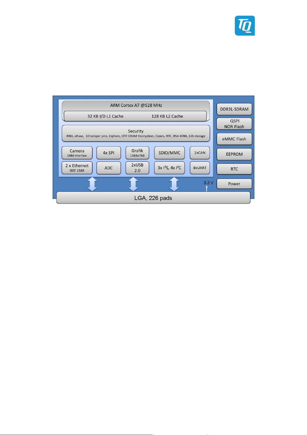
Illustration 2: Block diagram TQMa6ULxL.......................................................................................................................................................5
Illustration 3: Block diagram Boot Mode ......................................................................................................................................................... 6
Illustration 4: Position of Boot-Mode configuration DIP switches – S13, S16......................................................................................7
Illustration 5: Block diagram I2C busses ...........................................................................................................................................................8
Illustration 6: Reset and Power button – S1, S2.......................................................................................................................................... 10
Illustration 7: Block diagram USB Host interfaces...................................................................................................................................... 11
Illustration 8: Block diagram USB 2.0 Hi-Speed OTG................................................................................................................................. 12
Illustration 9: Block diagram Ethernet 100 BASE-T.................................................................................................................................... 13
Illustration 10: Block diagram CAN................................................................................................................................................................... 14
Illustration 11: Block diagram display interface, X19 .................................................................................................................................. 14
Illustration 12: Block diagram Micro SD card socket – X13 ....................................................................................................................... 16
Illustration 13: Block diagram Mini PCIe ......................................................................................................................................................... 17
Illustration 14: Block diagram of Starterkit headers – X22, X23............................................................................................................... 20
Illustration 15: Block diagram debug interfaces RS-232 / USB................................................................................................................. 21
Illustration 16: Block diagram power supply................................................................................................................................................. 22
Illustration 17: Block diagram input protection............................................................................................................................................ 22
Illustration 18: MBa6ULxL dimensions ............................................................................................................................................................ 24
Illustration 19: MBa6ULxL, revision 02xx, component placement top.................................................................................................. 25
Illustration 20: MBa6ULxL, revision 02xx, component placement bottom.......................................................................................... 25
REVISION HISTORY
Rev. Date Name Pos. Modification
0100 06.06.2018 Petz Initial release
0101 26.10.2018 Petz
Table 28
9
“Package temperature” replaced with “Case temperature”
Chapter reworked

User's Manual l MBa6ULxL UM 0101 l © 2018, TQ-Systems GmbH Page 1
1. ABOUT THIS MANUAL
1.1 Copyright and license expenses
Copyright protected © 2018 by TQ-Systems GmbH.
This User's Manual may not be copied, reproduced, translated, changed or distributed, completely or partially in electronic,
machine readable, or in any other form without the written consent of TQ-Systems GmbH.
The drivers and utilities for the components used as well as the BIOS are subject to copyrights of the respective manufacturers.
The licence conditions of the respective manufacturer are to be adhered to.
Bootloader-licence expenses are paid by TQ-Systems GmbH and are included in the price.
Licence expenses for the operating system and applications are not taken into consideration and must be calculated / declared
separately.
1.2 Registered trademarks
TQ-Systems GmbH aims to adhere to copyrights of all graphics and texts used in all publications, and strives to use original
or license-free graphics and texts.
All brand names and trademarks mentioned in this User's Manual, including those protected by a third party, unless specified
otherwise in writing, are subjected to the specifications of the current copyright laws and the proprietary laws of the present
registered proprietor without any limitation. One should conclude that brand and trademarks are rightly protected by a third
party.
1.3 Disclaimer
TQ-Systems GmbH does not guarantee that the information in this User's Manual is up-to-date, correct, complete or of good
quality. Nor does TQ-Systems GmbH assume guarantee for further usage of the information. Liability claims against TQ-Systems
GmbH, referring to material or non-material related damages caused, due to usage or non-usage of the information given in this
User's Manual, or due to usage of erroneous or incomplete information, are exempted, as long as there is no proven intentional
or negligent fault of TQ-Systems GmbH.
TQ-Systems GmbH explicitly reserves the rights to change or add to the contents of this User's Manual or parts of it without
special notification.
Important Notice:
Before using the Starterkit MBa6ULxL or parts of the schematics of the MBa6ULxL, you must evaluate it and determine if it is
suitable for your intended application. You assume all risks and liability associated with such use. TQ-Systems GmbH makes no
other warranties including, but not limited to, any implied warranty of merchantability or fitness for a particular purpose. Except
where prohibited by law, TQ-Systems GmbH will not be liable for any indirect, special, incidental or consequential loss or damage
arising from the usage of the Starterkit MBa6ULxL or schematics used, regardless of the legal theory asserted.
1.4 Imprint
TQ-Systems GmbH
Gut Delling, Mühlstraße 2
D-82229 Seefeld
Tel: +49 8153 9308–0
Fax: +49 8153 9308–4223
E-Mail:
Web:
Info@TQ-Group
TQ-Group

User's Manual l MBa6ULxL UM 0101 l © 2018, TQ-Systems GmbH Page 2
1.5 Tips on safety
Improper or incorrect handling of the MBa6ULxL can substantially reduce its life span.
1.6 Symbols and typographic conventions
Table 1: Terms and Conventions
Symbol Meaning
This symbol represents the handling of electrostatic-sensitive modules and / or components. These
components are often damaged / destroyed by the transmission of a voltage higher than about 50 V.
A human body usually only experiences electrostatic discharges above approximately 3,000 V.
This symbol indicates the possible use of voltages higher than 24 V.
Please note the relevant statutory regulations in this regard.
Non-compliance with these regulations can lead to serious damage to your health and also cause
damage / destruction of the component.
This symbol indicates a possible source of danger. Acting against the procedure described can lead to
possible damage to your health and / or cause damage / destruction of the material used.
This symbol represents important details or aspects for working with the MBa6ULxL.
Command
A font with fixed-width is used to denote commands, file names, or menu items.
1.7 Handling and ESD tips
General handling of the MBa6ULxL:
The MBa6ULxL may only be used and serviced by certified personnel who have taken note of the
information, the safety regulations in this document and all related rules and regulations.
A general rule is: do not touch the MBa6ULxL during operation. This is especially important when
switching on, changing jumper settings or connecting other devices without ensuring beforehand
that the power supply of the system has been switched off.
Violation of this guideline may result in damage / destruction of the MBa6ULxL and be dangerous
to your health.
Improper handling of your MBa6ULxL would render the guarantee invalid.
Proper ESD handling:
The electronic components of the MBa6ULxL are sensitive to electrostatic discharge (ESD).
Always wear antistatic clothing, use ESD-safe tools, packing materials etc., and operate the MBa6ULxL
in an ESD-safe environment. Especially when you switch modules on, change jumper settings, or
connect other devices.

User's Manual l MBa6ULxL UM 0101 l © 2018, TQ-Systems GmbH Page 3
1.8 Naming of signals
A hash mark (#) at the end of the signal name indicates a low-active signal.
Example: RESET#
If a signal can switch between two functions and if this is noted in the name of the signal, the low-active function is marked with
a hash mark and shown at the end.
Example: C / D#
If a signal has multiple functions, the individual functions are separated by slashes when they are important for the wiring.
The identification of the individual functions follows the above conventions.
Example: WE2# / OE#
1.9 Further applicable documents / presumed knowledge
• Specifications and manual of the modules used:
These documents describe the service, functionality and special characteristics of the module used (incl. BIOS).
• Specifications of the components used:
The manufacturer’s specifications of the components used, for example CompactFlash cards, are to be taken note of.
They contain, if applicable, additional information that must be taken note of for safe and reliable operation.
These documents are stored at TQ-Systems GmbH.
• Chip errata:
It is the user’s responsibility to make sure all errata published by the manufacturer of each component are taken note of.
The manufacturer’s advice should be followed.
• Software behaviour:
No warranty can be given, nor responsibility taken for any unexpected software behaviour due to deficient components.
• General expertise:
Expertise in electrical engineering / computer engineering is required for the installation and the use of the device.
The following documents are required to fully comprehend the following contents:
• MBa6ULxL circuit diagram
• TQMa6ULxL User's Manual
• IMX6ULRM Reference Manual
• U-Boot documentation:
• PTXdist documentation:
• TQ-Support Wiki:
www.denx.de/wiki/U-Boot/Documentation
www.ptxdist.de
support.tq-group.com/doku.php?id=en:arm:TQMa6ULx
2. BRIEF DESCRIPTION
This User's Manual describes the hardware of the MBa6ULxL, revision 02xx. The MBa6ULxL is designed as a carrier board for the
LGA version of the TQMa6ULxL. The illustrations in this User's Manual also refer to the TQMa6ULxL.
In addition the standard interfaces routed to the user’s connectors, more interfaces like CAN, UART, RS-232, GPIO, I2C and SPI
interfaces are routed to headers on the MBa6ULxL. The characteristics of the i.MX6ULx can be evaluated, and therefore the
software development can start immediately.
Currently the MBa6ULxL supports TQMa6ULxL modules with NXP i.MX6UL CPU derivatives MCIMX6G
MCIMX6G
3CVM05AA. Currently i.MX6ULL CPUs are not supported.
2CVM05AA and

User's Manual l MBa6ULxL UM 0101 l © 2018, TQ-Systems GmbH Page 4
3. TECHNICAL DATA
3.1 System architecture and functionality
3.1.1 MBa6ULxL Block diagram
USB OTG
(Micro USB)
USB HOST 1
(TypeA)
USB HOST 2
(TypeA)
Ethernet 1
(RJ45)
Ethernet 2
(RJ45)
CAN 1
(Pin header)
CAN 2
(Pin header)
USB Debug
(Micro USB)
MBa6ULxL
USB 20
Hub
USB HOST 3
(internal)
10/100 MBit
Ethernet PHY
10/100 MBit
Ethernet PHY
Battery
(CR2032)
CAN
Transceiver
CAN
Transceiver
USB
Transceiver
Galvanically
isolated
USBOTG 1
USBOTG 2
UART1 FTDI
RMII 1
RMII 2
LICELL
CAN1
CAN2
Analog
Switch
RS232.1 RS232.2
UART1
RS232
Transceiver
20pin 2.54 mm header
CSI
TQMa6ULxL
UART3
SPI
RS232
Transceiver
GPIO
I²C
Reset/PowerOn
buttons
Boot Mode
(DIP switch)
120 CAN
termination
(DIP switch)
Internal
Supply
I2C4
LCD
SDHC
USB Host 3
USB Host 4
Power supply
3.3 V / 5 V
Controller
Mini PCIe 1
Mini PCIe 2
Touch
Protective
Ciruitry
40pin.
FFC connector
SD card
socket
SIM card
socket
PowerIN
(DC socket)
20pin 2.54 mm header
Illustration 1: Block diagram MBa6ULxL
3.1.2 Functionality
Core of the MBa6ULxL is the TQMa6ULxL, which is based on an NXP i.MX6ULx CPU. In addition to the standard communication
interfaces like USB, Ethernet, RS-232, etc. other signals and interfaces are routed to two 20-pin 2.54 mm headers.
The MBa6ULxL provides the following interfaces and functions:
Table 2: Overview interfaces
Connector Interface Qty. Type of connector Remark
X1, X2 CAN 2.0B 2 Phoenix contact, MC1.5/3-G-3.5 CAN transceiver, galvanically separated
X10 USB / RS-232 1 Single USB receptacle Micro-AB RS-232 debug interface (via FTDI as USB)
X12 SIM card 1 SIM card socket –
X13 SD card 1 Micro SD card connector –
X14 Ethernet 2 RJ45 receptacle 10/100BASE-T, double RJ45 with integrated magnetics
X15 USB-OTG 1 Single USB receptacle Micro-AB USB OTG
X16 USB Host 2 Stacked USB receptacle Type-A USB Host 1 / 2
X19 Graphics 1 40-pin FFC, 0.5 mm Meets EDT platform concept, for displays with PCT or RT
X21 Power 1 Phoenix contact, MC1,5/2-G-3,5 Power supply 6.5 V to 30 V
X22 GPIOs 1 20-pin header, 2.54 mm pitch I2C4, SPI2, RS-232.1, RS-232.2, PWM, Ext-Wakeup, 2 x ADC, 3.3 V, 5.0 V
X23 GPIOs 1 20-pin header, 2.54 mm pitch GPIOS, I2C2, UART6, 3.3 V, 5.0 V
X24 Mini PCIe 1 Mini PCIe connector LoRa (assembly option)
X25 Mini PCIe 1 Mini PCIe connector Mini PCIe (only USB), with SIM card socket (assembly option)
G2 Battery 1 SMTU2032 Battery / GoldCap for RTC
User's Manual l MBa6ULxL UM 0101 l © 2018, TQ-Systems GmbH Page 5
4. ELECTRONICS
4.1 System components
4.1.1 TQMa6ULxL
Illustration 2: Block diagram TQMa6ULxL
The TQMa6ULxL with the i.MX6ULx CPU is the central system component. It provides DDR3L SDRAM, eMMC, NOR flash and
EEPROM memory. All voltages required by the TQMa6ULxL are derived from the supply voltage. More information is to be taken
from the accompanying User’s Manual of the TQMa6ULxL (7).
The boot behaviour of the TQMa6ULxL can be customised. The required Boot-Mode configuration can be set with DIP switches
on the MBa6ULxL, see chapter 4.1.2.

User's Manual l MBa6ULxL UM 0101 l © 2018, TQ-Systems GmbH Page 6
4.1.2 Boot-Mode configuration
The TQMa6ULxL can boot from different media:
• eMMC (on TQMa6ULxL)
• QSPI NOR flash
• SD card
The settings of DIP switches S13 and S16 determine, which device is selected to boot from.
Illustration 3: Block diagram Boot Mode
Attention: Flickering display
During the boot process, the LCD_DATA signals are not separated from the display. It may therefore
be necessary to deactivate the display at system start-up. This can be implemented by appropriate
software adaptation via the Data Enable Input.

User's Manual l MBa6ULxL UM 0101 l © 2018, TQ-Systems GmbH Page 7
The following tables describe the DIP switch settings for each boot source.
Further settings such as transfer modes and CPU clock are to be taken from the TQMa6ULxL User's Manual (7).
Table 3: Boot-Mode configuration
Boot-Mode S13-2, BOOT_MODE1 S13-1, BOOT_MODE0
Boot from eFuses OFF OFF
Serial Downloader OFF ON
Internal Boot ON OFF
Reserved ON ON
Table 4: Boot-Mode configuration DIP switches – S13, S16
DIP switch eMMC SD card QSPI NOR Serial-Downloader
S13
1 OFF OFF OFF ON
2 ON ON ON OFF
1 X X X X
2 ON OFF X X
3 OFF ON X X
S16
4 ON OFF X X
5 ON ON OFF X
6 ON OFF OFF X
7 OFF OFF ON X
8 OFF ON OFF X
Illustration 4: Position of Boot-Mode configuration DIP switches – S13, S16

User's Manual l MBa6ULxL UM 0101 l © 2018, TQ-Systems GmbH Page 8
4.1.3 I
2
C address mapping
A port replicator and the I2C touch screen controller can be addressed via I2C4 on the MBa6ULxL.
Table 5 shows the addresses used on the TQMa6ULxL and the MBa6ULxL. The I2C4 bus is also routed to header X22.
The following table shows the address assignment of TQMa6ULxL and MBa6ULxL.
Illustration 5: Block diagram I2C busses
Table 5: I2C4 address assignment
Component Ref ID Address Location
PMIC (PF3000/3001) –
Temperature sensor (SE97BTP) –
Port replicator (PCA9554BS) D20
I2C Touch Screen Controller (STMPE811Q) D9
EEPROM (24LC64T-I_MC) –
EEPROM (SE97BTP) –
EEPROM (SE97BTP) –
RTC (DS1339U-33) –
0x08 000 1000b
0x1A 001 1010b
0x22 010 0010b
0x41 100 0001b
0x50 101 0000b
0x32 011 0010b
0x52 101 0010b
0x68 110 1000b
TQMa6ULxL
TQMa6ULxL
MBa6ULxL
MBa6ULxL
TQMa6ULxL
TQMa6ULxL
TQMa6ULxL
TQMa6ULxL

User's Manual l MBa6ULxL UM 0101 l © 2018, TQ-Systems GmbH Page 9
4.1.4 Port replicator PCA9554BS signals
The port replicator PCA9554BS with I2C address 0x22 provides the following signals:
Table 6: Port replicator PCA9554BS signals
I/O port Direction Function Remark
IO0 O ENET1_RST# –
IO1 O ENET2_RST# –
IO2 O BOOT_CFG_EN# –
IO3
IO4
O PWR_EN_3V3_DISPLAY Default
I ENET1_INT# Alternative
O PWR_EN_1V5 Default
I ENET2_INT# Alternative
IO5 O LCD.PWRCTRL –
IO6 O LCD.WAKE –
IO7 O PCIE_1.DIS# Alternative: PCIE_2.DIS#
Attention: I2C4 bus
Attention when using I2C4. Since the PMIC can be addressed via I2C4,
errors on the bus can lead to instabilities of the MBa6ULxL!
4.1.5 Temperature sensor / SPD EEPROM
Since there is already a temperature sensor SE97BTP on the TQMa6ULxL, no temperature sensor is provided on the MBa6ULxL.
4.1.6 RTC supply
The TQMa6ULxL provides a discrete RTC. Another RTC is provided by the i.MX6ULx on the TQMa6ULxL.
Both RTCs are supplied via the LICELL.
A lithium battery type CR2032 with very low self-discharge is provided on the MBa6ULxL as a backup supply for both RTCs.
The increased current consumption must be considered, if the i.MX6ULx RTC is used.
This leads to a fast battery discharge. More information can be found in the User’s Manual of the TQMa6ULxL.
For the RTCs installed on the MBa6ULxL the following applies:
Table 7: RTC supply, components
Parameter Value Remark
Coin cell 2.1 V to 3.7 V, typical 3.0 V, 220 mAh –20 °C to +60 °C
Current consumption RTC See TQMa6ULxL User’s Manual Depends on RTC used

User's Manual l MBa6ULxL UM 0101 l © 2018, TQ-Systems GmbH Page 10
4.1.7 Reset and Power
The MBa6ULxL provides a power and a reset button. Signal RESET_OUT# resets all components on the MBa6ULxL.
The following table shows the signals.
Table 8: TQMa6ULxL Reset and power-on signals
Push button Signal TQMa6ULxL pad Direction Remark
S1 RESET_IN# T14 I 10 kΩ PU to 3.3 V on MBa6ULxL
S2 PMIC_PWRON U16 I 10 kΩ PU to 3.3 V on MBa6ULxL
– RESET_OUT# U15 O Resets all components on MBa6ULxL
RESET_IN#
PMIC_PWRON
TQMa6ULxL
RESET_OUT#
Push button S1
Push button S2
[System]
Illustration 6: Reset and Power button – S1, S2
4.1.8 Status LED
The MBa6ULxL provides a status LED. The LED shines green during normal operation and orange during reset.
User's Manual l MBa6ULxL UM 0101 l © 2018, TQ-Systems GmbH Page 11
4.2 Communication interfaces
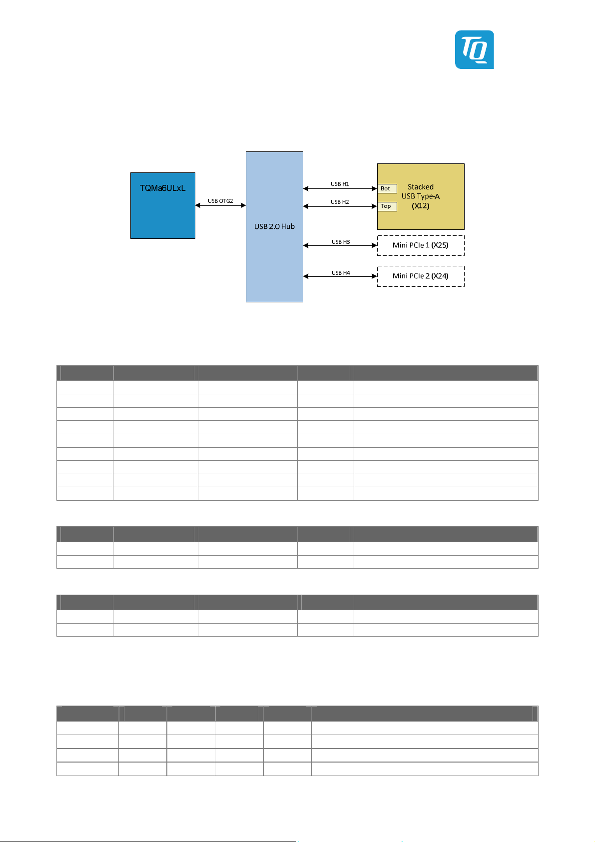
4.2.1 USB 2.0 Hi-Speed Host
The MBa6ULxL provides two USB 2.0 Host (double stack USB Type-A) and USB 2.0 Host interfaces at both Mini PCIe connectors.
Illustration 7: Block diagram USB Host interfaces
The following tables show the pinout of the connectors used.
Table 9 Pinout USB Host 1 & 2, stacked USB Type-A – X12
Pin Pin name Signal Direction Remark
1A VBUS USB_H1_VBUS P 100 µF to DGND + EMI Filter
2A D– USB_H1_D_N I/O Common Mode Choke in series
3A D+ USB_H1_D_P I/O Common Mode Choke in series
4A DGND DGND P –
1B VBUS USB_H2_VBUS P 100 µF to DGND + EMI Filter
2B D– USB_H2_D_N I/O Common Mode Choke in series
3B D+ USB_H2_D_P I/O Common Mode Choke in series
4B DGND DGND P –
M1 – M4 DGND DGND P –
Table 10 Pinout USB Host 3, Mini PCIe 1 – X25
Pin Pin name Signal Direction Remark
36 D– USB_H3_D_N I/O Common Mode Choke in series
38 D+ USB_H3_D_P I/O Common Mode Choke in series
Table 11 Pinout USB Host 4, Mini PCIe 2 – X24
Pin Pin name Signal Direction Remark
36 D– USB_H4_D_N I/O Common Mode Choke in series
38 D+ USB_H4_D_P I/O Common Mode Choke in series
The USB host port of the TQMa6ULxL provides a theoretical data rate of 480 Mbit/s. The data rate is shared amongst the
connected ports. The data rates of the ports can significantly deviate depending on the hardware and software used.
Table 12: Characteristics USB
Parameter Min. Typ. Max. Unit Remark
Voltage 4.75 5 5.25 V –
Current – 500 900 mA –
Read – 15.7 – Mbyte/s USB stick at port 1: 100 Mbyte file, 10 Mbyte block size
Write – 7.4 – Mbyte/s USB stick at port 1: 100 Mbyte file, 10 Mbyte block size

User's Manual l MBa6ULxL UM 0101 l © 2018, TQ-Systems GmbH Page 12
4.2.2 USB 2.0 Hi-Speed OTG
Both USB-OTG interfaces of the TQMa6ULxL are provided on the MBa6ULxL.
USB-OTG1 is provided at a 5-pin Micro-AB receptacle. USB-OTG2 is connected to the USB hub controller, see 4.2.1.
Both OTG interfaces operate in host mode only.
An OTG or device function is not implemented in software except for the serial downloader.
Illustration 8: Block diagram USB 2.0 Hi-Speed OTG
The following table shows the pinout of the connector used.
Table 13: Pinout USB-Host OTG – X15
Pin Pin name Signal Direction Remark
1 VBUS USB_OTG2_VBUS P 100 µF to DGND; EMI filter, I
= 100 mA
max
2 D– USB_OTG2_D_N I/O Common mode choke in series
3 D+ USB_OTG2_D_P I/O Common mode choke in series
4 ID USB_OTG2.ID I –
5 DGND DGND P –
M1 – M6 DGND DGND P –
The interface can serve as Client or Host. To use this feature, appropriate software support is necessary, however.
The OTG ports of the TQMa6ULxL provide a theoretical data rate of 480 Mbit/s. The data rate can significantly deviate depending
on the hardware and software used.
Table 14: Characteristics USB 2.0 Hi-Speed OTG
Parameter Min. Typ. Max. Unit Remark
Voltage 4.75 5 5.25 V –
Current – 500 900 mA –
Read – 20.4 – Mbyte/s USB 2.0 stick: 100 Mbyte file, 10 Mbyte block size
Write – 8.0 – Mbyte/s USB 2.0 stick: 100 Mbyte file, 10 Mbyte block size

User's Manual l MBa6ULxL UM 0101 l © 2018, TQ-Systems GmbH Page 13
4.2.3 Ethernet
Both i.MX6ULx MACs are provided on the MBa6ULxL via two SMSC PHYs LAN8720Ai. The PHYs are connected via RMII.
The implementation is shown in the following block diagram.
Illustration 9: Block diagram Ethernet 100 BASE-T
Both RJ45 jacks contain integrated magnetics and two status LEDs.
The following tables show the pinout of the RJ45 receptacles.
Table 15: Pinout Ethernet 1 – X14, left
Pin Pin name Signal Direction
1 TX+ ETH1_MDI_TX_P I/O
2 TX– ETH1_MDI_TX_N I/O
3 RX+ ETH1_MDI_RX_P I/O
4 – NC –
5 – NC –
6 RX– ETH1_MDI_RX_N I/O
7 – NC –
8 – NC –
Table 16: Pinout Ethernet 2 – X14, right
Pin Pin name Signal Direction
1 TX+ ETH2_MDI_TX_P I/O
2 TX– ETH2_MDI_TX_N I/O
3 RX+ ETH2_MDI_RX_P I/O
4 – NC –
5 – NC –
6 RX– ETH2_MDI_RX_N I/O
7 – NC –
8 – NC –
The possible data throughput is influenced by the system load and the software platform used.

User's Manual l MBa6ULxL UM 0101 l © 2018, TQ-Systems GmbH Page 14
4.2.4 CAN
The MBa6ULxL provides two CAN interfaces. CAN1 is routed to X1, CAN2 is optionally available at X2.
Both interfaces are galvanically separated. The CAN interfaces are not separated galvanically among themselves.
The CAN signals can be terminated with 120 Ω using DIP switches S15 and S14.
Illustration 10: Block diagram CAN
Table 17: Pinout CAN1, CAN2 – X1, X2
Connector Pin Pin name Signal Direction Termination Remark
1 CAN_H CAN2_P I/O S15-2
X1
2 CAN_L CAN2_N I/O S15-1
Assembled
3 DGND DGND_CAN P –
1 CAN_H CAN1_P I/O S14-2
X2
2 CAN_L CAN1_N I/O S14-1
Optionally
available
3 DGND DGND_CAN P –
4.2.5 Display interface
The i.MX6ULx provides an Enhanced LCD Interface (eLCDIF), which is routed to X19 on the MBa6ULxL. The eLCDIF consists of
24 data and 5 control signals and supports different video formats like RGB, VSYNC, ITU-R BT.656, or 4:2:2 YCbCr.
The following block diagram shows the display interface:
Illustration 11: Block diagram display interface, X19

User's Manual l MBa6ULxL UM 0101 l © 2018, TQ-Systems GmbH Page 15
The following table shows the pinout of connector X19.
Table 18: Pinout LCD interface, X19
Pin Signal TQMa6ULxL LCD channel RGB Remark
1 TOUCH_X– – – –
2 TOUCH_Y– – – Optional I2C4 SDA
3 TOUCH_X+ – – –
4 TOUCH_Y+ – – Optional I2C4 CLK
5 LED_CTRL – – –
6 TOUCH_INT# – – –
7 VCC3V3 – – Backlight VCC
8 VCC3V3 – – Backlight VCC
9 GND – – –
10 GND – – –
11 VCC3V3 – – Digital VDD
12 LCD_PWR_CTRL – – 3.3 V
13 LCD_ENABLE U2 – 3.3 V
14 LCD_VSYNC U4 – 3.3 V
15 LCD_HSYNC U3 – 3.3 V
16 LCD_WAKE – – 3.3 V
17 LCD_CLK T1 – 3.3 V
18 GND – – –
19 LCD_DATA18 K3 R2 (LSB) –
20 LCD_DATA19 K4 R3 –
21 LCD_DATA20 J1 R4 –
22 LCD_DATA21 J2 R5 –
23 LCD_DATA22 J3 R6 –
24 LCD_DATA23 J4 R7 (MSB)
25 GND – – –
26 LCD_DATA10 M1 G2 (LSB) –
27 LCD_DATA11 M3 G3 –
28 LCD_DATA12 M4 G4 –
29 LCD_DATA13 L1 G5 –
30 LCD_DATA14 L2 G6 –
31 LCD_DATA15 L3 G7 (MSB)
32 GND – – –
33 LCD_DATA2 R3 B2 (LSB) –
34 LCD_DATA3 P1 B3 –
35 LCD_DATA4 P3 B4 –
36 LCD_DATA5 P4 B5 –
37 LCD_DATA6 N1 B6 –
38 LCD_DATA7 N2 B7 (MSB)
39 LCD_RESET# T4 – 3.3 V
40 LCD.RESET# – – Not connected, optional
–
–
–
FFC connector type Hirose FH12A-40S-0.5SH (55) is assembled on the MBa6ULxL.
4.2.6 Touch controller
The i.MX6ULx Touch Screen Controller (TSC) signals are used for USB OTG. Therefore a separate TSC STMPE811 is assembled on
the MBa6ULxL. The STMPE811 is connected to I2C4 using address 0x41.
4.2.7 Backlight control
Attention, TBD: The display brightness can be controlled at pin X19-5 with PWM signal PWM4 (TQMa6ULxL, pad H15).

User's Manual l MBa6ULxL UM 0101 l © 2018, TQ-Systems GmbH Page 16
4.2.8 Micro SD card connector
The Micro SD card connector is connected to the USDHC1 controller on the TQMa6ULxL with a 4-bit wide data interface.
3.3 V are provided at the Micro SD card connector. All data lines provide ESD protection.
All signals except CLK are pulled-up to 3.3 V with 10 kΩ. Write Protection (WP) is not available.
Booting from Micro SD card is possible (see chapter 4.1.2).
Illustration 12: Block diagram Micro SD card socket – X13
The read and write speeds of the Micro SD card interface depend on the Micro SD card used.
The following table shows the pinout of Micro SD card connector X13:
Table 19: Pinout Micro SD card socket – X13
Pin Signal Remark
1 USDHC1.DAT2 10 kΩ Pull-Up to VCC3V3 + ESD protection
2 USDHC1.DAT3 10 kΩ Pull-Up to VCC3V3 + ESD protection
3 USDHC1.CMD 10 kΩ Pull-Up to VCC3V3 + ESD protection
4 VDD 3.3 V
5 USDHC1.CLK ESD protection
6 DGND Ground
7 USDHC1.DAT0 10 kΩ Pull-Up to VCC3V3 + ESD protection
8 USDHC1.DAT1 10 kΩ Pull-Up to VCC3V3 + ESD protection
SW1 USDHC1.CD# 10 kΩ Pull-Up to VCC3V3 + ESD protection
M1, M2, M3, M4 DGND SHIELD

User's Manual l MBa6ULxL UM 0101 l © 2018, TQ-Systems GmbH Page 17
4.2.9 Mini PCIe and SIM card socket
Two Mini PCIe connectors for full-size Mini PCIe cards (50.95 × 30 mm) are provided on the MBa6ULxL.
Every standard Mini PCIe card can be used 1. USB_H3, USB_H4, and I2C4 are routed to the connectors, see Table 21.
A SIM card socket to connect an UMTS / GSM modem is available.
The following block diagram shows the interfaces to Mini PCIe 1 and Mini PCIe 2.
Illustration 13: Block diagram Mini PCIe
The maximum load on the voltages provided for the Mini PCIe card is given in the following table.
Table 20: Current load Mini PCIe
Parameter I
Mini PCIe 1 I
max
Mini PCIe 2 Remark
max
Current @ 1.5 V 0.375 A 0.375 A –
Current @ 3.3 V 1.1 A 1.1 A Default
Current @ 5 V 0.8 A 2.0 A Assembly option
Note: 5 V SIM card
SIM cards, which require a 5 V supply, are only supported by assembly option.
Note: Space between PCB and PCIe card
The space between PCB and PCIe card has to be taken into account!
1: If suitable Mini PCIe card driver software is provided.

User's Manual l MBa6ULxL UM 0101 l © 2018, TQ-Systems GmbH Page 18
The following table shows the pinout of Mini PCIe connectors and SIM Card socket.
Table 21: Pinout Mini PCIe – X24, X25; SIM card socket – X12
Mini PCIe pin Mini PCIe 2, X24 Mini PCIe 1, X25 SIM card, X12 Remark
1 NC NC – –
2 VCC_MPCIE2 VCC_MPCIE1 – Default 3.3 V, optional 5 V, see Table 20
3 NC NC – –
4 DGND DGND – –
5 NC NC – –
6 VCC1V5 VCC1V5 – See Table 20
7 NC NC – –
8 NC SIM_PWR SIM_PWR X12-C1, see Table 22
9 DGND DGND – –
10 NC SIM_DATA SIM_DATA X12-C7, see Table 22
11 NC NC – –
12 NC SIM_CLK SIM_CLK X12-C3, see Table 22
13 NC NC – –
14 NC SIM_RST SIM_RST X12-C2, see Table 22
15 DGND DGND – –
16 NC SIM_VPP SIM_VPP X12-C6, see Table 22
17 NC NC – –
18 DGND DGND – –
19 NC NC – –
20 PCIE_2.DIS# PCIE_1.DIS# – –
21 DGND DGND – –
22 PCIE_RST# PCIE_RST# – –
23 NC, optional 5 V NC – –
24 VCC_MPCIE2 VCC_MPCIE1 – Default 3.3 V, optional 5 V, see Table 20
25 NC, optional 5 V NC – –
26 DGND DGND – –
27 DGND DGND – –
28 VCC1V5 VCC1V5 – See Table 20
29 DGND DGND – –
30 I242.SCL I242.SCL – –
31 NC NC – –
32 I2C4.SDA I2C4.SDA – For I2C4 address mapping see Table 5
33 NC NC – –
34 DGND DGND – –
35 DGND DGND – –
36 USB_H4_D_N USB_H3_D_N – Common mode choke in series
37 DGND DGND – –
38 USB_H4_D_P USB_H3_D_P – Common mode choke in series
39 VCC_MPCIE2 VCC_MPCIE1 – Default 3.3 V, optional 5 V, see Table 20
40 DGND DGND – –
41 VCC_MPCIE2 VCC_MPCIE1 – Default 3.3 V, optional 5 V, see Table 20
42 NC NC – –
43 DGND DGND – –
44 NC NC – –
45 NC NC – –
46 NC NC – –
47 NC NC – –
48 VCC1V5 VCC1V5 – See Table 20
49 NC NC – –
50 DGND DGND – –
51 NC NC – –
52 VCC_MPCIE2 VCC_MPCIE1 – Default 3.3 V, optional 5 V, see Table 20
User's Manual l MBa6ULxL UM 0101 l © 2018, TQ-Systems GmbH Page 19
4.2.10 SIM card socket
The following table shows the pinout of the SIM card socket.
Table 22: Pinout SIM card socket – X12
Pin Signal Remark
C1 SIM_PWR –
C2 SIM_RST –
C3 SIM_CLK –
C4 NC Reserved
C5 DGND –
C6 SIM_VPP –
C7 SIM_DATA –
C8 NC Reserved
DC NC D-Contact
DS NC D-Spring
GND Ground –

User's Manual l MBa6ULxL UM 0101 l © 2018, TQ-Systems GmbH Page 20
4.2.11 20-pin headers
The MBa6ULxL is equipped with two 20-pin headers with 2.54 mm pitch.
3.3 V, 5 V, SPI, I2C4, ADC
UART 1
UART 3
RS232
Transceiver
RS232
Transceiver
RS232_1
RS232_2
Header 1 (X22)
TQMa6ULxL
CMOS Sensor Interface (CSI)
3.3 V, 5 V, UART, I2C2, GPIO
Header 2 (X23)
Illustration 14: Block diagram of Starterkit headers – X22, X23
Table 23: Pinout header 1 – X22
Alternative Default Pin Default Alternative
5 V 1 2 3.3 V
GND 3 4 GND
UART4_TX SPI2_SCLK 5 6 I2C4_SCL –
UART4_RX SPI2_SS0# 7 8 I2C4_SDA –
UART5_RX SPI2_MISO 9 10 TOUCH_INT# ADC_1
UART5_TX SPI2_MOSI 11 12 GPIO1_IO02 ADC_2
GND 13 14 GND
– RS-232_1_TX 15 16 RS-232_2_TX –
– RS-232_1_RX 17 18 RS-232_2_RX –
LCD_DATA17 EXT_WAKEUP 19 20 PWM2 GPIO1_IO09
Table 24: Pinout header 2 – X23
Alternative Default Pin Default Alternative
5 V 1 2 3.3 V
GND 3 4 GND
CSI_DATA04 GPIO4_IO25 5 6 GPIO4_IO21 CSI_DATA00
CSI_DATA05 GPIO4_IO26 7 8 GPIO4_IO22 CSI_DATA01
CSI_DATA06 GPIO4_IO27 9 10 GPIO4_IO23 CSI_DATA02
CSI_DATA07 GPIO4_IO28 11 12 GPIO4_IO24 CSI_DATA03
GND 13 14 GND
CSI_MCLK UART6_TX 15 16 I2C2_SCL CSI_HSYNC / UART6_CTS
CSI_PIXCLK UART6_RX 17 18 I2C2_SDA CSI_VSYNC / UART6_RTS
GND 19 20 GND

User's Manual l MBa6ULxL UM 0101 l © 2018, TQ-Systems GmbH Page 21
4.3 Diagnostic- and user interfaces
4.3.1 Power-On and Reset-button
See chapter 4.1.7.
4.3.2 CAN termination
See chapter 4.2.4.
4.3.3 Debug interfaces RS-232 / USB
Debug interfaces are available as RS-232 and USB device interface on the MBa6ULxL.
In both cases, the UART1 interface of the TQMa6ULxL is used. No software configuration is required.
DIP switch S16-1 selects the debug interface, see Table 26.
Illustration 15: Block diagram debug interfaces RS-232 / USB
Table 23 shows the pinout of the RS-232 signals. The following table shows the pinout of debug Micro USB connector X10.
Table 25: Pinout debug USB – X10
Pin Pin name Signal Direction Remark
1 VBUS_SENSE VBUS_SENSE – –
2 USB_D_N USB_RS-232_D_N I/O –
3 USB_D_P USB_RS-232_D_P I/O –
4 – NC – Not used
5 DGND DGND P –
M1 – M6 Shield DGND P –
Table 26: Debug interface selection – S16-1
DIP switch On Off
S16-1 Debug-Interface RS-232 at X22 Debug-Interface USB device at X10

User's Manual l MBa6ULxL UM 0101 l © 2018, TQ-Systems GmbH Page 22
4.4 Power supply
The MBa6ULxL is supplied with 6.5 to 30 V via X26 or X27. All other voltages are generated on the MBa6ULxL.
Additionally, 3.3 V and 5 V are available at headers X22 and X23.
The Mini PCIe connectors X24 and X25 are supplied with 1.5 V and 3.3 V.
A 5 V supply instead of 3.3 V is possible as assembly option.
Illustration 16: Block diagram power supply
4.4.1 Protective circuitry
The MBa6ULxL can be supplied with 6.5 V to 30 V DC. The protective circuit has the following characteristics:
• Slow blow fuse 5 A
• Excess voltage protection diode
• PI filter
• Inverse-polarity protection
Illustration 17: Block diagram input protection
4.4.2 Power consumption
The typical power consumption of the MBa6ULxL without display is approximately 3 ~ 4 W.
If however a display is powered by the MBa6ULxL, the power consumption depends on the display connected.
4.4.3 Power supply connector
A 2-pin Phoenix connector type MC 1,5/2-G-3,5 is assembled on the MBa6ULxL.
Suitable mating connectors are e.g., Phoenix Contact
• Part Number 1840366 (Screw Terminals)
• Part Number 1952267 (Push-In Spring)

User's Manual l MBa6ULxL UM 0101 l © 2018, TQ-Systems GmbH Page 23
5. SOFTWARE
The following table provides an overview of the implemented software interfaces:
Table 27: Software interfaces
Device Function Supported Linux
Resolutions: from 800 × 480
i.MX6UL Display
i.MX6UL Backlight TBD yes
i.MX6UL
I2C Port - ADC
Touch
i.MX6UL DDR3L Bus width: 16 bit yes
i.MX6UL SPI NOR flash Bootable: yes yes
i.MX6UL eMMC Flash Bootable: yes yes
i.MX6UL COM ports
i.MX6UL I2C Ports EEPROM (24LC64T) yes
i.MX6UL I2C Ports RTC yes
i.MX6UL I2C Ports Temp (LM73CIMK-0) yes
i.MX6UL RTC TBD if applicable external yes
i.MX6UL SD/SDIO
i.MX6UL USB 1 Host Hi Speed
i.MX6UL USB OTG Hi Speed / FS
Audio Line out (optional) No
Audio Line In (optional) No
Audio MIC-IN (optional) No
Audio Mixer (optional) No
i.MX6UL Ethernet 1 /2 10/100 Mbit
i.MX6UL CAN
i.MX6UL SPI As generic interface
i.MX6UL Basic Power Management Power Modes: WAIT, STOP
Colour depth: 24 bit, 24 bit RGB interface
HDMI (standard monitor)
Resolutions: TBD
Preset default calibration data
Calibration tool
Wake-up on touch event
UARTx (RS-232)
Baud rates: 9600 to 115200 Baud
Parameters: 8 N 1
Flow Control: Software & Hardware
Debug / Bootloader
SD Card Interface
Hot Plug: yes
Bootable: yes
HID-Support: Keyboard, Mouse
Mass-Storage-Support: USB-Sticks & -Hard disks
As USB Host
HID-Support: Keyboard, Mouse
Mass-Storage-Support: USB-Sticks & -Hard disks
Speeds: 10/100 Mbit/s
Duplex-Modes: Half- & Full-Duplex
Auto-Negotiation: Yes
Manual Configuration: Yes
Protocols: IP, TCP, UDP, ICMP, IEEE1588
Misc.: DHCP-Client
2 × CAN Interface
Driver: Socket-CAN
Baud rates: TBD
Protocol-Stacks: TBD (e.g., CANopen)
yes
yes
yes
yes
yes
yes
Yes
Yes

User's Manual l MBa6ULxL UM 0101 l © 2018, TQ-Systems GmbH Page 24
6. MECHANICS
6.1 Dimensions
The design of the MBa6ULxL is based on the Mini-ITX form factor (100 × 100 mm2). The MBa6ULxL provides for 4.3 mm mounting
holes. The Intel® specifications of the NUC form factor were also taken into account. The MBa6ULxL has a maximum height of
approximately 22 mm and weighs approximately 94 grams, including CR2032 battery.
Illustration 18: MBa6ULxL dimensions
6.2 Thermal management
No special precautions were taken concerning the thermal management of the MBa6ULxL. A maximum of 5 W, including
TQMa6x, have to be dissipated. More information is to be taken from the TQMa6ULxL User's Manual.
Attention: Destruction or malfunction
The i.MX6ULx belongs to a performance category in which a cooling system is essential in most
applications. It is the sole responsibility of the user to define a suitable cooling method depending on
the specific mode of operation (e.g., dependence on clock frequency, stack height, airflow, and
software).
Particularly the tolerance chain (PCB thickness, board curvature, BGA balls, BGA package, thermal pad,
heatsink) must be ensured when connecting the heat sink. The CPU is not necessarily the highest
component. Inadequate cooling connections can lead to overheating of the TQMa6ULxL and thus
malfunction, deterioration or destruction.

User's Manual l MBa6ULxL UM 0101 l © 2018, TQ-Systems GmbH Page 25
6.3 Assembly
Illustration 19: MBa6ULxL, revision 02xx, component placement top
Illustration 20: MBa6ULxL, revision 02xx, component placement bottom

User's Manual l MBa6ULxL UM 0101 l © 2018, TQ-Systems GmbH Page 26
7. SAFETY REQUIREMENTS AND PROTECTIVE REGULATIONS
7.1 EMC
An EMC test of the board alone is not intended, as it is not meaningful for the customer's application, as the passing of these
tests is essentially determined by the installation situation, wiring, operating state, design of the housing, etc.
During development, however, care was taken to avoid or filter potential sources of interference on the TQMa6ULxL as far as
possible.
7.2 ESD
Most of the interfaces on the MBa6ULxL are protected against electrostatic discharge.
7.3 Operational safety and personal security
Due to the occurring voltages (≤30 V DC), tests with respect to the operational and personal safety have not been carried out.
The superior overall system in connection with the MBa6ULxL is defined by the end customer.
8. CLIMATIC AND OPERATIONAL CONDITIONS
The MBa6ULxL is designed as an industrial single-board PC that meets all industry standards. Special attention was paid to the
temperature range from –40 °C to +85 °C. The possible temperature range strongly depends on the installation situation (heat
dissipation via the housing), so no fixed value can be specified for the entire assembly. A cooling system is essential in most
applications. It is the user’s sole responsibility to define a suitable heat sink (weight and mounting position) depending on the
specific mode of operation (e.g., dependence on clock frequency, stack height, airflow, and software). Inadequate cooling
connections can lead to overheating of the MBa6ULxL and thus malfunction, deterioration or destruction.
In general, reliable operation is possible when the following conditions are met:
Table 28: Climatic and operational conditions MBa6ULxL, extended temperature range
Parameter Range Remark
Chip temperature i.MX6 –40 °C to +95 °C Without Lithium battery CR2032
Case temperature other ICs –40 °C to +85 °C Without Lithium battery CR2032
Case temperature DDR3L SDRAM –40 °C to +95 °C Without Lithium battery CR2032
Relative air humidity (operation / storing) 10 % to 90 % Not condensing
8.1 Protection against external effects
Protection class IP00 was defined for the MBa6ULxL. There is no protection against foreign objects, touch or humidity.
8.2 Reliability and service life
The MBa6ULxL is maintenance-free. It is designed for a service life of 10 years and also to be insensitive to shock and vibration.

User's Manual l MBa6ULxL UM 0101 l © 2018, TQ-Systems GmbH Page 27
9. ENVIRONMENT PROTECTION
9.1 RoHS
The MBa6ULxL is manufactured RoHS compliant.
• All components and assemblies are RoHS compliant
• The soldering processes are RoHS compliant
9.2 WEEE
The final distributor is responsible for compliance with the WEEE® regulation.
Within the scope of the technical possibilities, the MBa6ULxL was designed to be recyclable and easy to repair.
9.3 REACH®
The EU-chemical regulation 1907/2006 (REACH® regulation) stands for registration, evaluation, certification and restriction of substances SVHC
(Substances of very high concern, e.g., carcinogen, mutagen and/or persistent, bio accumulative and toxic). Within the scope of this juridical
liability, TQ-Systems GmbH meets the information duty within the supply chain with regard to the SVHC substances, insofar as suppliers inform
TQ-Systems GmbH accordingly.
9.4 EuP
The Ecodesign Directive, also Energy using Products (EuP), is applicable to products for the end user with an annual quantity >200,000. The
MBa6ULxL must therefore always be seen in conjunction with the complete device.
The available standby and sleep modes of the components on the MBa6ULxL enable compliance with EuP requirements for the MBa6ULxL.
9.5 Packaging
By environmentally friendly processes, production equipment and products, we contribute to the protection of our environment. To be able to
reuse the MBa6ULxL, it is produced in such a way (a modular construction) that it can be easily repaired and disassembled. The energy
consumption of this subassembly is minimised by suitable measures. The MBa6ULxL is delivered in reusable packaging.
9.6 Batteries
9.6.1 General notes
Due to technical reasons a battery is necessary for the MBa6ULxL. Batteries containing mercury (Hg), cadmium (Cd) or lead (Pb) are not used.
If this is for technical reasons unavoidable, the device is marked with the corresponding hazard note.
To allow a separate disposal, batteries are generally only mounted in sockets.
9.6.2 Lithium batteries
The requirements concerning special provision 188 of the ADR (section 3.3) are complied with for Lithium batteries.
There is therefore no classification as dangerous goods:
• Basic lithium content per cell not more than 1 grams
• Basic lithium content per battery not more than 2grams
• Lithium cells and batteries are examined according to UN document ST/SG/AC.10-1.
During transport a short circuit or discharging of the socketed lithium battery is prevented by extricable insulating foils or by other suitable
insulating measures.
9.7 Other entries
By environmentally friendly processes, production equipment and products, we contribute to the protection of our environment. To be able to
reuse the MBa6ULxL, it is produced in such a way, that it can be easily repaired and disassembled. The energy consumption of this subassembly
is minimised by suitable measures. Due to the fact that at the moment there is still no technical equivalent alternative for printed circuit boards
with bromine-containing flame protection (FR-4 material), such printed circuit boards are still used. No use of PCB containing capacitors and
transformers (polychlorinated biphenyls). These points are an essential part of the following laws:
• The law to encourage the circular flow economy and assurance of the environmentally acceptable removal of waste as at 27.9.94
• Regulation with respect to the utilization and proof of removal as at 1.9.96
• Regulation with respect to the avoidance and utilization of packaging waste as at 21.8.98
• Regulation with respect to the European Waste Directory as at 1.12.01
®
(except for lithium ion and lithium polymer cells for which a lithium content of not more than 1.5 g per cell applies (equals 5 Ah)).
(except for lithium ion batteries for which a lithium content of not more than 8 grams per cell applies (equals 26 Ah)).
(Source of information: BGBl I 1994, 2705)
(Source of information: BGBl I 1996, 1382, (1997, 2860))
(Source of information: BGBl I 1998, 2379)
(Source of information: BGBl I 2001, 3379)

User's Manual l MBa6ULxL UM 0101 l © 2018, TQ-Systems GmbH Page 28
10. APPENDIX
10.1 Acronyms and definitions
The following acronyms and abbreviations are used in this document:
Table 29: Acronyms
Acronym Meaning
ADC Analog/Digital Converter
BGA Ball Grid Array
BIOS Basic Input/Output System
CAN Controller Area Network
CPU Central Processing Unit
DDR3L Double Data Rate 3 Low voltage
DHCP Dynamic Host Configuration Protocol
DIP Dual In-line Package
EDT Emerging Display Technology
EEPROM Electrically Erasable Programmable Read-only Memory
EMC Electromagnetic Compatibility
EMI Electromagnetic Interference
eMMC embedded Multimedia Card
ESD Electrostatic Discharge
EuP Energy using Products
FFC Flat Flex Cable
FR-4 Flame Retardant 4
FS Full Speed (USB: 12 Mbit/s)
FTDI Future Technology Devices International
GPIO General-Purpose Input/Output
GSM Global System for Mobile Communications (Groupe Spécial Mobile)
HDMI High Definition Multimedia Interface
HID Human Interface Devices
HSYNC Horizontal Synchronisation
I Input
I/O Input/Output
I2C Inter-Integrated Circuit
ICMP Internet Control Message Protocol [Novell]
IEEE Institute of Electrical and Electronics Engineers
IP Internet Protocol
IP00 Ingress Protection 00
ITU-R International Telecommunication Union-Recommendation
LCD Liquid Crystal Display
LED Light Emitting Diode
LGA Land Grid Array
LoRa Long Range
LSB Least Significant Bit
MAC Media Access Control
MSB Most Significant Bit
NC Not Connected
NOR Not-Or
NUC Next Unit of Computing

User's Manual l MBa6ULxL UM 0101 l © 2018, TQ-Systems GmbH Page 29
Table 29: Acronyms (continued)
Acronym Meaning
O Output
OTG On-The-Go
P Power
PC Personal Computer
PCB Printed Circuit Board
PCIe Peripheral Component Interconnect Express
PCMCIA People Can't Memorize Computer Industry Acronyms
PCT Projected Capacitive Touch
PHY Physical (layer of the OSI model)
PMIC Power Management Integrated Circuit
PU Pull-Up
PWM Pulse-Width Modulation
QSPI Quad Serial Peripheral Interface
REACH® Registration, Evaluation, Authorisation (and restriction of) Chemicals
RGB Red Green Blue
RJ45 Registered Jack 45
RMII Reduced Media-Independent Interface
RoHS Restriction of (the use of certain) Hazardous Substances
RS-232 Recommended Standard (serial interface)
RT Resistive Touch
RTC Real-Time Clock
SD Secure Digital
SDA Serial Data
SDIO Secure Digital Input/Output
SDRAM Synchronous Dynamic Random Access Memory
SIM Subscriber Identity Module
SPD Serial Presence Detect
SPI Serial Peripheral Interface
SVHC Substances of Very High Concern
TBD To Be Determined
TCP Transmission Control Protocol
UART Universal Asynchronous Receiver / Transmitter
UDP User Datagram Protocol
UM User's Manual
UMTS Universal Mobile Telecommunications System
UN United Nations
USB Universal Serial Bus
USDHC Ultra-Secured Digital Host Controller
VSYNC Vertical Synchronisation
WEEE® Waste Electrical and Electronic Equipment
WP Write-Protection

User's Manual l MBa6ULxL UM 0101 l © 2018, TQ-Systems GmbH Page 30
10.2 References
Table 30: Further applicable documents
No. Name Rev., Date Company
(1) i.MX6UltraLite Applications Processor Reference Manual, IMX6ULRM Rev. 1, 04/2016 NXP
(2) i.MX6UltraLite Applications Processor for Industrial Products Data Sheet, IMX6ULIEC Rev. 1, 04/2016 NXP
(3) Power Management Integrated Circuit for i.MX6UL & i.MX 6SL/SX/UL, PF3000 Rev. 7.0, 09/2016 NXP
(4) i.MX6UltraLite Power Consumption Measurement, AN5170_power Rev. 2, 05/2016 NXP
(5) Chip Errata for the i.MX 6UltraLite, IMX6ULCE Rev. 1, 04/2016 NXP
(6) Hardware Development Guide for the i.MX 6UltraLite Applications Processor, IMX6ULHDG Rev. 1, 03/2016 NXP
(7) TQMa6ULxL User’s Manual – current – TQ-Systems
(8) TQMa6ULxL Support-Wiki – current – TQ-Systems

TQ-Systems GmbH
Mühlstraße 2 l Gut Delling l 82229 Seefeld
Info@TQ-Group | TQ-Group
 Loading...