

Page 1

Programmable Controller
PROGRAMMING MANUAL
Compatible modules
PC2/L2 series
PC2J series
PC3J series
SUB-CPU
Page 2
PROGRAMMING MANUAL
1. MAKING SEQUENCE CIRCUITS
2. EXECUTION OF PROGRAM
3. PARAMETER
4. USER MEMORY STRUCTURE
5. INSTRUCTION WORDS
1
2
3
4
5
Page 3

FOREWORD
Thank you very much for purchasing our Programmable Controller.
This operation manual is the programming manual for TOYOPUC-PC2/3 series.
For safety use of this product, read carefully this manual and other related individual operation
manuals altogether. Further, keep these manuals in file at an easily accessible place so that
persons concerned can read them anytime as necessary.
The distributor or dealer of this product is requested to hand over the said manuals to the end
user without fail.
The specification and other relevant information included in this Manual are subject to change
due to better improvement without prior notice.
Any product applicable to the strategic goods (or services) stipulated in the Foreign Exchange
and Foreign Trade Control Act is subject to export license of the Japanese Government, where
exported to overseas.
Should this product result in trouble during the guarantee period due to somewhat cause
attributed to our responsibility, necessary device(s) or parts(s) shall be repaired or replaced at
our discretion. For any other trouble or accident out of our responsibility , our company shall be
released from the responsibility for injury which may arise from such a trouble or accident.
i
Page 4
FOR SAFETY OPERATION
Before installing, operating, maintaining and checking, read carefully this Manual without fail for
proper and safety operation and work. Any operator and any maintenance man who relate to
this product (Programmable Controller) are requested to acquire the knowledge on devices,
safety information and cautions before being engaged in the operation and maintenance. This
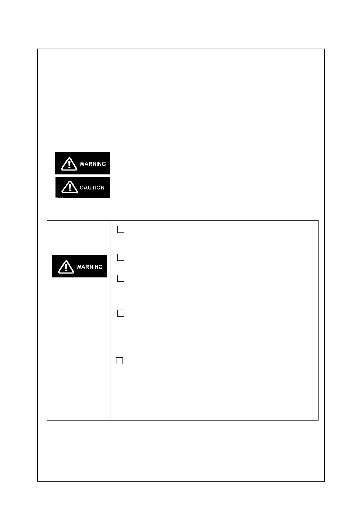
Manual classifies the safety caution level into "WARNING" and "CAUTION" using alert symbols
as follows.
Failure to observe the instructions given in this Manual could result
in death or bodily injury of the operator.
Failure to observe the instructions given in this Manual could result in
risk of bodily injury or physical damage to equipment, etc.
Don't overhaul the module and don't touch the module internals,
with the power switch kept ON.
Failure to observe this instruction could result in electric shock.
Don't touch the terminals with the power switch kept ON.
Failure to observe this instruction could result in electric shock.
Execute write during PC run (write during run) only when cyclic
operation of main equipment/machine is in shutdown.
Failure to observe this instruction could result in breakdown of its
device(s) and bodily injury from mis-operation, if any.
In handling the lithium battery, read and observe " Lithium Battery
Handling Cautions " given in this Manual. Improper handling
would cause liquid leak, overheat, sparking, and fracture, which
could then result in breakdown of units and devices and bodily
injury.
Regarding safe-related signals and emergency stop circuit, etc.,
handle those signals in external units without through this system.
ii
Page 5

Use this product under an environment which meets the
environmental general specification specified in this Manual.
Don't attach/detach each module to/from its base, with the power
switch kept ON.
Don't touch directly the electronic circuits inside the module.
Failure to observe this instruction could result in breakdown of the
module by static electricity.
iii
Page 6
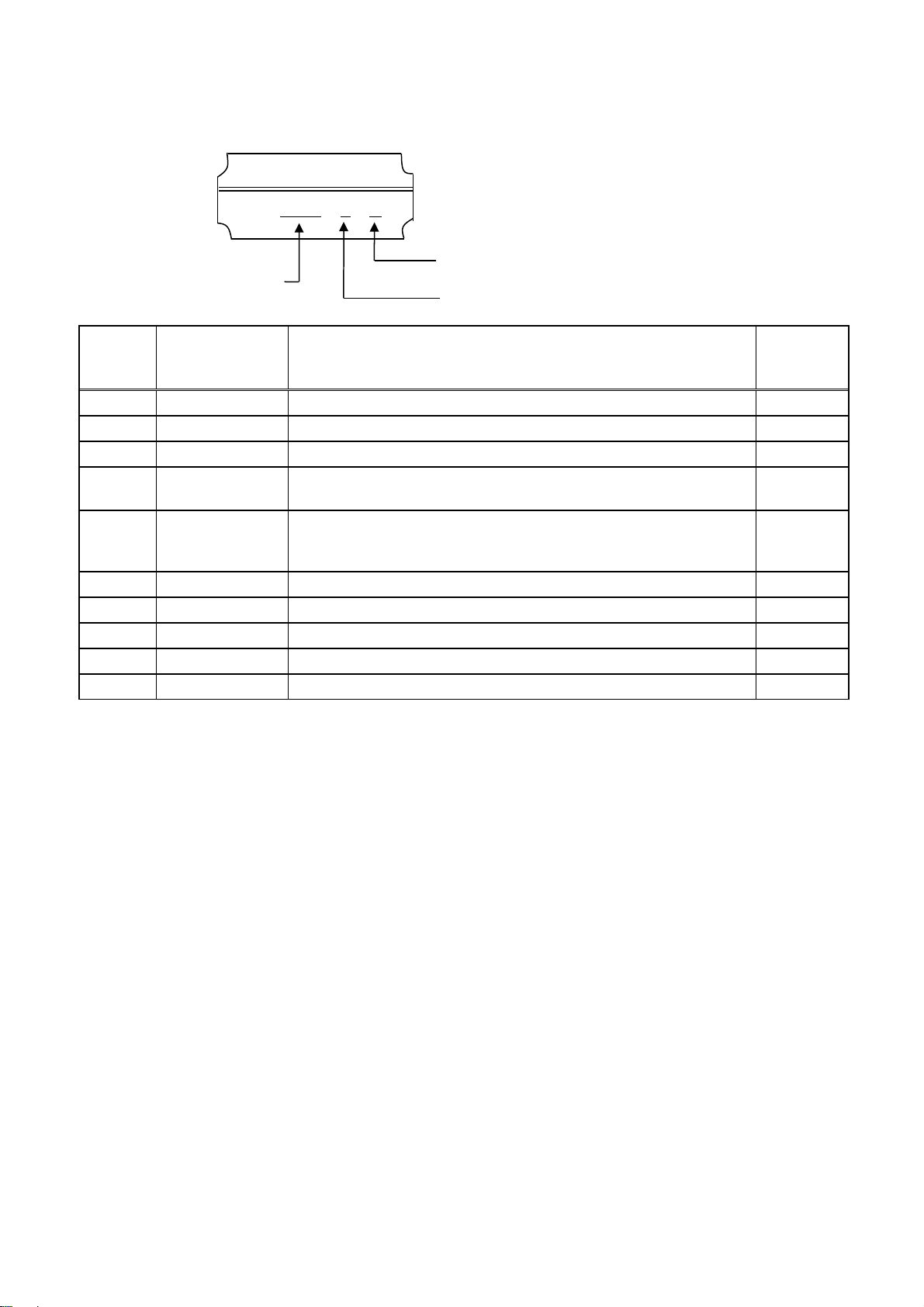
REVISION HISTORY OF OPERATION MANUAL
g
j
T
Operation manual revision No. is added as a part of Manual No. described on the cover sheet of
the manual.
Operation Manual No.
T - 3 0 7 # E
N: Japanese E: English
Series No.
Revision symbol
Revision
No.
1 2003.06.30 1st revision
2 2004.09.02 Correction of MSET/CSET command
3 2005.01.10 Correction of CSET command
4 2006.01.01
5 2006.03.20
6 2006.11.10 Correct missing description.
7 2007.03.30 Correction of I/O address allocation
8 2012.05 TOYODA brand logo added on the front cover
9 2013.04 Correction of errors
10 2022.03 TOYODA brand logo removed
Date of Revision Revision Details
The company name “TOYODA MACHINE WORKS,LTD”
is chan
ed to “JTEKT CORPORATION”
Special register was corrected.
The device that was able to use the PC3 series was corrected.
Clock ad
ustment instruction is added
Equivalent
Japanese
manual
version
-3079N
iv
Page 7

Composition of Related Operation Manuals
Operation
manual No.
T-822#E PC2 series
T-833#E PC2J series
T-845#E PC2J SUB-CPU
T-862#E PC2JN
T-873#E
T-880#E PC2S1 series
T-300#E PC3J series
T-303#E PC3JNF/PC3JNM
T-304#E PC3JM
T-310#E PC3JD
T-320#E PC3JB series
T-311#E PC3JG
PC2JNM
PC2JNF
Title Outline
This manual describes the basic
operating procedure, functions, and
specifications of PC2 series.
This manual describes the basic
operating procedure, functions, and
specifications of PC2J series.
This manual describes the basic operating
procedure, functions, and specifications of
SUB-CPU.
This manual describes the basic operating
procedure, functions, and specifications of
PC2JN.
This manual describes the basic operating
procedure, functions, and specifications of
PC2JNM/PC2JNF.
This manual describes the basic operating
procedure, functions, and specifications of
PC2S1 series.
This manual describes the basic operating
procedure, functions, and specifications of
PC3J series.
This manual describes the basic operating
procedure, functions, and specifications of
PC3JNF/PC3JNM.
This manual describes the basic operating
procedure, functions, and specifications of
PC3JM.
This manual describes the basic operating
procedure, functions, and specifications of
PC3JD.
This manual describes the basic operating
procedure, functions, and specifications of
PC3JB series.
This manual describes the basic operating
procedure, functions, and specifications of
PC3JG.
v
Page 8
This manual describes programming with the TOYOPUC-PC2/3 series.
Although the basic programming method is common to all the PC2/3 series, there are differences
in the application instructions and the external I/O devices which can be used and in the program
capacities, etc. Model-specific functions are marked as shown below. Common functions are not
marked.
Along with this manual, it is recommended that you read the operation manuals for TOUOPUC.
PC/L2-specific functions------------------PC2/L2
PC2J series-specific function------------PC2J
The PC2J series controllers are classified into two types according to the program capacity.
8KW
PC2J
PC2JS
PC2JR
PC2JF
PC2F
PC2FS
PC2J-8KW
16KW
PC2JC
PC2J16
SUB-CPU
PC2JN
PC2J-16KW
32KW
PC2JNM
PC2JNF
PC2J-32KW
PC3J-specific functions---------------PC3J
PC3JG-specific functions-------------PC3JG
Ver.---------This is usable for the specific version or later.
PC2/L2, PC2J : Ver 3.50 or later
PC2JS/JR : Ver2.30 or later
PC2JC : Ver 3.20 or later
PC2J16 : Ver2.10 or later
SUB-CPU : Ver2.50 or later
PC2JNM/PC2JNF : Ver2.00 or later
This is not usable for PC2JN.
vi
Page 9

Contents
FOREWORD
FOR SAFETY OPERATION
REVISION HISTORY OF OPERATION MANUAL
Composition of Related Operation Manuals
Contents 1
1. MAKINK SEQUENCE CIRCUITS.........................................................................................................................1-1
1.1. Usage of TOYOPUC...................................................................................................................................... 1-1
1.1.1. Connection between I/O devices and TOYOPUC...................................................................................1-1
1.1.2. I/O address.............................................................................................................................................. 1-1
1.2. Circuit diagram configuration ......................................................................................................................... 1-4
1.3. I/O circuit ........................................................................................................................................................ 1-5
1.3.1. Input section ............................................................................................................................................1-5
1.3.2. Output section..........................................................................................................................................1-6
1.4. Logic section ..................................................................................................................................................1-7
1.4.1. Internal relay (dummy output).................................................................................................................. 1-7
1.4.2. Timer........................................................................................................................................................ 1-8
1.4.3. Counter....................................................................................................................................................1-9
1.4.4. Keep relay..............................................................................................................................................1-10
1.4.5. Edge detection....................................................................................................................................... 1-11
1.4.6. Special relay..........................................................................................................................................1-12
1.4.7 Link relay ................................................................................................................................................1-37
1.4.8. Designation of Register Bit PC3J........................................................................................................ 1-38
1.5. Application instruction...................................................................................................................................1-39
1.5.1. Application instruction............................................................................................................................ 1-39
1.5.2. Data register.......................................................................................................................................... 1-39
1.5.3. File register............................................................................................................................................ 1-40
1.5.4. Link register........................................................................................................................................... 1-40
1.5.5. Current value register............................................................................................................................1-40
1.5.6. Buffer register PC3JG............................................................................................................................1-40
1.5.7. Special register...................................................................................................................................... 1-41
2. EXECUTION OF PROGRAM............................................................................................................................... 2-1
2.1. Processing operation......................................................................................................................................2-1
2.2. Subroutine......................................................................................................................................................2-4
2.3. Interrupt program PC2/L2............................................................................................................................ 2-5
2.3.1. Periodic interrupt......................................................................................................................................2-5
2.3.2. External interrupt .....................................................................................................................................2-6
2.3.3. Interrupt program considerations.............................................................................................................2-7
2.4. Scan time ....................................................................................................................................................... 2-8
3. PARAMETER........................................................................................................................................................ 3-1
3.1. Contents of parameters.................................................................................................................................. 3-1
3.2. Setting the parameters................................................................................................................................... 3-4
3.2.1. Auto setting by CPU module....................................................................................................................3-4
3.2.1.1. In case of PC2/L2, PC2J.............................................................................................................. 3-4
3.2.1.2. In case of PC3J series.................................................................................................................3-8
3.2.2. Setting with a peripheral device...............................................................................................................3-9
4. USER MEMORY STRUCTURE............................................................................................................................4-1
4.1. Program memory structure ............................................................................................................................ 4-1
4.1.1. In case of PC2/L, PC2J ........................................................................................................................... 4-1
4.1.2. In case of PC3J series............................................................................................................................. 4-2
4.2. Data memory structure................................................................................................................................. 4-11
4.2.1. In case of PC2/L, PC2J ......................................................................................................................... 4-1 1
4.2.1.1. Data memory map........................................................................................................................... 4-11
4.2.1.2. Data memory address..................................................................................................................... 4-12
4.2.2. In case of PC3J series........................................................................................................................... 4-15
4.2.2.1. Data memory map...........................................................................................................................4-15
4.2.2.2. I/O address table ........................................................................................................................4-18
5. INSTRUCTION WORDS.......................................................................................................................................5-1
5.1. Basic instructions ...........................................................................................................................................5-1
Page 10

5.1.1. Extension on the PC3J series .................................................................................................................5-2
1.STR, STR NOT............................................................................................................................................5-6
2.AND, AND NOT...........................................................................................................................................5-7
3.OR, OR NOT ...............................................................................................................................................5-8
4.AND STR.....................................................................................................................................................5-9
5.OR STR..................................................................................................................................................... 5-10
6.
...
OUT....................................................................................................................................................... 5-11
7.
....
SET.......................................................................................................................................................5-12
8.
...
RST.......................................................................................................................................................5-13
9.PTS, NTS...................................................................................................................................................5-14
10.FPS, FRD, FPP .......................................................................................................................................5-16
11.
...
FST.......................................................................................................................................................5-17
12..NOT.......................................................................................................................................................5-18
13..NOP.......................................................................................................................................................5-19
5.2. Timer and counter instructions..................................................................................................................... 5-20
1.TMRH (Direct mode 10ms timer) .......................................................................................................... 5-25
2.TMRH (Indirect mode 10ms timer)........................................................................................................5-26
3.TMR (Direct mode 100ms timer)...........................................................................................................5-27
4.TMR (Indirect mode 100ms timer) ........................................................................................................5-28
5.TMRSH (Direct mode 10ms integrating timer)...................................................................................... 5-29
6.TMRSH (Indirect mode 10ms integrating timer) ................................................................................... 5-30
7.TMRS (Direct mode 100 ms integrating timer) .....................................................................................5-31
8.TMRS (Indirect mode 100 ms integrating timer)...................................................................................5-32
9.CNT (Direct mode up counter)..............................................................................................................5-33
10.CNT (Indirect mode up counter).......................................................................................................... 5-34
11.CNTD (Direct mode down counter).....................................................................................................5-35
12.CNTD (Indirect mode down counter) ..................................................................................................5-36
13.CNTH (Direct mode up/down counter)................................................................................................5-37
14.CNTH (Indirect up/down counter) .......................................................................................................5-39
15.ETMRH Extended 10ms Timer...........................................................................................................5-41
16.ETMR Extended 100ms Timer............................................................................................................ 5-42
17.ETMRSH Extended 10ms Integrating Timer....................................................................................... 5-43
18.ETMRS Extended 100ms Integrating Timer .......................................................................................5-44
19.ECNT Extended Counter (UP)............................................................................................................ 5-45
20.ECNTD Extended Counter (Down).....................................................................................................5-46
21.ECNTH Extended Counter (Up-Down) ............................................................................................... 5-47
5.3. Contact type application instructions............................................................................................................5-48
1.=H 2-digit hexadecimal constant comparison (=)..................................................................................5-50
2.=D 3-digit decimal constant comparison (=)..........................................................................................5-51
3.=N Byte data comparison (=) ................................................................................................................5-52
4.W=H 4-digit hexadecimal constant comparison (=).............................................................................. 5-53
5.W=D 5-digit decimal constant comparison (=)......................................................................................5-54
6.W=N Word data comparison (=)............................................................................................................5-55
7.D=H 8-digit hexadecimal constant comparison (=) *.............................................................................5-56
8.D=D 10-digit decimal constant comparison (=) * ..................................................................................5-57
9.D=N 32-bit data comparison (=) * ......................................................................................................... 5-58
10.<>H 2-digit hexadecimal constant comparison (<>)...........................................................................5-59
11.<>D 3-digit decimal constant comparison (<>)....................................................................................5-60
12.<>N Byte data comparison (<>)..........................................................................................................5-61
13.W<>H 4-digit hexadecimal constant comparison (<>)........................................................................ 5-62
14.W<>D 5-digit decimal constant comparison (<>)................................................................................5-63
15.W<>N Word data comparison (<>)..................................................................................................... 5-64
16.D<>H 8-digit hexadecimal constant comparison (<>) * ...................................................................... 5-65
17.D<>D 10-digit decimal constant comparison (<>) *............................................................................5-66
18.D<>N 32-bit data comparison (<>) * ...................................................................................................5-67
19.>H 2-digithexadecimal constant comparison (>)................................................................................. 5-68
20.>D 3-digit decimal constant comparison (>)........................................................................................5-69
21.>N Byte data comparison (>) .............................................................................................................. 5-70
22.W>H 4-digit hexadecimal constant comparison (>)............................................................................5-71
23.W>D 5-digit decimal constant comparison (>).................................................................................... 5-72
Page 11

24.W>N Word data comparison (>)..........................................................................................................5-73
25.D>H 8-digit hexadecimal constant comparison (>) *........................................................................... 5-74
26.D>D 10-digit decimal constant comparison (>) * ................................................................................5-75
27.D>N 32-bit data comparison (>) * ....................................................................................................... 5-76
28.>=H 2-digit hexadecimal constant comparison (>=)...........................................................................5-77
29.>=D 3-digit decimal constant comparison (>=)................................................................................... 5-78
30.>=N Byte data comparison (>=)..........................................................................................................5-79
31.W>=H 4-digit hexadecimal constant comparison (>=)........................................................................ 5-80
32.W>=D 5-digit decimal constant comparison (>=)................................................................................5-81
33.W>=N Word data comparison (>=)..................................................................................................... 5-82
34.D>=H 8-digit hexadecimal constant comparison (>=) * ...................................................................... 5-83
35.D>=D 10-digit decimal constant comparison (>=) *............................................................................5-84
36.D>=N 32-bit data comparison (>=) * ...................................................................................................5-85
37.<H 2-digit hexadecimal constant comparison (<)................................................................................5-86
38.<D 3-digit decimal constant comparison (<)........................................................................................5-87
39.<N Byte data comparison (<) *............................................................................................................ 5-88
40.W<H 4-digit hexadecimal constant comparison (<)............................................................................5-89
41.W<D 5-digit decimal constant comparison (<).................................................................................... 5-90
42.W<N Word data comparison (<) *.......................................................................................................5-91
43.D<H 8-digit hexadecimal constant comparison (<) *........................................................................... 5-92
44.D<D 10-digit decimal constant comparison (<) * ................................................................................5-93
45.D<N 32-bit data comparison (<) * ....................................................................................................... 5-94
46.<=H 2-digit hexadecimal constant comparison (<=)...........................................................................5-95
47.<=D 3-digit decimal constant comparison (<=)................................................................................... 5-96
48.<=N Byte data comparison (<=) *........................................................................................................5-97
49.W<=H 4-digit hexadecimal constant comparison (<=)........................................................................ 5-98
50.W<=D 5-digit decimal constant comparison (<=)................................................................................5-99
51.W<=N Word data comparison (<=) *................................................................................................. 5-100
52.D<=H 8-digit hexadecimal constant comparison (<=) * .................................................................... 5-101
53.D<=D 10-digit decimal constant comparison (<=) *..........................................................................5-102
54.D<=N 32-bit data comparison (<=) * .................................................................................................5-103
5.4. Output type application instructions Note)............................................................................................... 5-104
5.4.1. Transfer instructions ............................................................................................................................ 5-122
1.MOV 2-digit Hex constant transfer (FUN100).....................................................................................5-123
2.WMOV 4-digit Hex constant transfer (FUN101).................................................................................. 5-124
3.DMOV 8-digit Hex constant transfer (FUN102) ..................................................................................5-125
4.MOVP 2-digit BCD constant transfer (FUN103)..................................................................................5-126
5.WMOVP 4-digit BCD constant transfer (FUN1)..................................................................................5-127
6.DMOVP 8-digit BCD constant transfer (FUN104)...............................................................................5-128
7.MOVR 3-digit decimal constant transfer (FUN105) ............................................................................ 5-129
8.WMOVR 5-digit decimal constant transfer (FUN7)............................................................................. 5-130
9.DMOVR 10-digit decimal constant transfer (FUN106)........................................................................ 5-131
10.MOVQ 3-digit octal transfer (FUN107)..............................................................................................5-132
11.WMOVQ 6-digit octal transfer (FUN8)...............................................................................................5-133
12.DMOVQ 11-digit octal transfer (FUN108) .........................................................................................5-134
13.MOVT 2-digit Hex constant transfer to two places (FUN62).............................................................5-135
14.WMOVT 4-digit Hex constant transfer to two places (FUN 110).......................................................5-136
15.MOVE 1-byte data direct transfer (FUN90).......................................................................................5-137
16.WMOVE 2-byte data direct transfer (FUN0) .....................................................................................5-138
17.DMOVE 4-byte data direct transfer (FUN111)...................................................................................5-139
18.MOVF 1-byte data indirect transfer 1 (FUN74).................................................................................5-140
19.WMOVF 2-byte data indirect transfer 1 (FUN112)............................................................................5-141
20.DMOVF 4-byte data indirect transfer 1 (FUN113) *..........................................................................5-142
21.MOVG 1-byte data indirect transfer 2 (FUN75) ................................................................................5-143
22.WMOVG 2-byte data indirect transfer 2 (FUN114)........................................................................... 5-144
23.DMOVG 4-byte data indirect transfer 2 (FUN115) *..........................................................................5-145
24.MOVH 1-byte data indirect transfer 3 (FUN76).................................................................................5-146
25.WMOVH 2-byte data indirect transfer 3 (FUN116) ...........................................................................5-147
26.DMOVH 4-byte data indirect transfer 3 (FUN117) *.......................................................................... 5-148
27.BMOV1 Byte data block transfer 1 (FUN70).....................................................................................5-149
Page 12

28.BMOV2 Byte data block transfer 2 (FUN118) *.................................................................................5-150
29.WBMOV Word data block transfer (FUN119) *.................................................................................5-151
30.BMVI Byte data indirect block transfer (FUN71)...............................................................................5-152
31.WBMVI Word data indirect block transfer (FUN120) *......................................................................5-153
32.DIV Byte data delivery (FUN5)..........................................................................................................5-154
33.WDIV Word data delivery (FUN122).................................................................................................5-155
34.DDIV 32-bit data delivery (FUN123) *...............................................................................................5-156
35.BDIV Byte data block delivery(FUN72).............................................................................................5-157
36.WBDIV Word data block delivery(FUN126) ......................................................................................5-158
37.PUP Byte data extraction (FUN6) .....................................................................................................5-159
38.WPUP Word data extraction (FUN124) ............................................................................................5-160
39.DPUP 32-bit data extraction (FUN125) * ..........................................................................................5-161
40.BPUP Byte data block extraction(FUN73) ........................................................................................ 5-162
41.WBPUP Word data block extraction(FUN127).................................................................................. 5-163
42.SXCH 4-bit data exchange(FUN53)..................................................................................................5-164
43.XCH 8-bit data exchange(FUNl32) ................................................................................................... 5-165
44.WXCH 16-bit data exchange(FUN2)................................................................................................. 5-166
45.DXCH 32-bit data exchange(FUN133) *...........................................................................................5-167
46.BXCH Byte data block exchange(FUN134)......................................................................................5-168
47.WBXCH Word data block exchange (FUN 135) ...............................................................................5-169
48.JIS Storage in JIS code (FUN 109)...................................................................................................5-170
49.FIL1 Byte data fill 1 (FUN 77)............................................................................................................5-171
50.FIL2 Byte data fill 2 (FUN 128) * .......................................................................................................5-172
51.WFIL Word data fill (FUN 129) *........................................................................................................5-173
52.FILI1 Byte data indirect fill 1 (FUN 78)..............................................................................................5-174
53.FILI2 Byte data indirect fill 2 (FUN 130) * .........................................................................................5-175
54.WFILI Word data indirect fill (FUN 131) *..........................................................................................5-176
55.CMOV Byte data transfer on clearance confirmation (FUN 20)........................................................5-177
56.WCMOV Word data transfer on clearance confirmation (FUN 166)................................................. 5-178
57.CLR Matching data clearance (byte) (FUN 21).................................................................................5-179
58.WCLR Matching data clearance (Word) (FUN 167) ......................................................................... 5-180
59.REF External input transfer (FUN 283) !#..........................................................................................5-181
60.REFO External output transfer (FUN 284) !#.....................................................................................5-182
61.MOVJ 1-byte transfer from register to file register (FUN 144) %&.....................................................5-183
62.WMOVJ 2-byte transfer from register to file register (FUN 145) %&..................................................5-184
63.DMOVJ 4-byte transfer from register to file register (FUN 146) %&...................................................5-185
64.MOVK 1-byte transfer from file register to register (FUN 147) %&.....................................................5-186
65.WMOVK 2-byte transfer from file register to register (FUN 148) %&.................................................5-187
66.DMOVK 4-byte transfer from file register to register (FUN 149) %&..................................................5-188
5.4.2. Arithmetic operations...........................................................................................................................5-189
67.+ Byte data binary addition (FUN 168).............................................................................................. 5-190
68.W+ Word data binary addition (FUN 92)........................................................................................... 5-191
69.D+ 32-bit data binary addition (FUN 169) .........................................................................................5-192
70.+P 2-digit BCD addition (FUN 177)................................................................................................... 5-193
71.W+P 4-digit BCD addition (FUN 10) ................................................................................................. 5-194
72.D+P 8-digit BCD addition (FUN 178) ................................................................................................5-195
73.- Byte data binary subtraction (FUN 170) .........................................................................................5-196
74.W- Word data binary subtraction (FUN 93).......................................................................................5-197
75.D- 32-bit data binary subtraction (FUN 171).....................................................................................5-198
76.-P 2-digit BCD subtraction (FUN 179)...............................................................................................5-199
77.W-P 4-digit BCD subtraction (FUN 11)..............................................................................................5-200
78.D-P 8-digit BCD subtraction (FUN 180)............................................................................................ 5-201
79.* Byte data binary multiplication (FUN 172)...................................................................................... 5-202
80.W* Word data binary multiplication (FUN 94) ................................................................................... 5-203
81.D* 32-bit data binary multiplication (FUN 173)..................................................................................5-204
82.*P 2-digit BCD multiplication (FUN 181) ...........................................................................................5-205
83.W*P 4-digit BCD multiplication (FUN 182)........................................................................................5-206
84.D*P 8-digit BCD multiplication (FUN 183).........................................................................................5-207
85.W/B Word data binary division 1 (FUN 95) ....................................................................................... 5-208
86./ Byte data binary division (FUN 174) #.............................................................................................5-209
Page 13

87.W/ Word data binary division 2 (FUN 175) #.....................................................................................5-210
88.D/ 32-bit data binary division (FUN 176) #......................................................................................... 5-211
89./P 2-digit BCD division (FUN 184).....................................................................................................5-212
90.W/P 4-digit BCD division (FUN 185) ................................................................................................. 5-213
91.D/P 8-digit BCD division (FUN 186)..................................................................................................5-214
5.4.3 Logical operation instructions...............................................................................................................5-215
92.AND Byte data logical product(AND) (FUN 13)................................................................................5-216
93.WAND Word data logical product(AND) (FUN 187).......................................................................... 5-217
94.DAND 32-bit data logical product(AND) (FUN 188).......................................................................... 5-218
95.OR Byte data logical sum(OR) (FUN 14)..........................................................................................5-219
96.WOR Word data logical sum(OR) (FUN 189)................................................................................... 5-220
97.DOR 32-bit data logical sum(OR) (FUN 190) ...................................................................................5-221
98.NOT Byte data inversion (FUN 9) .....................................................................................................5-222
99.WNOT Word data inversion (FUN 191) ............................................................................................5-223
100.DNOT 32-bit data inversion (FUN 192)...........................................................................................5-224
101.XOR Byte data exclusive logical sum(XOR) (FUN 18) ................................................................... 5-225
102.WXOR Word data exclusive logical sum(XOR) (FUN 193) ............................................................ 5-226
103.DXOR 32-bit data exclusive logical sum(XOR) (FUN 194).............................................................5-227
5.4.4 Increment and decrement....................................................................................................................5-228
104.INC Byte data binary increment (FUN 195) ....................................................................................5-229
105.WINC Word data binary increment (FUN 63)..................................................................................5-230
106.DINC 32-bit data binary increment (FUN 196)................................................................................ 5-231
107.INCP 2-digit BCD increment (FUN 199)..........................................................................................5-232
108.WINCP 4-digit BCD increment (FUN 200)......................................................................................5-233
109.DINCP 8-digit BCD increment (FUN 201).......................................................................................5-234
110.DEC Byte data binary decrement (FUN 197)..................................................................................5-235
111.WDEC Word data binary decrement (FUN 64) ............................................................................... 5-236
112.DDEC 32-bit data binary decrement (FUN 198) .............................................................................5-237
113.DECP 2-digit BCD decrement (FUN 202).......................................................................................5-238
114.WDECP 4-digit BCD decrement (FUN 203)....................................................................................5-239
115.DDECP 8-digit BCD decrement (FUN 204).....................................................................................5-240
5.4.5. Search .................................................................................................................................................5-241
116.SRH1 Byte data search 1 (FUN 88)................................................................................................5-242
117.WSRH1 Word data search 1 (FUN 89)........................................................................................... 5-244
118.SRH2 Byte data search 2 (FUN 212)..............................................................................................5-246
119.WSRH2 Word data search 2 (FUN 213).........................................................................................5-248
120.DSRH 32-bit data Search (FUN 214)..............................................................................................5-250
5.4.6 Parity....................................................................................................................................................5-252
121.MKP1 Odd parity composition (FUN 83).........................................................................................5-253
122.MKP2 Even parity composition (FUN 81) .......................................................................................5-254
123.PCH1 Odd parity check (FUN 84)...................................................................................................5-255
124.PCH2 Even Parity check (FUN 82)................................................................................................. 5-256
5.4.7. Data conversion...................................................................................................................................5-257
125.BIN 2-digit BCD to 8-bit binary (FUN 152)...................................................................................... 5-258
126.WBIN 4-digit BCD to 16-bit binary (FUN 3).....................................................................................5-259
127.DBIN 8-bit BCD to 32-bit binary (FUN 153)....................................................................................5-260
128.BCD 8-bit binary to 2-digit BCD (FUN 154) .................................................................................... 5-261
129.WBCD 16-bit binary to 4-bit BCD (FUN 4)......................................................................................5-262
130.DBCD 32-bit binary to 8-digit BCD (FUN 155)................................................................................ 5-263
131.JBIN JIS code to binary (FUN 156).................................................................................................5-264
132.BJIS Binary to JIS code (FUN 157) ................................................................................................5-266
133.DECO 4 to 16 decoder (FUN 50)....................................................................................................5-268
134.ENCO 16 to 4 encoder (FUN 51)....................................................................................................5-270
135.SEG 7-segment decode (FUN 52).................................................................................................. 5-272
136.WTIM1 Hours, minutes, and seconds to seconds (FUN 158) ........................................................5-274
137.WTIM2 Seconds to hours, minutes and seconds (FUN 159) ......................................................... 5-276
138.CDSET Code conversion set (FUN 85).......................................................................................... 5-278
139.CDO1 Code conversion output 1 (FUN 86) ....................................................................................5-279
140.CDO2 Code conversion output 2 (FUN 87) ....................................................................................5-280
Page 14

5.4.8 Comparison..........................................................................................................................................5-281
141.CP Byte data comparison (FUN 17)................................................................................................5-282
142.WCP Word data comparison (FUN 12)...........................................................................................5-283
143.DCP 32-bit data comparison (FUN 211) .........................................................................................5-284
5.4.9. Bit operation.........................................................................................................................................5-285
144.BSET Byte data bit set (FUN 136) *................................................................................................ 5-286
145.WBSET Word data set (FUN 137).................................................................................................. 5-287
146.DBSET 32-bit data bit set (FUN 138) * ...........................................................................................5-288
147.BRST Byte data bit reset (FUN 139) * ............................................................................................ 5-289
148.WBRST Word data bit reset (FUN 140)..........................................................................................5-290
149.DBRST 32-bit data bit reset (FUN 141) *........................................................................................ 5-291
150.BPU Bit extraction (FUN 54) *.........................................................................................................5-292
151.WBPU Word data bit extraction (FUN 142).....................................................................................5-293
152.DBPU 32-bit data extraction (FUN 143) * .......................................................................................5-294
153.SUM Byte data ON-bit count (FUN 208).........................................................................................5-295
154.WSUM Word data ON-bit count (FUN 209).................................................................................... 5-296
155.DSUM 32-bit data ON-bit count (FUN 210) .................................................................................... 5-297
5.4.10 Shift....................................................................................................................................................5-298
156.SFR Byte data 1 bit right shift (FUN 217) *.....................................................................................5-299
157.WSFR Word data 1 bit right shift (FUN 36) *..................................................................................5-300
158.DSFR 32-bit data 1 bit right shift (FUN 218) *.................................................................................5-301
159.BSFR Byte data n bits right shift (FUN 224) *.................................................................................5-302
160.WBSFR Word data n bits right shift (FUN 225) *............................................................................5-303
161.DBSFR 32-bit data n bits right shift (FUN 226) *.............................................................................5-304
162.SFL Byte data 1 bit left shift (FUN 219) *........................................................................................5-305
163.WSFL Word data 1 bit left shift (FUN 37) * .....................................................................................5-306
164.DSFL 32-bit data 1 bit left shift (FUN 220) *....................................................................................5-307
165.BSFL Byte data n bits left shift (FUN 227) *....................................................................................5-308
166.WBSFL Word data n bits left shift (FUN 228) *...............................................................................5-309
167.DBSFL 32-bit data n bits left shift (FUN 229) *................................................................................5-310
168.SRL Byte data 1 bit right-left shift (FUN 221) * ............................................................................... 5-311
169.WSRL Word data 1 bit right-left shift (FUN 222) *...........................................................................5-312
170.DSRL 32-bit data 1 bit right-left shift (FUN 223) *...........................................................................5-313
171.BSRL Byte data n bits right-left shift (FUN 230)..............................................................................5-314
172.WBSRL Word data n bits right-left shift (FUN 231).........................................................................5-315
173.DBSRL 32-bit data n bits right-left shift (FUN 232) ......................................................................... 5-316
174.SUP 4 bit data upper-digit direction shift (FUN 251)....................................................................... 5-317
175.UP1 Byte data upper-digit direction shift 1 (FUN 91)......................................................................5-318
176.UP2 Byte data upper-digit direction shift 2 (FUN 252).................................................................... 5-319
177.WUP Word data upper-digit direction shift (FUN 253).................................................................... 5-320
178.DUP 32-bit data upper-digit direction shift (FUN 254) ....................................................................5-321
179.SDOWN 4 bit data lower-digit direction shift (FUN 255)................................................................. 5-323
180.DOWN Byte data lower-digit direction shift (FUN 256)...................................................................5-324
181.WDOWN Word data lower-digit direction shift (FUN 257) .............................................................. 5-325
182.DDOWN 32-bit data lower-digit direction shift (FUN 258)...............................................................5-326
183.FIFW Byte data FIFO write (FUN 160)............................................................................................ 5-328
184.WFIFW Word data FIFO write (FUN 161).......................................................................................5-329
185.DFIFW 32-bit data FIFO write (FUN 162).......................................................................................5-330
186.FIFR Byte data FIFO read (FUN 163).............................................................................................5-332
187.WFIFR Word data FIFO read (FUN 164)........................................................................................ 5-334
188.DFIFR 32-bit data FIFO read (FUN 165) ........................................................................................5-336
189.SFIN Accumulation shift input (FUN 68).........................................................................................5-338
190.SFOUT Accumulation shift output (FUN 69)...................................................................................5-340
5.4.11. Rotate.................................................................................................................................................5-342
191.RRC Byte data right rotate with carry (FUN 233) * .........................................................................5-343
192.WRRC Word data right rotate with carry (FUN 234) * ....................................................................5-344
193.DRRC 32-bit data right rotate with carry (FUN 235) *..................................................................... 5-345
194.RR Byte data right rotate without carry (FUN 242) *.......................................................................5-346
195.WRR Word data right rotate without carry (FUN 243) *.................................................................. 5-347
196.DRR 32-bit data right rotate without carry (FUN 244) *.................................................................. 5-348
Page 15

197.RLC Byte data left rotate with carry (FUN 236) *............................................................................ 5-349
198.WRLC Word data left rotate with carry (FUN 237) * .......................................................................5-350
199.DRLC 32-bit data left rotate with carry (FUN 238) *........................................................................5-351
200.RL Byte data left rotate without carry (FUN 245) *.......................................................................... 5-352
201.WRL Word data left rotate without carry (FUN 246) *.....................................................................5-353
202.DRL 32-bit data left rotate without carry (FUN 247) * .....................................................................5-354
203.RLRC Byte data right-left rotate with carry (FUN 239).................................................................... 5-355
204.WRLRC Word data right-left rotate with carry (FUN 240)............................................................... 5-356
205.DRLRC 32-bit data right-left rotate with carry (FUN 241)............................................................... 5-357
206.RLR Byte data right-left rotate without carry (FUN 248) .................................................................5-358
207.WRLR Word data right-left rotate without carry (FUN 249) ............................................................ 5-359
208.DRLR 32-bit data right-left rotate without carry (FUN 250)............................................................. 5-360
5.4.12. Programmed branch.......................................................................................................................... 5-361
209.JMP JUMP (FUN 272).....................................................................................................................5-362
210.CALL Subroutine call (FUN 273).....................................................................................................5-363
211.RET Return from subroutine (FUN 464)..........................................................................................5-364
212.FOR Start repetition (FUN 472) #....................................................................................................5-365
213.FORN Start repetition (indirect) (FUN 476) #...................................................................................5-366
214.NEXT End of repetition (FUN 480) #...............................................................................................5-367
5.4.13 Master control ....................................................................................................................................5-368
215.MC Master control set (FUN 440)...................................................................................................5-369
216.MCR Master control reset (FUN 444) .............................................................................................5-370
5.4.14. Input/output control............................................................................................................................5-371
217.RIO Input/output refresh (FUN 280) !..............................................................................................5-372
218.RI Input refresh (FUN 281)..............................................................................................................5-373
219.RO Output refresh (FUN 282)......................................................................................................... 5-374
5.4.15. Sequential interrupt ........................................................................................................................... 5-375
220.DI Interrupt inhibit (FUN 276) %.......................................................................................................5-376
221.PDI Partial interrupt inhibit (FUN 278) %.........................................................................................5-377
222.EI Interrupt enable (FUN 277) %......................................................................................................5-378
223.PEI Partial interrupt enable (FUN 279) %........................................................................................5-379
224.RETI Return from interrupt routine (FUN 468) %.............................................................................5-380
5.4.16. Label.................................................................................................................................................. 5-381
225.START Main program start (FUN 448)............................................................................................5-382
226.END Main program end (FUN 452).................................................................................................5-383
227.PEND End of program (FUN 456)................................................................................................... 5-384
228.LABEL Label (FUN 460)..................................................................................................................5-385
5.4.17 Special module data transfer .............................................................................................................5-386
229.SPR Special module byte-data readout (for readout of file for the SIO module) (FUN 304)........5-387
230.SPW Special module byte-data write (for writing of file for the SIO module) (FUN 306)............. 5-389
231.HCR High-speed counter data readout (FUN 316) !.......................................................................5-391
232.HCW High-speed counter data write (FUN 317) !...........................................................................5-392
233.IOR Shared I/O unit data readout (for A/D module) (FUN 318) !....................................................5-393
234.IOW Shared I/O unit data write (for A/D module) (FUN 319) !........................................................5-394
5.4.18. Sequential debug............................................................................................................................... 5-395
235.ENB Trace enable (FUN 274).........................................................................................................5-396
236.TRG Trace trigger (FUN 275)..........................................................................................................5-397
5.4.19. I/O monitor control.............................................................................................................................5-398
237.KEY I/O monitor key input (FUN 294) %#.........................................................................................5-401
238.LEDD I/O monitor display (FUN 289) %#.........................................................................................5-402
239.LEDC I/O monitor display clear (FUN 290) %#................................................................................5-404
5.4.20. Application instruction for memory card PC2/L2 ............................................................................... 5-405
240.CDR Memory card data read (FUN 296) $......................................................................................5-406
241.CDW Memory card data write (FUN 297) $.....................................................................................5-407
242.CDIR Indirect memory card data read (FUN 298) $........................................................................5-408
243.CDIW Indirect memory card write (FUN 299) $...............................................................................5-409
5.4.21. Other application instruction.............................................................................................................. 5-410
244.SYS Setting/resetting of I/O monitor error automatic indication ..................................................... 5-411
245.ANN Annunciator (FUN 291)...........................................................................................................5-412
246.USC User defined clock (FUN 293)................................................................................................5-413
Page 16

247.ADJ Built-in clock 30-second adjustment (FUN 292) !....................................................................5-414
248.BAUD Peripheral device communication speed setting (FUN 288) #.............................................5-415
249.STOP Program stop (FUN 287)......................................................................................................5-416
250.WDR Scan timer reset (FUN 46).....................................................................................................5-417
5.4.22. Extension of applied instruction for PC3J series PC3J.....................................................................5-418
251.BBMOV Bit Block Transfer (move) (FUN 121) PC3J......................................................................5-422
252.STURN 4bits inversion (FUN 259) PC3J........................................................................................ 5-423
253.TURN 8bits inversion (FUN 260) PC3J...........................................................................................5-423
254.WTURN 16bits inversion (FUN 261) PC3J..................................................................................... 5-423
255.MOVAD Address Constant Transfer (Move) (FUN 320) PC3J.......................................................5-425
256.+H Addition of hexadecimal 2-digit constant (FUN 323) PC3J....................................................... 5-426
257.W+H Addition of hexadecimal 4-digit constant (FUN 324) PC3J....................................................5-427
258.D+H Addition of hexadecimal 8-digit constant (FUN 325) PC3J ....................................................5-428
259.+HP Addition of BCD 2-digit constant (FUN 326) PC3J................................................................. 5-429
260.W+HP Addition of BCD 4-digit constant (FUN 327) PC3J.............................................................. 5-430
261.D+HP Addition of BCD 8-digit constant (FUN 328) PC3J............................................................... 5-431
262.
-H
Deduction of hexadecimal 2-digit constant (FUN 329) PC3J.................................................... 5-432
263.W-H Deduction of hexadecimal 4-digit constant (FUN 330) PC3J................................................. 5-433
264.D-H Deduction of hexadecimal 8-digit constant (FUN 331) PC3J.................................................. 5-434
265.-HP Addition of BCD 2-digit constant (FUN 332) PC3J.................................................................. 5-435
266.W-HP Addition of BCD 4-digit constant (FUN 333) PC3J............................................................... 5-436
267.D-HP Addition of BCD 8-digit constant (FUN 334) PC3J................................................................5-437
268.*H Multiplication of hexadecimal 2-digit constant (FUN 335) PC3J................................................5-438
269.W*H Multiplication of hexadecimal 4-digit constant (FUN 336) PC3J ............................................5-439
270.D*H Multiplication of hexadecimal 8-digit constant (FUN 337) PC3J.............................................5-440
271.*HP Multiplication of BCD 2-digit constant (FUN 338) PC3J .......................................................... 5-441
272.W*HP Multiplication of BCD 4-digit constant (FUN 339) PC3J....................................................... 5-442
273.D*HP Multiplication of BCD 8-digit constant (FUN 340) PC3J........................................................5-443
274./H Divide of hexadecimal 2-digit constant (FUN 341) PC3J........................................................... 5-444
275.W/H Divide of hexadecimal 4-digit constant (FUN 342) PC3J........................................................ 5-445
276.D/H Divide of hexadecimal 8-digit constant (FUN 343) PC3J ........................................................ 5-446
277./HP Divide of BCD 2-digit constant (FUN 344) PC3J .....................................................................5-447
278.W/HP Divide of BCD 4-digit constant (FUN 345) PC3J.................................................................. 5-448
279.D/HP Divide of BCD 8-digit constant (FUN 346) PC3J...................................................................5-449
280.ANDH Logical product (AND) of hexadecimal 2-digit constant (FUN 347) PC3J...........................5-450
281.WANDH Logical product (AND) of hexadecimal 4-digit constant (FUN 348) PC3J........................5-451
282.DANDH Logical product (AND) of hexadecimal 8-digit constant (FUN 349) PC3J ........................5-452
283.ORH Logical sum (OR) of hexadecimal 2-digit constant (FUN 350) PC3J.....................................5-453
284.WORH Logical sum (OR) of hexadecimal 4-digit constant (FUN 351) PC3J.................................5-454
285.DORH Logical sum (OR) of hexadecimal 8-digit constant (FUN 352) PC3J.................................. 5-455
286.XORH Exclusive logical sum (XOR) of hexadecimal 2-digit constant (FUN 353 ) PC3J.................5-456
287.WXORH Exclusive logical sum (XOR) of hexadecimal 4-digit constant (FUN 354) PC3J.............5-457
288.DXORH Exclusive logical sum (XOR) of hexadecimal 8-digit constant (FUN 355) PC3J.............. 5-458
289.STI1 Byte data sum (FUN 362) PC3J............................................................................................. 5-459
290.WSTI1 Word data sum (FUN 363) PC3J........................................................................................5-459
291.DSTI1 32-bit data sum (FUN 364) PC3J.........................................................................................5-459
292.MAX Byte data maximum value retrieve (FUN 374) PC3J.............................................................5-461
293.WMAX Word data maximum value retrieve (FUN 375) PC3J ........................................................ 5-461
294.DMAX 32-bit data maximum value retrieve (FUN 376) PC3J......................................................... 5-461
295.MIN Byte data minimum value retrieve (FUN 377) PC3J ...............................................................5-462
296.WMIN Word data minimum value retrieve (FUN 378) PC3J...........................................................5-462
297.DMIN 32-bit data minimum value retrieve (FUN 379) PC3J........................................................... 5-462
298.AVE Byte data average (FUN 380) PC3J .......................................................................................5-463
299.WAVE Word data average (FUN 381) PC3J...................................................................................5-463
300.DAVE 32-bit data average (FUN 382) PC3J................................................................................... 5-463
301.CRET Return from subroutine (FUN 285) PC3J.............................................................................5-463
302.ARIO Area-designated I/O refresh (FUN 295) PC3J......................................................................5-464
303.SYS Applied command flag clear mode setting (FUN 300) PC3J..................................................5-465
304.BRSET Buffer register(EB) address set (FUN 371) PC3JG.........................................................5-466
305.WBR Data loading from the buffer register(EB) (FUN 372) PC3JG.............................................5-467
Page 17

306.WBW Data saving to the buffer register(EB) (FUN 373) PC3JG .................................................5-468
307.MSET Output of the message for DLNK-M2 (FUN 302) PC3JG .................................................5-469
308.CSET I/O Register read-out instruction issue to TOYOPUC-PCS (FUN 370) PC3JG..................... 5-470
309.SYS Clock adjustment instruction (FUN 300) PC3J.........................................................................5-479
Note) The instructions marked with # can be used by the L2 but not by the PC2 of the version before
SCPU-3.01.
The instructions marked with * can not be use by the PC2 of the some versions.
The available versions are the following as.
CPU Version
PC2J Ver3.50 or later
PC2JS/JR Ver2.30 or later
PC2JF Ver3.50 or later
PC2F Ver4.30 or later
PC2FS Ver2.10 or later
PC2JC Ver3.20 or later
PC2J16 Ver2.10 or later
SUB-CPU Ver2.50 or later
PC2JNM/PC2JNF Ver2.00 or later
PC2JN Ver2.10 or later
The instructions marked with ! can not be used by the SUB-CPU.
The instructions marked with % can be used by the PC2/L2.
The instructions marked with $ can be used by the PC2/L2 of the Ver SCPU-4.10 or later.
The instructions marked with & can be used by the PC3J series.
Page 18

Index of instruction words
- Byte data binary subtraction (FUN 170) 5-196
* Byte data binary multiplication (FUN 172) 5-202
*H Multiplication of hexadecimal 2-digit constant (FUN 335) PC3J 5-438
*HP Multiplication of BCD 2-digit constant (FUN 338) PC3J 5-441
*P 2-digit BCD multiplication (FUN 181) 5-205
/ Byte data binary division (FUN 174) # 5-209
/H Divide of hexadecimal 2-digit constant (FUN 341) PC3J 5-444
/HP Divide of BCD 2-digit constant (FUN 344) PC3J 5-447
/P 2-digit BCD division (FUN 184) 5-212
+ Byte data binary addition (FUN 168) 5-190
+H Addition of hexadecimal 2-digit constant (FUN 323) PC3J 5-426
+HP Addition of BCD 2-digit constant (FUN 326) PC3J 5-429
+P 2-digit BCD addition (FUN 177) 5-193
<=D 3-digit decimal constant comparison (<=) 5-96
<=H 2-digit hexadecimal constant comparison (<=) 5-95
<=N Byte data comparison (<=) * 5-97
<>D 3-digit decimal constant comparison (<>) 5-60
<>H 2-digit hexadecimal constant comparison (<>) 5-59
<>N Byte data comparison (<>) 5-61
<D 3-digit decimal constant comparison (<) 5-87
<H 2-digit hexadecimal constant comparison (<) 5-86
<N Byte data comparison (<) * 5-88
=D 3-digit decimal constant comparison (=) 5-51
=H 2-digit hexadecimal constant comparison (=) 5-50
=N Byte data comparison (=) 5-52
>=D 3-digit decimal constant comparison (>=) 5-78
>=H 2-digit hexadecimal constant comparison (>=) 5-77
>=N Byte data comparison (>=) 5-79
>D 3-digit decimal constant comparison (>) 5-69
>H 2-digithexadecimal constant comparison (>) 5-68
>N Byte data comparison (>) 5-70
ADJ Built-in clock 30-second adjustment (FUN 292) ! 5-414
AND Byte data logical product(AND) (FUN 13) 5-216
AND STR 5-9
AND, AND NOT 5-7
ANDH Logical product (AND) of hexadecimal 2-digit constant (FUN 347) PC3J 5-450
ANN Annunciator (FUN 291) 5-412
ARIO Area-designated I/O refresh (FUN 295) PC3J 5-464
AVE Byte data average (FUN 380) PC3J 5-463
BAUD Peripheral device communication speed setting (FUN 288) # 5-415
BBMOV Bit Block Transfer (move) (FUN 121) PC3J 5-422
BCD 8-bit binary to 2-digit BCD (FUN 154) 5-261
BDIV Byte data block delivery(FUN72) 5-157
BIN 2-digit BCD to 8-bit binary (FUN 152) 5-258
Page 19

BJIS Binary to JIS code (FUN 157) 5-266
BMOV1 Byte data block transfer 1 (FUN70) 5-149
BMOV2 Byte data block transfer 2 (FUN118) * 5-150
BMVI Byte data indirect block transfer (FUN71) 5-152
BPU Bit extraction (FUN 54) * 5-292
BPUP Byte data block extraction(FUN73) 5-162
BRSET Buffer register(EB) address set (FUN 371) PC3JG 5-466
BRST Byte data bit reset (FUN 139) * 5-289
BSET Byte data bit set (FUN 136) * 5-286
BSFL Byte data n bits left shift (FUN 227) * 5-308
BSFR Byte data n bits right shift (FUN 224) * 5-302
BSRL Byte data n bits right-left shift (FUN 230) 5-314
BXCH Byte data block exchange(FUN134) 5-168
CALL Subroutine call (FUN 273) 5-363
CDIR Indirect memory card data read (FUN 298) $ 5-408
CDIW Indirect memory card write (FUN 299) $ 5-409
CDO1 Code conversion output 1 (FUN 86) 5-279
CDO2 Code conversion output 2 (FUN 87) 5-280
CDR Memory card data read (FUN 296) $ 5-406
CDSET Code conversion set (FUN 85) 5-278
CDW Memory card data write (FUN 297) $ 5-407
CLR Matching data clearance (byte) (FUN 21) 5-179
CMOV Byte data transfer on clearance confirmation (FUN 20) 5-177
CNT (Direct mode up counter) 5-33
CNT (Indirect mode up counter) 5-34
CNTD (Direct mode down counter) 5-35
CNTD (Indirect mode down counter) 5-36
CNTH (Direct mode up/down counter) 5-37
CNTH (Indirect up/down counter) 5-39
CP Byte data comparison (FUN 17) 5-282
CRET Return from subroutine (FUN 285) PC3J 5-463
CSET I/O Register read-out instruction issue to TOYOPUC-PCS (FUN 370) PC3JG 5-470
D- 32-bit data binary subtraction (FUN 171) 5-198
D* 32-bit data binary multiplication (FUN 173) 5-204
D*H Multiplication of hexadecimal 8-digit constant (FUN 337) PC3J 5-440
D*HP Multiplication of BCD 8-digit constant (FUN 340) PC3J 5-443
D*P 8-digit BCD multiplication (FUN 183) 5-207
D/ 32-bit data binary division (FUN 176) # 5-211
D/H Divide of hexadecimal 8-digit constant (FUN 343) PC3J 5-446
D/HP Divide of BCD 8-digit constant (FUN 346) PC3J 5-449
D/P 8-digit BCD division (FUN 186) 5-214
D+ 32-bit data binary addition (FUN 169) 5-192
D+H Addition of hexadecimal 8-digit constant (FUN 325) PC3J 5-428
D+HP Addition of BCD 8-digit constant (FUN 328) PC3J 5-431
D+P 8-digit BCD addition (FUN 178) 5-195
D<=D 10-digit decimal constant comparison (<=) * 5-102
Page 20

D<=H 8-digit hexadecimal constant comparison (<=) * 5-101
D<=N 32-bit data comparison (<=) * 5-103
D<>D 10-digit decimal constant comparison (<>) * 5-66
D<>H 8-digit hexadecimal constant comparison (<>) * 5-65
D<>N 32-bit data comparison (<>) * 5-67
D<D 10-digit decimal constant comparison (<) * 5-93
D<H 8-digit hexadecimal constant comparison (<) * 5-92
D<N 32-bit data comparison (<) * 5-94
D=D 10-digit decimal constant comparison (=) * 5-57
D=H 8-digit hexadecimal constant comparison (=) * 5-56
D=N 32-bit data comparison (=) * 5-58
D>=D 10-digit decimal constant comparison (>=) * 5-84
D>=H 8-digit hexadecimal constant comparison (>=) * 5-83
D>=N 32-bit data comparison (>=) * 5-85
D>D 10-digit decimal constant comparison (>) * 5-75
D>H 8-digit hexadecimal constant comparison (>) * 5-74
D>N 32-bit data comparison (>) * 5-76
DAND 32-bit data logical product(AND) (FUN 188) 5-218
DANDH Logical product (AND) of hexadecimal 8-digit constant (FUN 349) PC3J 5-452
DAVE 32-bit data average (FUN 382) PC3J 5-463
DBCD 32-bit binary to 8-digit BCD (FUN 155) 5-263
DBIN 8-bit BCD to 32-bit binary (FUN 153) 5-260
DBPU 32-bit data extraction (FUN 143) * 5-294
DBRST 32-bit data bit reset (FUN 141) * 5-291
DBSET 32-bit data bit set (FUN 138) * 5-288
DBSFL 32-bit data n bits left shift (FUN 229) * 5-310
DBSFR 32-bit data n bits right shift (FUN 226) * 5-304
DBSRL 32-bit data n bits right-left shift (FUN 232) 5-316
DCP 32-bit data comparison (FUN 211) 5-284
DDEC 32-bit data binary decrement (FUN 198) 5-237
DDECP 8-digit BCD decrement (FUN 204) 5-240
DDIV 32-bit data delivery (FUN123) * 5-156
DDOWN 32-bit data lower-digit direction shift (FUN 258) 5-326
DEC Byte data binary decrement (FUN 197) 5-235
DECO 4 to 16 decoder (FUN 50) 5-268
DECP 2-digit BCD decrement (FUN 202) 5-238
Deduction of hexadecimal 2-digit constant (FUN 329) PC3J 5-432
DFIFR 32-bit data FIFO read (FUN 165) 5-336
DFIFW 32-bit data FIFO write (FUN 162) 5-330
D-H Deduction of hexadecimal 8-digit constant (FUN 331) PC3J 5-434
D-HP Addition of BCD 8-digit constant (FUN 334) PC3J 5-437
DI Interrupt inhibit (FUN 276) % 5-376
DINC 32-bit data binary increment (FUN 196) 5-231
DINCP 8-digit BCD increment (FUN 201) 5-234
DIV Byte data delivery (FUN5) 5-154
DMAX 32-bit data maximum value retrieve (FUN 376) PC3J 5-461
DMIN 32-bit data minimum value retrieve (FUN 379) PC3J 5-462
DMOV 8-digit Hex constant transfer (FUN102) 5-125
Page 21

DMOVE 4-byte data direct transfer (FUN111) 5-139
DMOVF 4-byte data indirect transfer 1 (FUN113) * 5-142
DMOVG 4-byte data indirect transfer 2 (FUN115) * 5-145
DMOVH 4-byte data indirect transfer 3 (FUN117) * 5-148
DMOVJ 4-byte transfer from register to file register (FUN 146) %& 5-185
DMOVK 4-byte transfer from file register to register (FUN 149) %& 5-188
DMOVP 8-digit BCD constant transfer (FUN104) 5-128
DMOVQ 11-digit octal transfer (FUN108) 5-134
DMOVR 10-digit decimal constant transfer (FUN106) 5-131
DNOT 32-bit data inversion (FUN 192) 5-224
DOR 32-bit data logical sum(OR) (FUN 190) 5-221
DORH Logical sum (OR) of hexadecimal 8-digit constant (FUN 352) PC3J 5-455
DOWN Byte data lower-digit direction shift (FUN 256) 5-324
D-P 8-digit BCD subtraction (FUN 180) 5-201
DPUP 32-bit data extraction (FUN125) * 5-161
DRL 32-bit data left rotate without carry (FUN 247) * 5-354
DRLC 32-bit data left rotate with carry (FUN 238) * 5-351
DRLR 32-bit data right-left rotate without carry (FUN 250) 5-360
DRLRC 32-bit data right-left rotate with carry (FUN 241) 5-357
DRR 32-bit data right rotate without carry (FUN 244) * 5-348
DRRC 32-bit data right rotate with carry (FUN 235) * 5-345
DSFL 32-bit data 1 bit left shift (FUN 220) * 5-307
DSFR 32-bit data 1 bit right shift (FUN 218) * 5-301
DSRH 32-bit data Search (FUN 214) 5-250
DSRL 32-bit data 1 bit right-left shift (FUN 223) * 5-313
DSTI1 32-bit data sum (FUN 364) PC3J 5-459
DSUM 32-bit data ON-bit count (FUN 210) 5-297
DUP 32-bit data upper-digit direction shift (FUN 254) 5-321
DXCH 32-bit data exchange(FUN133) * 5-167
DXOR 32-bit data exclusive logical sum(XOR) (FUN 194) 5-227
DXORH Exclusive logical sum (XOR) of hexadecimal 8-digit constant (FUN 355) PC3J 5-458
ECNT Extended Counter (UP) 5-45
ECNTD Extended Counter (Down) 5-46
ECNTH Extended Counter (Up-Down) 5-47
EI Interrupt enable (FUN 277) % 5-378
ENB Trace enable (FUN 274) 5-396
ENCO 16 to 4 encoder (FUN 51) 5-270
END Main program end (FUN 452) 5-383
ETMR Extended 100ms Timer 5-42
ETMRH Extended 10ms Timer 5-41
ETMRS Extended 100ms Integrating Timer 5-44
ETMRSH Extended 10ms Integrating Timer 5-43
FIFR Byte data FIFO read (FUN 163) 5-332
FIFW Byte data FIFO write (FUN 160) 5-328
FIL1 Byte data fill 1 (FUN 77) 5-171
FIL2 Byte data fill 2 (FUN 128) * 5-172
Page 22

FILI1 Byte data indirect fill 1 (FUN 78) 5-174
FILI2 Byte data indirect fill 2 (FUN 130) * 5-175
FOR Start repetition (FUN 472) # 5-365
FORN Start repetition (indirect) (FUN 476) # 5-366
FPS, FRD, FPP 5-16
FST 5-17
HCR High-speed counter data readout (FUN 316) ! 5-391
HCW High-speed counter data write (FUN 317) ! 5-392
-HP Addition of BCD 2-digit constant (FUN 332) PC3J 5-435
INC Byte data binary increment (FUN 195) 5-229
INCP 2-digit BCD increment (FUN 199) 5-232
IOR Shared I/O unit data readout (for A/D module) (FUN 318) ! 5-393
IOW Shared I/O unit data write (for A/D module) (FUN 319) ! 5-394
JBIN JIS code to binary (FUN 156) 5-264
JIS Storage in JIS code (FUN 109) 5-170
JMP JUMP (FUN 272) 5-362
KEY I/O monitor key input (FUN 294) %# 5-401
LABEL Label (FUN 460) 5-385
LEDC I/O monitor display clear (FUN 290) %# 5-404
LEDD I/O monitor display (FUN 289) %# 5-402
MAX Byte data maximum value retrieve (FUN 374) PC3J 5-461
MC Master control set (FUN 440) 5-369
MCR Master control reset (FUN 444) 5-370
MIN Byte data minimum value retrieve (FUN 377) PC3J 5-462
MKP1 Odd parity composition (FUN 83) 5-253
MKP2 Even parity composition (FUN 81) 5-254
MOV 2-digit Hex constant transfer (FUN100) 5-123
MOVAD Address Constant Transfer (Move) (FUN 320) PC3J 5-425
MOVE 1-byte data direct transfer (FUN90) 5-137
MOVF 1-byte data indirect transfer 1 (FUN74) 5-140
MOVG 1-byte data indirect transfer 2 (FUN75) 5-143
MOVH 1-byte data indirect transfer 3 (FUN76) 5-146
MOVJ 1-byte transfer from register to file register (FUN 144) %& 5-183
MOVK 1-byte transfer from file register to register (FUN 147) %& 5-186
MOVP 2-digit BCD constant transfer (FUN103) 5-126
MOVQ 3-digit octal transfer (FUN107) 5-132
MOVR 3-digit decimal constant transfer (FUN105) 5-129
MOVT 2-digit Hex constant transfer to two places (FUN62) 5-135
MSET Output of the message for DLNK-M2 (FUN 302) PC3JG 5-469
NEXT End of repetition (FUN 480) # 5-367
NOP 5-19
Page 23

NOT 5-18
NOT Byte data inversion (FUN 9) 5-222
OR Byte data logical sum(OR) (FUN 14) 5-219
OR STR 5-10
OR, OR NOT 5-8
ORH Logical sum (OR) of hexadecimal 2-digit constant (FUN 350) PC3J 5-453
OUT 5-11
-P 2-digit BCD subtraction (FUN 179) 5-199
PCH1 Odd parity check (FUN 84) 5-255
PCH2 Even Parity check (FUN 82) 5-256
PDI Partial interrupt inhibit (FUN 278) % 5-377
PEI Partial interrupt enable (FUN 279) % 5-379
PEND End of program (FUN 456) 5-384
PTS, NTS 5-14
PUP Byte data extraction (FUN6) 5-159
REF External input transfer (FUN 283) !# 5-181
REFO External output transfer (FUN 284) !# 5-182
RET Return from subroutine (FUN 464) 5-364
RETI Return from interrupt routine (FUN 468) % 5-380
RI Input refresh (FUN 281) 5-373
RIO Input/output refresh (FUN 280) ! 5-372
RL Byte data left rotate without carry (FUN 245) * 5-352
RLC Byte data left rotate with carry (FUN 236) * 5-349
RLR Byte data right-left rotate without carry (FUN 248) 5-358
RLRC Byte data right-left rotate with carry (FUN 239) 5-355
RO Output refresh (FUN 282) 5-374
RR Byte data right rotate without carry (FUN 242) * 5-346
RRC Byte data right rotate with carry (FUN 233) * 5-343
RST 5-13
SDOWN 4 bit data lower-digit direction shift (FUN 255) 5-323
SEG 7-segment decode (FUN 52) 5-272
SET 5-12
SFIN Accumulation shift input (FUN 68) 5-338
SFL Byte data 1 bit left shift (FUN 219) * 5-305
SFOUT Accumulation shift output (FUN 69) 5-340
SFR Byte data 1 bit right shift (FUN 217) * 5-299
SPR Special module byte-data readout (for readout of file for the SIO module) (FUN 304) 5-387
SPW Special module byte-data write (for writing of file for the SIO module) (FUN 306) 5-389
SRH1 Byte data search 1 (FUN 88) 5-242
SRH2 Byte data search 2 (FUN 212) 5-246
SRL Byte data 1 bit right-left shift (FUN 221) * 5-311
START Main program start (FUN 448) 5-382
STI1 Byte data sum (FUN 362) PC3J 5-459
STOP Program stop (FUN 287) 5-416
Page 24

STR, STR NOT 5-6
STURN 4bits inversion (FUN 259) PC3J 5-423
SUM Byte data ON-bit count (FUN 208) 5-295
SUP 4 bit data upper-digit direction shift (FUN 251) 5-317
SXCH 4-bit data exchange(FUN53) 5-164
SYS Applied command flag clear mode setting (FUN 300) PC3J 5-465
SYS Setting/resetting of I/O monitor error automatic indication 5-411
SYS Clock adjustment instruction (FUN 300) PC3J 5-479
TMR (Direct mode 100ms timer) 5-27
TMR (Indirect mode 100ms timer) 5-28
TMRH (Direct mode 10ms timer) 5-25
TMRH (Indirect mode 10ms timer) 5-26
TMRS (Direct mode 100 ms integrating timer) 5-31
TMRS (Indirect mode 100 ms integrating timer) 5-32
TMRSH (Direct mode 10ms integrating timer) 5-29
TMRSH (Indirect mode 10ms integrating timer) 5-30
TRG Trace trigger (FUN 275) 5-397
TURN 8bits inversion (FUN 260) PC3J 5-423
UP1 Byte data upper-digit direction shift 1 (FUN 91) 5-318
UP2 Byte data upper-digit direction shift 2 (FUN 252) 5-319
USC User defined clock (FUN 293) 5-413
W- Word data binary subtraction (FUN 93) 5-197
W* Word data binary multiplication (FUN 94) 5-203
W*H Multiplication of hexadecimal 4-digit constant (FUN 336) PC3J 5-439
W*HP Multiplication of BCD 4-digit constant (FUN 339) PC3J 5-442
W*P 4-digit BCD multiplication (FUN 182) 5-206
W/ Word data binary division 2 (FUN 175) # 5-210
W/B Word data binary division 1 (FUN 95) 5-208
W/H Divide of hexadecimal 4-digit constant (FUN 342) PC3J 5-445
W/HP Divide of BCD 4-digit constant (FUN 345) PC3J 5-448
W/P 4-digit BCD division (FUN 185) 5-213
W+ Word data binary addition (FUN 92) 5-191
W+H Addition of hexadecimal 4-digit constant (FUN 324) PC3J 5-427
W+HP Addition of BCD 4-digit constant (FUN 327) PC3J 5-430
W+P 4-digit BCD addition (FUN 10) 5-194
W<=D 5-digit decimal constant comparison (<=) 5-99
W<=H 4-digit hexadecimal constant comparison (<=) 5-98
W<=N Word data comparison (<=) * 5-100
W<>D 5-digit decimal constant comparison (<>) 5-63
W<>H 4-digit hexadecimal constant comparison (<>) 5-62
W<>N Word data comparison (<>) 5-64
W<D 5-digit decimal constant comparison (<) 5-90
W<H 4-digit hexadecimal constant comparison (<) 5-89
W<N Word data comparison (<) * 5-91
W=D 5-digit decimal constant comparison (=) 5-54
Page 25

W=H 4-digit hexadecimal constant comparison (=) 5-53
W=N Word data comparison (=) 5-55
W>=D 5-digit decimal constant comparison (>=) 5-81
W>=H 4-digit hexadecimal constant comparison (>=) 5-80
W>=N Word data comparison (>=) 5-82
W>D 5-digit decimal constant comparison (>) 5-72
W>H 4-digit hexadecimal constant comparison (>) 5-71
W>N Word data comparison (>) 5-73
WAND Word data logical product(AND) (FUN 187) 5-217
WANDH Logical product (AND) of hexadecimal 4-digit constant (FUN 348) PC3J 5-451
WAVE Word data average (FUN 381) PC3J 5-463
WBCD 16-bit binary to 4-bit BCD (FUN 4) 5-262
WBDIV Word data block delivery(FUN126) 5-158
WBIN 4-digit BCD to 16-bit binary (FUN 3) 5-259
WBMOV Word data block transfer (FUN119) * 5-151
WBMVI Word data indirect block transfer (FUN120) * 5-153
WBPU Word data bit extraction (FUN 142) 5-293
WBPUP Word data block extraction(FUN127) 5-163
WBR Data loading from the buffer register(EB) (FUN 372) PC3JG 5-467
WBRST Word data bit reset (FUN 140) 5-290
WBSET Word data set (FUN 137) 5-287
WBSFL Word data n bits left shift (FUN 228) * 5-309
WBSFR Word data n bits right shift (FUN 225) * 5-303
WBSRL Word data n bits right-left shift (FUN 231) 5-315
WBW Data saving to the buffer register(EB) (FUN 373) PC3JG 5-468
WBXCH Word data block exchange (FUN 135) 5-169
WCLR Matching data clearance (Word) (FUN 167) 5-180
WCMOV Word data transfer on clearance confirmation (FUN 166) 5-178
WCP Word data comparison (FUN 12) 5-283
WDEC Word data binary decrement (FUN 64) 5-236
WDECP 4-digit BCD decrement (FUN 203) 5-239
WDIV Word data delivery (FUN122) 5-155
WDOWN Word data lower-digit direction shift (FUN 257) 5-325
WDR Scan timer reset (FUN 46) 5-417
WFIFR Word data FIFO read (FUN 164) 5-334
WFIFW Word data FIFO write (FUN 161) 5-329
WFIL Word data fill (FUN 129) * 5-173
WFILI Word data indirect fill (FUN 131) * 5-176
W-H Deduction of hexadecimal 4-digit constant (FUN 330) PC3J 5-433
W-HP Addition of BCD 4-digit constant (FUN 333) PC3J 5-436
WINC Word data binary increment (FUN 63) 5-230
WINCP 4-digit BCD increment (FUN 200) 5-233
WMAX Word data maximum value retrieve (FUN 375) PC3J 5-461
WMIN Word data minimum value retrieve (FUN 378) PC3J 5-462
WMOV 4-digit Hex constant transfer (FUN101) 5-124
WMOVE 2-byte data direct transfer (FUN0) 5-138
WMOVF 2-byte data indirect transfer 1 (FUN112) 5-141
WMOVG 2-byte data indirect transfer 2 (FUN114) 5-144
Page 26

WMOVH 2-byte data indirect transfer 3 (FUN116) 5-147
WMOVJ 2-byte transfer from register to file register (FUN 145) %& 5-184
WMOVK 2-byte transfer from file register to register (FUN 148) %& 5-187
WMOVP 4-digit BCD constant transfer (FUN1) 5-127
WMOVQ 6-digit octal transfer (FUN8) 5-133
WMOVR 5-digit decimal constant transfer (FUN7) 5-130
WMOVT 4-digit Hex constant transfer to two places (FUN 110) 5-136
WNOT Word data inversion (FUN 191) 5-223
WOR Word data logical sum(OR) (FUN 189) 5-220
WORH Logical sum (OR) of hexadecimal 4-digit constant (FUN 351) PC3J 5-454
W-P 4-digit BCD subtraction (FUN 11) 5-200
WPUP Word data extraction (FUN124) 5-160
WRL Word data left rotate without carry (FUN 246) * 5-353
WRLC Word data left rotate with carry (FUN 237) * 5-350
WRLR Word data right-left rotate without carry (FUN 249) 5-359
WRLRC Word data right-left rotate with carry (FUN 240) 5-356
WRR Word data right rotate without carry (FUN 243) * 5-347
WRRC Word data right rotate with carry (FUN 234) * 5-344
WSFL Word data 1 bit left shift (FUN 37) * 5-306
WSFR Word data 1 bit right shift (FUN 36) * 5-300
WSRH1 Word data search 1 (FUN 89) 5-244
WSRH2 Word data search 2 (FUN 213) 5-248
WSRL Word data 1 bit right-left shift (FUN 222) * 5-312
WSTI1 Word data sum (FUN 363) PC3J 5-459
WSUM Word data ON-bit count (FUN 209) 5-296
WTIM1 Hours, minutes, and seconds to seconds (FUN 158) 5-274
WTIM2 Seconds to hours, minutes and seconds (FUN 159) 5-276
WTURN 16bits inversion (FUN 261) PC3J 5-423
WUP Word data upper-digit direction shift (FUN 253) 5-320
WXCH 16-bit data exchange(FUN2) 5-166
WXOR Word data exclusive logical sum(XOR) (FUN 193) 5-226
WXORH Exclusive logical sum (XOR) of hexadecimal 4-digit constant (FUN 354) PC3J 5-457
XCH 8-bit data exchange(FUNl32) 5-165
XOR Byte data exclusive logical sum(XOR) (FUN 18) 5-225
XORH Exclusive logical sum (XOR) of hexadecimal 2-digit constant (FUN 353) PC3J 5-456
Page 27

Note) The instructions marked with # can be used by the L2 but not by the PC2 of the version before
SCPU-3.01.
The instructions marked with * can not be use by the PC2 of the some versions.
The available versions are the following as.
CPU Version
PC2J Ver3.50 or later
PC2JS/JR Ver2.30 or later
PC2JF Ver3.50 or later
PC2F Ver4.30 or later
PC2FS Ver2.10 or later
PC2JC Ver3.20 or later
PC2J16 Ver2.10 or later
SUB-CPU Ver2.50 or later
PC2JNM/PC2JNF Ver2.00 or later
PC2JN Ver2.10 or later
The instructions marked with ! can not be used by the SUB-CPU.
The instructions marked with % can be used by the PC2/L2.
The instructions marked with $ can be used by the PC2/L2 of the Ver SCPU-4.10 or later.
The instructions marked with & can be used by the PC3J series.
Page 28

1. MAKINK SEQUENCE CIRCUITS
1.1. Usage of TOYOPUC
1.1.1. Connection between I/O devices and TOYOPUC
The equipment is provided with limit switches (LS) which provide information on the location of
machine components and with pushbutton switches (PB) which give instructions to the machine.
The devices defining the conditions of action, generically called I/O devices, should be connected
to the input module on the TOYOPUC.
The equipment is also provide with solenoid valves (SOL) which drive and control, by hydraulic
medium, the cylinders used as actuator and with magnetic switches (MS) which turn on or off the
motors. These devices, generically called output devices, should be connected to the output
module on the TOYOPUC.
1.1.2. I/O address
First specify a terminal to which an input or output device is to be connected. Each terminal has its
proper number and this is called I/O address. In a sequence program, the I/O address specifies
the I/O device.
(1) I/O coding
I/O addresses are expressed by 3-digit hexadecimal numeral and are determined as follows:
1) Stating address of each base is specified. The starting address of the CPU base is “000”.
The upper 2 digits of starting address of an added I/O base are the value set by the I/O
address selector switch on the I/O power module for PC2/L2 and on the selector module for
PC2J/3J, and the lowest digit is “0”. (For example, setting the I/O address selector to “12”
results in the starting address of “120” for the added I/O base. )
When setting the I/O addresses for racks, take care not to use the same addresses for bases.
2) The allocation of addresses for each base starts from the leftmost slot with respect to the
starting address for that base.
1-1
Page 29

3) The number of points assigned to a base is basically the number of input/output points on the
I/O module being installed in that slot and can be changed from the programmer. I/O
addresses equivalent of 32 points for PC2/L2 and 16 points for PC2J/3J are usually allocated
to a slot with no I/O module mounted.
The communication modules and special modules have a different number of allocation points.
(Refer to the instruction manual of each module.)
Note 1) Available I/O addresses for PC2/L2 range from 000 to 7FF.
Allocation of address 800 and higher will result in an address setting error and
display of message “RACK ADDR ERROR” on the I/O monitor. If this happens,
correct the address allocation.
Available I/O addresses for PC2J range from 000 to 1FF.
Available I/O addresses for PC3J range from 000 to 3FF.
Allocation of address exceeded the maximum address will result in an address
setting error and the PC2J/3J-CPU displays the error code “49”.
If this happens, correct the address allocation.
Note 2) Sharing the same address with more than base causes address overlapping and the
error message “I/O ADDRESS ERR” will appear on the I/O monitor of the PC2/L2 and
“46” for PC2J/3J.If this appears, correct the address allocation.
Note 3) If the total consumption memory capacity is 60K bytes or less, up to 8communication
modules can be installed. Each communication module has its own consumption
memory capacity. (Refer to the instruction manual of each module.)The
consumption memory capacity refers to the capacity of the memory used in data
exchange between the CPU and communication modules. It has no relation with the
user memory (Program, data memory, comment), that is, the user memory will not be
reduced.
(2) Specifying rack number
Specifying rack number is to distinguish a particular rack from the others. Set the rack number
in a hexadecimal number, using 1 to E (F must not be used.) , from the “R.NO.” switch on the
I/O power module of the PC2/L2 and the selector module of the PC2J/3J. The rack number of
CPU base is regarded as “0”.
Note 1) Sharing a rack with more than one base results in an I/O rack number overlap error,
displaying the error message “RACK NO.ERROR” on the I/O monitor. Correct the
duplicated rack number.
PC2J do not have the function detecting the overlap error. In case of the overlap
error for PC3J, the error message is displayed.
Note 2) Specifying “F” for a rack number results in an I/O rack No. specification error. The
error message “RACK NO F USED” is displayed on the I/O monitor of the PC2/L2
and “41” for PC2J/3J. Correct the rack No.
1-2
Page 30
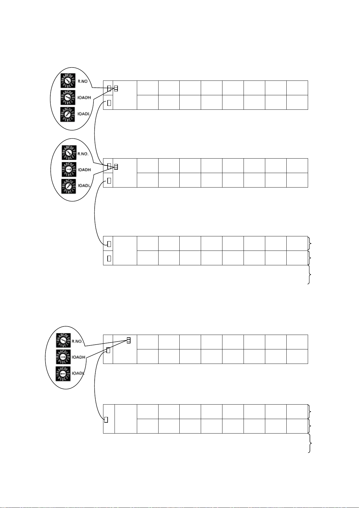
(3) I/O address allocation
A
A
Example 1 : For PC2/ L2
01234567
IN-22 IN-22 A/D D/A
vacancy
SIO IN-22
OUT-28
I/O
power
I/O
power
PC2/L2
CPU
32
points32points64points32points32points0point
32
points
32
points
1E0 200 220 260 280 2A0 2C0
| | | | | | |
1FF 21F 25F 27F 29F 2BF 2DF
01234567
IN-22 IN-22 IN-22
OUT-25 OUT-25
IN-22
OUT-28 OUT-29
32
points32points32points32points32points32points32points32points
0E0 100 120 140 160 180 1A0 1C0
| | | | | | | |
0FF 11F 13F 15F 17F 19F 1BF 1DF
01234567
PC-
LINK
IN-21 IN-21 IN-21 IN-21
OUT-21 OUT-21 OUT-21
0
point32points32points32points32points32points32points32points
000 020 040 060 080 0A0 0C0
| | | | | | |
01F 03F 05F 07F 09F 0BF 0DF
Module name
Occupied points
ddress
allocation
Example2 : For PC2J/3J
pow
er
Selector
PC2J
CPU
01234567
HPC-
LINK
IN-12 IN-12
OUT-15 OUT-15 OUT-15
IN-12
OUT-18
0
point16points16points16points16points16points16points16points
080 090 0A0 0B0 0C0 0D0 0E0
| | | | | | |
08F 09F 0AF 0BF 0CF 0DF 0EF
01234567
IN-22 IN-22 A/D D/A
vacancy
SIO IN-22
OUT-28
16
points16points16points16points16points16points16points16points
000 010 020 030 040 050 060 070
| | | | | | | |
00F 01F 02F 03F 04F 05F 06F 07F
1-3
Module name
Occupied
points
ddress
allocation
Page 31

1.2. Circuit diagram configuration
Usually, a circuit diagram represent ing sequence circuit including TOYOPUC is dra wn in a form of
relay circuit (ladder diagram). The figures below show recommendable expression of circuit
configuration which m ak e the d esign and maintenance of contr ol b oard e asi er.
Machine unit (A) Machine unit(B)
Input
section
Circuits and compon ents of the same function in a machine sh ould be represent ed in a respective
block, such as input, lo gic and outp ut sec tio n on a m achine bas is.
Logic
section
Output
section
Input
section
Logic
section
Output
section
1-4
Page 32

1.3. I/O circuit
1.3.1. Input section
Devices to whic h TOYOPUC sends input signals (suc h as pushbutton s witch and lim it switch) are
written in the i nput s ect ion.
Example of circ uit
Input(21)
Start
Original
Advanced end
Type
Input
Address
identifier
X
EX
PC3J
GX
PC3JG
Example of
address
X150
Example of s ymbol
(Contact)
1-5
Page 33

1.3.2. Output section
Devices to which TOYOPUC sends outputs (such as solenoid-operated
directional co ntro l va lve, elec tro-m agnet ic vale and m agne tic s witc h) are
written in outp ut sec tio n.
Example of circ uit
Output(21)
Advance
Retract
Spindle start
Type
Output
Address
identifier
Y
EY PC3J
GY
PC3JG
Example of
address
Y260
Example of s ymbol
(Coil) (Contact)
1-6
Page 34

1.4. Logic section
1.4.1. Internal relay (dummy output)
Internal rela y (dumm y output) f or tem porar y storag e whic h does not drive exter nal devices such as
solenoid-oper ated va lve or magnet ic swit ch is writ ten in logic sectio n.
Example of circ uit
Advance memorized
Type
Internal
relay
Address
identifier
M
EM
GM
PC3J
PC3JG
Example of
address
M000
Example of s ymbol
(Coil) (Contact)
1-7
Page 35

1.4.2. Timer
The timers used are divided into the following categories and are to be expressed in the logic
section.
Timer
Integrating
timer
Example of circ uit
Function
Direct setup
Indirect
setup
Direct setup
Indirect
setup
Mnemonic
Extended
Unit in 10ms TMRH ETMRH
Unit in
100ms
Unit in 10ms TMRH ETMRH
Unit in
100ms
Unit in 10ms TMRSH ETMRSH
Unit in
100ms
Unit in 10ms TMRSH ETMRSH
Unit in
100ms
TMR ETMR
TMR ETMR
TMRS ETMRS
TMRS ETMRS
End of advance tim er
0.2sec
PC3J
Type
Timer
Address
identifier
T
ET
PC3J
Example of
address
T012
Example of s ymbol
(Coil) (Contact)
T012
T012
1-8
Page 36

1.4.3. Counter
The counters use d are divided into the f ollowing categories and are to be expressed in t he logic
section.
Up counter
Down counter
Up/Down
counter
Example of circ uit
Function
Direct setup CNT ECNT
Indirect setup CNT ECNT
Direct setup CNTD ECNTD
Indirect setup CNTD ECNTD
Direct setup CNTH ECNTH
Indirect setup CNTH ECNTH
Mnemonic
Extended
PC3J
Type
Counter
Address
identifier
C
EC
PC3J
Example of
address
C051
Example of s ymbol
(Coil) (Contact)
1-9
Page 37

1.4.4. Keep relay
Relays used to h old th e curr ent c ondit io n whe n po wer is r em oved.
They are to be re presen ted i n the logic s ection.
Example of circ uit
Work finish setting
Work finish
Type
Keep relay
Address
identifier
K
EK
PC3J
Example of
address
K00A
Example of s ymbol
(Set coil) (Reset coil) (Contact)
1-10
Page 38

1.4.5. Edge detection
Turns on for a period equa l to one scan of sequence when c onditions are m et( )or not
met ( ). This part should be expressed in logic section.
Example of circ uit
Store set value
Setting switch
OFF pulse
Type
Edge
detection
(Note) T he addres s m ust not be used du plic atio n.
512 edge detection, P0 00 to P1FF, are possible.
4096 edge detecti on, E P000 to E PFFF, are possible.
Address
identifier
P
EP
PC3J
Example of
address
P001
Example of s ymbol
(Rise contact) (Fall contact)
1-11
Page 39

1.4.6. Special relay
Special relays are internal relays whose application and function are predetermined by the TOYOPUC, the
primary applications being to indicate operation status of this machine and result of arithmetic operation
made through application instruction.
Example of circuit
Type
Special relay
(1) In case of PC2/L2,PC2J
Of these relays, communication resets (V80-V87) are used as output (coil) and the remainders input
(contact).
Remember that the application of an out instruction to special relays other than V89-V87 results in
uncertain operation.
It is all reservation area for the address that doesn't exist in the list. Therefore, the user cannot use its
address.
Address
identifier
V
EV PC3J
Example of
address
V51
TOYOPUC
Battery error (flicker 1sec)
Data comparison
D1000<D1001
D1000=D1001
D1000>D1001
Example of symbol
(Coil) (Contact)
1-12
Page 40

Address
V01 MAJOR ERROR
V02 MINOR ERROR
V03 ALARM
V04 NORMALLY ON Normally 1 Normally ON irrespective of run status.
V05 NORMALLY OFF Normally 0 Normally OFF irrespective of run status.
V06 1ST SCAN
User mode key input
V07
PC2/L2
V08#Memory card mounting
PC2/L2
V20#Program card mode
PC2/L2
V21#Data car d m od e
PC2/L2
I/O monitor user mode
V22
PC2/L2
V23 Debug mode
V24 During dummy stop
Request for stop
V25
continued
V26 Stopped
V27 RUN
V30 1-instruction step
V31 1-block step
V32 1-scan step
V33 Trigger detection
V34 Enable detection
Name Outline Description
0: No ERR0
1: ERR0 in occurring
0: No ERR1
1: ERR1 in occurring
0: No ALM
1: ALM in outputting
END command
ON
Reset
OFF
0:Key input not contained
1:Key input contained
0:Memory card is not mounted
1:Memory card is mounted
0:Other than program card
mode
1:In program card mode
0:Other than data card mode
1:In data card mode
0:I/O monitor mode
1:User mode
0:Not debug mode
1:In debug mode
0:Not during dummy stop
1:During dummy stop
0:Request for stop not issued
1:Request for stop issued
0:Scanning
1:Stopped
0:Sequence instruction not
executed
1:Sequence instruction
executed
0:1-instruction step not in
progress
1:1-instruction step in progress
0:1-block step not in progress
1:1-block step in progress
0:1-scan step not in progress
1:1-scan step in progress
0:Trigger not detected
1:Trigger detected
0:Enable not detected
1:Enable detected
ON against occurrence of major error
OFF after ERROR is reset
ON against occurrence of minor error.
OFF after ERROR is reset.
ON against ALARM
OFF after ERROR is reset.
ON by resetting and OFF by END
processing.
Turns ON if there is key input when the I/O
monitor is in the user mode and OFF when
the key input of the application instruction
is executed.
Turns ON when the memory card is
mounted
Turns ON by program card mode setting
and OFF by CPU RAM or data card mode
setting.
Turns ON by data card mode setting and
OFF by CPU RAM or program card mode
setting.
Turns ON when the I/O monitor is in the
user mode and OFF when in the I/O
monitor mode
Turns ON by the debug mode setting and
OFF when error reset
Turns ON when the dummy scan stop is
executed and OFF when error reset
Turn ON by a request for scan stop and OF
when error request
OFF during sequence scan and ON during
stepping
ON during sequence scan
ON while 1-instruction step is in progress
ON while 1-block step is in progress
ON while 1-scan step is in progress
Turn ON when the trace starts and OFF
when the trigger instruction is executed
after an enable is detected.
Turns OFF when the trace starts and ON
when the enable instruction is executed
# : Can be used with SCPU-4.10 or later version CPU.
(WCPU version is irrelevant)
1-13
Page 41

Address
Name Outline Description
V35 Time trace
V36 Scan trace
V37 Instruction trace
V3D Status latch setting
V3F I/O off-line
APPLIED COMMAND
V50
ERROR 1
(ER)
V51 <
V52 =
V53 >
V54 ZERO (Z)
V55 BORROW (BO)
V56 CARRY (CY)
V70 0.1 SEC CLOCK
V71 0.2 SEC CLOCK
V72 1-SEC CLOCK
V73 2-SEC CLOCK
V74 60-SEC CLOCK
V78 SCAN CLOCK
USER DEFINED CLOCK 1
V79
USER DEFINED CLOCK 2
V7A
COMMUNICATION RESET
V80
No.1
COMMUNICATION RESET
V81
No.2
COMMUNICATION RESET
V82
No.3
COMMUNICATION RESET
V83
No.4
COMMUNICATION RESET
V84
No.5
COMMUNICATION RESET
V85
No.6
COMMUNICATION RESET
V86
No.7
COMMUNICATION RESET
V87
No.8
0:Not tracing
1:Tracing
0:Not tracing
1:Tracing
0:Not tracing
1;Tracing
0:Not set
1:Set
0:Not off-line
1:Off-line processing
0: No error
1: Error
0: Comparative result not small
1: Comparative result small
0: Comparative result unequal
1: Comparative result equal
0: Comparative result not large
1: Comparative result large
0: Result not 0
1: Result 0
0: No digit down
1: Digit down
0: No digit up
1: Digit up
0.05 sec
0.05 sec
0.1 sec
0.1 sec
0.5 sec
0.5 sec
1 sec
1 sec
30 sec
30 sec
1 scan
n scan
n scan
1 scan
m scan
m scan
0: RESET OFF
1: RESET ON
0: RESET OFF
1: RESET ON
0: RESET OFF
1: RESET ON
0: RESET OFF
1: RESET ON
0: RESET OFF
1: RESET ON
0: RESET OFF
1: RESET ON
0: RESET OFF
1: RESET ON
0: RESET OFF
1: RESET ON
Turn ON when the time trace starts and
when it ends.
Turns ON when the scan trace starts and
OFF it ends
Turns ON when the instruction trace starts
and OFF when it ends
Turns On when the status latch execution
is specified.
ON during I/O off-line processing.
ON if applied command error occurs and
OFF if not, but limited to only command
with confinement .
Result of comparison with applied
command
Result of comparison with applied
command
Result of comparison with applied
command
ON when computation result of applied
command is 0.
The computation result of applied
command is smaller than 0.
The computation result of applied
command exceeded the specific digit
number.
Clock of cycle 0.1 sec and duty 50%
Clock of cycle 0.2 sec and duty 50%
Clock of cycle 1 sec and duty 50%
Clock of cycle 2 sec and duty 50%
Clock of cycle 60 sec and duty 50%
Clock to turn ON/ OFF SCAN every 1 scan.
Clock to turn ON/OFF scan at scanning
interval preset by applied command.
Clock to turn ON/OFF scan at scanning
interval preset by applied command.
1-14
Page 42

Address
V90
V91
V92
V93
V94
V95
V96
V97
V98
V99
V9A
V9B
V9C
V9D
V9E
V9F
VA0
VA1
VA2
LINK1 COMMAND USE PERMIT
FLAG
LINK1 COMMAND ERROR FLAG
LINK2 COMMAND USE PERMIT
FLAG
LINK2 COMMAND ERROR FLAG
LINK3 COMMAND USE PERMIT
FLAG
LINK3 COMMAND ERROR FLAG
LINK4 COMMAND USE PERMIT
FLAG
LINK4 COMMAND ERROR FLAG
LINK5 COMMAND USE PERMIT
FLAG
LINK5 COMMAND ERROR FLAG
LINK6 COMMAND USE PERMIT
FLAG
LINK6 COMMAND ERROR FLAG
LINK7 COMMAND USE PERMIT
FLAG
LINK7 COMMAND ERROR FLAG
LINK8 COMMAND USE PERMIT
FLAG
LINK8 COMMAND ERROR FLAG
ALL ST IN COMMUNICATING
LINK PARAMETER ERROR
COMMUNICATION ERROR
Name Outline Description
VA3
ALL ST IN COMMUNICATING
VA4
LINK PARAMETER ERROR
VA5
COMMUNICATION ERROR
VA6
VA7
ALL ST IN COMMUNICATING
VA8
LINK PARAMETER ERROR
VA9
COMMUNICATION ERROR
VAA
VAB
ALL ST IN COMMUNICATING
VAC
LINK PARAMETER ERROR
VAD
COMMUNICATION ERROR
VAE
VAF
ALL ST IN COMMUNICATING
VB0
LINK PARAMETER ERROR
VB1
COMMUNICATION ERROR
VB2
VB3
ALL ST IN COMMUNICATING
VB4
LINK PARAMETER ERROR
VB5
COMMUNICATION ERROR
VB6
VB7
ALL ST IN COMMUNICATING
VB8
LINK PARAMETER ERROR
VB9
COMMUNICATION ERROR
VBA
VBB
ALL ST IN COMMUNICATING
VBC
LINK PARAMETER ERROR
VBD
COMMUNICATION ERROR
VBE
VBF
VC0 CPU ERR OR
VC1 POW ER DOW N
VC2 ME MORY DATA ERROR
VC3 I/O BUS ERR OR
SPECIAL MODULE
VC4
ERROR
No.1
No.2
No.3
No.4
No.5
No.6
No.7
No.8
0: No error
1: Error
0: No error
1: Error
0: No error
1: Error
0: No error
1: Error
0: No error
1: Error
0: No error
1: Error
0: No error
1: Error
0: No error
1: Error
0: No error
1: Error
0: No error
1: Error
0: No error
1: Error
0: No error
1: Error
0: No error
1: Error
ON upon detection of CPU module error.
ON upon detection of POWER DOWN .
OFF after reset or power on
ON detection of program or parameter data
error.
ON upon detection of I/O bus error.
ON upon detection of special module error
OFF after ERROR reset
1-15
Page 43

Address
VC5
MODULE PARAMETER
ERROR
Name Outline Description
VC6 PARAMETER ERROR
I/O MODULE ERROR
VC7
( Fuse blown, etc.)
I/O COMPOSITION
VC8
ERROR
USER PROGRAM
VC9
ERROR
MEMORY CARD ERROR
VCA
PC2/L2
I/O VERIFICATION
VE0
ERROR
VE1 SCAN TIME-OVER
Arithmetic operation
VE2
instruction error
VF0 BATTERY ERROR
Memory card battery error
VF1
PC2/L2
SPECIAL MODULE
VF2
ALLOCATION ERROR
0: No error
1: Error
0: No error
1: Error
0: No error
1: Error
0: No error
1: Error
0: No error
1: Error
0: No error
1: Error
0: No error
1: Error
0: No error
1: Error
0: No error
1: Error
0: No error
1: Error
0: No error
1: Error
0: No error
1: Error
ON when CPU can not recognize correctly
I/O module.
ON upon detection of parameter error.
ON upon detection of I/O module error
OFF after ERROR reset
ON upon detection of I/O module composition
error/
( Allocation of special card number and I/O
addresses )
ON upon detection of error related to user
program. OFF after ERROR reset.
Turns ON when an error related to the
memory card is detected and OFF when
reset or power is supplied.
ON when I/O identification codes of
parameter differ from actually mounted I/O
modules.
ON upon detection of SCAN TIME OVER .
OFF after reset or power on
Turns ON when an application instruction
error is detected and OFF when error reset
or 0 is set.
ON upon error detection
OFF after ERROR reset
ON upon error detection
OFF after ERROR reset
ON against allocation error of
communication (link) module.
1-16
Page 44

(2) In case of PC3J
Special relays are used for special applications such as CPU status, applied commands,
link module, etc. And these relays exist in the basic area and the extended area.
For the data memory separate mode the special relays are provided in the basic area
every each program. In this case, applied-command related special relays which are used
in each sequence program are configured in special-relay area corresponding to the
program. Other relays are all configured in the special relay area for " PRG.1".
Don't handle a user because "V58~V5D" "EV800~EVBFF" is used for the one for the
executive control of SFC when you do programming by SFC.
It is all reservation area for the address that doesn't exist in the list. Therefore, the user
cannot use its address.
(2-1) Data memory separate mode PRG.1
Address
V01 MAJOR ERROR
V02 MINOR ERROR
V03 ALARM
V04 NORMALLY ON Normally 1 Normally ON irrespective of run status.
V05 NORMALLY OFF Normally 0 Normally OFF irrespective of run status.
V06 1ST SCAN
IN DUMMY
V24
STOPPING
STOP REQ IN
V25
CONTINUING
V26 IN STOPPING
V27
RUN
DATA MEMORY
V38
MODE
PRG.1 FUN FLAG
V39
CLEAR MODE
V3A IN DATA BACK-UP
V40
PRG.1
V41
PRG.2
V42
PRG.3
Name Outline Description
RUN
RUN
RUN
0: No ERR0
1: ERR0 in occurring
0: No ERR1
1: ERR1 in occurring
0: No ALM
1: ALM in outputting
END command
ON
Reset
OFF
0: Not in dummy stopping
1: In dummy stopping
0: No stop request
1: Stop requested
0: In scanning
1: In stopping
0: Sequence command
non-execution
1: Sequence command in executing
0: Single mode
1: Division mode
0: Not FUN FLAG CLEAR
MODE
1: FUN FLAG CLEAR MODE
0: Not in data backing up
1: In data backing-up
0: Sequence command
non-execution
1: Sequence command in executing
0: Sequence command
non-execution
1: Sequence command in executing
0: Sequence command
non-execution
1: Sequence command in executing
ON against occurrence of major error
OFF after ERROR is reset
ON against occurrence of minor error.
OFF after ERROR is reset.
ON against ALARM
OFF after ERROR is reset.
ON by resetting and OFF by END
processing.
ON by executing dummy scan stop
OFF by resetting
ON by dummy scan stop request.
OFF by resetting
OFF during sequence scan
But ON during step-operation
ON while sequence command is in
executing.
ON under data area division mode
ON when program-1 is FUN FLAG CLEAR
mode.
ON while user data is being backed up
ON while program-1 is executing sequence
command.
ON while program-2 is executing sequence
command.
ON while program-3 is executing sequence
command.
1-17
Page 45

Address
PRG.1 APPLIED
COMMAND ERROR 1
V50
(ER)
V51 PRG.1 <
V52 PRG.1 =
V53 PRG.1 >
V54 PRG.1 ZERO (Z)
V55 PRG.1 BORROW (BO)
V56 PRG.1 CARRY (CY)
V5E DATA ERROR CLEAR 1: Data error clea red
V5F DATA BA CKUP START
Name Outline Description
0: No error
1: Error
0: Comparative result not
small
1: Comparative result small
0: Comparative result
unequal
1: Comparative result
equal
0: Comparative result not
large
1: Comparative result large
0: Result not 0
1: Result 0
0: No digit down
1: Digit down
0: No digit up
1: Digit up
ON if applied command error occurs in
program-1 and OFF if not, but limited to only
command with confinement .
Result of comparison wit h appli ed comma nd in
program-1
Result of comparison wit h appli ed comma nd in
program-1
Result of comparison wit h appli ed comma nd in
program-1
ON when computation result of applied
command in program-1 is 0.
The computation result of applied command in
program-1 is smaller than 0.
The computation result of applied command in
program-1 exceeded the specific digit number.
DATA ERROR UNCHECK ALM is cleared by
turning ON this special relay (V5E).
Back-up start
with fall
USER DATA BACK-UP is started by ON->OFF
of this special relay (V5F). V3A keeps ON
while the back-up is being executed.
V70 0.1 SEC CLOCK
V71 0.2 SEC CLOCK
V72 1-SEC CLOCK
V73 2-SEC CLOCK
V74 60-SEC CLOCK
V78 SCAN CLOCK
USER DEFINED CLOCK 1
V79
USER DEFINED CLOCK 2
V7A
Prg.1-Link1
V80
COMMUNICATION RESET
Prg.1-Link2
V81
COMMUNICATION RESET
Prg.1-Link3
V82
COMMUNICATION RESET
Prg.1-Link4
V83
COMMUNICATION RESET
Prg.1-Link5
V84
COMMUNICATION RESET
Prg.1-Link6
V85
COMMUNICATION RESET
Prg.1-Link7
V86
COMMUNICATION RESET
Prg.1-Link8
V87
COMMUNICATION RESET
0.05 sec
0.05 sec
0.1 sec
0.1 sec
0.5 sec
0.5 sec
1 sec
1 sec
30 sec
30 sec
1 scan
n scan
n scan
1 scan
m scan
m scan
0: RESET OFF
1: RESET ON
0: RESET OFF
1: RESET ON
0: RESET OFF
1: RESET ON
0: RESET OFF
1: RESET ON
0: RESET OFF
1: RESET ON
0: RESET OFF
1: RESET ON
0: RESET OFF
1: RESET ON
0: RESET OFF
1: RESET ON
Clock of cycle 0.1 sec and duty 50%
Clock of cycle 0.2 sec and duty 50%
Clock of cycle 1 sec and duty 50%
Clock of cycle 2 sec and duty 50%
Clock of cycle 60 sec and duty 50%
Clock to turn ON/ OFF SCAN every 1 scan.
Clock to turn ON/OFF scan at scanning interval
preset by applied command.
Clock to turn ON/OFF scan at scanning interval
preset by applied command.
Note) For the communication (link) modules, see the respective Instruction Manuals.
1-18
Page 46

Address
V90
V91
V92
V93
V94
V95
V96
V97
V98
V99
V9A
V9B
V9C
V9D
V9E
V9F
VA0
VA1
VA2
VA3
VA4
VA5
VA6
VA7
VA8
VA9
VAA
VAB
VAC
VAD
VAE
VAF
VB0
VB1
VB2
VB3
VB4
VB5
VB6
VB7
VB8
VB9
VBA
VBB
VBC
VBD
VBE
VBF
LINK COMMAND USE
PERMIT FLAG
LINK COMMAND
ERROR FLAG
LINK COMMAND USE
PERMIT FLAG
LINK COMMAND
ERROR FLAG
LINK COMMAND USE
PERMIT FLAG
LINK COMMAND
ERROR FLAG
LINK COMMAND USE
PERMIT FLAG
LINK COMMAND
ERROR FLAG
LINK COMMAND USE
PERMIT FLAG
LINK COMMAND
ERROR FLAG
LINK COMMAND USE
PERMIT FLAG
LINK COMMAND
ERROR FLAG
LINK COMMAND USE
PERMIT FLAG
LINK COMMAND
ERROR FLAG
LINK COMMAND USE
PERMIT FLAG
LINK COMMAND
ERROR FLAG
ALL ST IN
COMMUNICATING
LINK PARAMETER
ERROR
COMMUNICATION
ERROR
ALL ST IN
COMMUNICATING
LINK PARAMETER
ERROR
COMMUNICATION
ERROR
ALL ST IN
COMMUNICATING
LINK PARAMETER
ERROR
COMMUNICATION
ERROR
ALL ST IN
COMMUNICATING
LINK PARAMETER
ERROR
COMMUNICATION
ERROR
ALL ST IN
COMMUNICATING
LINK PARAMETER
ERROR
COMMUNICATION
ERROR
ALL ST IN
COMMUNICATING
LINK PARAMETER
ERROR
COMMUNICATION
ERROR
ALL ST IN
COMMUNICATING
LINK PARAMETER
ERROR
COMMUNICATION
ERROR
ALL ST IN
COMMUNICATING
LINK PARAMETER
ERROR
COMMUNICATION
ERROR
Name Outline Description
ü
Prg.1-
ý
Link 1
þ
ü
Prg.1-
ý
Link2
þ
ü
Prg.1-
ý
Link3
þ
ü
Prg.1-
ý
Link4
þ
ü
Prg.1-
ý
Link5
þ
ü
Prg.1-
ý
Link6
þ
ü
Prg.1-
ý
Link7
þ
ü
Prg.1-
ý
Link8
þ
ü
ï
Prg.1Link1
Prg.1Link2
Prg.1Link3
Prg.1Link4
Prg.1Link5
Prg.1Link6
Prg.1Link7
Prg.1Link8
0: No error
1: Error
0: No error
1: Error
0: No error
1: Error
0: No error
1: Error
0: No error
1: Error
0: No error
1: Error
0: No error
1: Error
0: No error
1: Error
ý
ï
þ
ü
ï
ý
ï
þ
ü
ï
ý
ï
þ
ü
ï
ý
ï
þ
ü
ï
ý
ï
þ
ü
ï
ý
ï
þ
ü
ï
ý
ï
þ
ü
ï
ý
ï
þ
Note) For the communication (link) modules, see the respective Instruction Manuals.
1-19
Page 47

Address
Name Outline Description
VC0 CPU ERR OR
VC1 POW ER DOW N
MEMORY DATA
VC2
ERROR
VC3 I/O BUS ERR OR
SPECIAL MODULE
VC4
ERROR
MODULE PARAMETER
VC5
ERROR
VC6 PARAMETER ERROR
I/O MODULE ERROR
VC7
( Fuse blown, etc.)
I/O COMPOSITION
VC8
ERROR
USER PROGRAM
VC9
ERROR
BACK UP MEMORY
VCA
ERROR
DATA ERROR
VCB
UNCHECK
PRG.1
VD0
USER PROGRAM ERROR
PRG.2
VD1
USER PROGRAM ERROR
PRG.3
VD2
USER PROGRAM ERROR
PRG.1 PARAMETER
VD8
ERROR
PRG.2 PARAMETER
VD9
ERROR
PRG.3 PARAMETER
VDA
ERROR
I/O VERIFICATION
VE0
ERROR
VE1 SCAN TIME-OVER
PRG.1 APPLIED
VE2
COMMAND ERROR
LATCH
PRG.1 SCAN TIME
VE8
OVER
PRG.2 SCAN TIME
VE9
OVER
PRG.3 SCAN TIME
VEA
OVER
VF0 BATTERY ERROR
SPECIAL MODULE
VF2
ALLOCATION ERROR
DIAGNOSIS MODULE
VF3
ERROR
VF5 BATTERY ERROR
0: No error
1: Error
0: No error
1: Error
0: No error
1: Error
0: No error
1: Error
0: No error
1: Error
0: No error
1: Error
0: No error
1: Error
0: No error
1: Error
0: No error
1: Error
0: No error
1: Error
0: No error
1: Error
0: checked
1: uncheck
0: No error
1: Error
0: No error
1: Error
0: No error
1: Error
0: No error
1: Error
0: No error
1: Error
0: No error
1: Error
0: No error
1: Error
0: No error
1: Error
0: No error
1: Error
0: No error
1: Error
0: No error
1: Error
0: No error
1: Error
0: No error
1: Error
0: No error
1: Error
0: No error
1: Error
0: No error
1: Error
ON upon detection of CPU module error.
ON upon detection of POWER DOWN .
OFF after reset or power on
ON detection of program or parameter data
error.
ON upon detection of I/O bus error.
ON upon detection of special module error
OFF after ERROR reset
ON when CPU can not recognize correctly I/O
module.
ON upon detection of parameter error.
ON upon detection of I/O module error
OFF after ERROR reset
ON upon detection of I/O module composition error/
( Allocation of special card number and I/O
addresses )
ON upon detection of error related to user
program. OFF after ERROR reset.
ON upon detection of back-up memory error
ON upon detection of memory data error (VC2).
OFF with V5E ON or use of peripheral
equipment.
ON upon errors related to user program as
program-1
ON upon errors related to user program as
program-2
ON upon errors related to user program as
program-3
ON upon detection of program-1 parameter
error
ON upon detection of program-2 parameter
error
ON upon detection of program-3 parameter
error
ON when I/O identification codes of parameter
differ from actually mounted I/O modules.
ON upon detection of SCAN TIME OVER .
OFF after reset or power on
ON against occurrence of error of applied
command (V50) in program-1. It is held until
reset or 0 write.
ON upon detection of scan time-over in
program-1. OFF after reset or power on
ON upon detection of scan time-over in
program-2. OFF after reset or power on
ON upon detection of scan time-over in
program-3. OFF after reset or power on
ON upon error detection
OFF after ERROR reset
ON against allocation error of communication
(link) module.
ON against diagnosis module error.
ON upon detection of built-in clock error.
1-20
Page 48

(2-2) Data memory separate mode PRG.2
Address
Name Outline Description
V04 NORMALLY ON NORMALLY 1 ON irrespective operation status
V05 NORMALLY OFF NORMALLY 0 OFF irrespective of operation status
END command
V06 1ST SCAN
ON
Reset
ON by resetting and OFF by END processing.
OFF
V24 IN DUMMY STOPPING
IN STOP REQUEST
V25
CONTINUING
V26 IN STOPPING
PRG.2 FUN FLAG
V39
CLEAR MODE
PRG.2 APPLIED
COMMAND ERROR 1
V50
(ER)
V51 PRG.2 <
V52 PRG.2 =
V53 PRG.2 >
V54 PRG.2 ZERO (Z)
V55 PRG.2 BORROW (BO)
V56 PRG.2 CARRY (CY)
V70 0.1 SEC CLOCK
V71 0.2 SEC CLOCK
V72 1-SEC CLOCK
V73 2-SEC CLOCK
V74 60-SEC CLOCK
V78 SCAN CLOCK
USER DEFINED CLOCK
V79
1
USER DEFINED CLOCK
V7A
2
0: Not in dum my s topping
1: In dummy stopping
0: No stop reque st
1: Stop requested
0: In scanning
1: In stopping
0: Not FUN FLAG CLEAR MODE
1: FUN FLAG CLEAR MODE
0: No error
1: Error
0: Comparative result not small
1: Comparative result small
0: Comparative result unequal
1: Comparative result equal
0: Comparative result not large
1: Comparative result large
0: Result not 0
1: Result 0
0: No digit down
1: Digit down
0: No digit up
1: Digit up
0.05 sec
0.05 sec
0.1 sec
0.1 sec
0.5 sec
0.5 sec
1 sec
1 sec
30 sec
30 sec
1 scan
n scan
n scan
1 scan
m scan
m scan
ON by executing dummy scan stop
OFF by resetting
ON by dummy scan stop request.
OFF by resetting
OFF during sequence scan
But ON during step-operation
ON when program-2 is FUN FLAG CLEAR
mode.
ON if applied command error occurs in
program-2 and OFF if not, but limited to only
command with confinement .
Result of comparison wit h appli ed comma nd in
program-2
Result of comparison wit h appli ed comma nd in
program-2
Result of comparison wit h appli ed comma nd in
program-2
ON when computation result of applied
command in program-2 is 0.
The computation result of applied command in
program-2 is smaller than 0.
The computation result of applied command in
program-2 exceeded the specific digit number.
Clock of cycle 0.1 sec and duty 50%
Clock of cycle 0.2 sec and duty 50%
Clock of cycle 1 sec and duty 50%
Clock of cycle 2 sec and duty 50%
Clock of cycle 60 sec and duty 50%
Clock to turn ON/ OFF SCAN every 1 scan.
Clock to turn ON/OFF scan at scanning interval
preset by applied command.
Clock to turn ON/OFF scan at scanning interval
preset by applied command.
1-21
Page 49

Address
V80
V81
V82
V83
V84
V85
V86
V87
V90
V91
V92
V93
V94
V95
V96
V97
V98
V99
V9A
V9B
V9C
V9D
V9E
V9F
VA0
VA1
VA2
Prg2-Link1
COMMUNICATION RESET
Prg2-Link2
COMMUNICATION RESET
Prg2-Link3
COMMUNICATION RESET
Prg2-Link4
COMMUNICATION RESET
Prg2-Link5
COMMUNICATION RESET
Prg2-Link6
COMMUNICATION RESET
Prg2-Link7
COMMUNICATION RESET
Prg2-Link8
COMMUNICATION RESET
LINK COMMAND
USE PERMIT FLAG
LINK COMMAND
ERROR FLAG
LINK COMMAND
USE PERMIT FLAG
LINK COMMAND
ERROR FLAG
LINK COMMAND
USE PERMIT FLAG
LINK COMMAND
ERROR FLAG
LINK COMMAND
USE PERMIT FLAG
LINK COMMAND
ERROR FLAG
LINK COMMAND
USE PERMIT FLAG
LINK COMMAND
ERROR FLAG
LINK COMMAND
USE PERMIT FLAG
LINK COMMAND
ERROR FLAG
LINK COMMAND
USE PERMIT FLAG
LINK COMMAND
ERROR FLAG
LINK COMMAND
USE PERMIT FLAG
LINK COMMAND
ERROR FLAG
ALL ST IN
COMMUNICATING
LINK PARAMETER
ERROR
COMMUNICATION
ERROR
Name Outline Description
0: RESET OFF
1: RESET ON
0: RESET OFF
1: RESET ON
0: RESET OFF
1: RESET ON
0: RESET OFF
1: RESET ON
0: RESET OFF
1: RESET ON
0: RESET OFF
1: RESET ON
0: RESET OFF
1: RESET ON
0: RESET OFF
1: RESET ON
ü
Prg2-
ý
Link1
þ
ü
Prg2-
ý
Link2
þ
ü
Prg2-
ý
Link3
þ
ü
Prg2-
ý
Link4
þ
ü
Prg2-
ý
Link5
þ
ü
Prg2-
ý
Link6
þ
ü
Prg2-
ý
Link7
þ
ü
Prg2-
ý
Link8
þ
ü
ï
Prg2Link1
0: No error
1: Error
ý
ï
þ
VA3
ALL ST IN
VA4
VA5
VA6
COMMUNICATING
LINK PARAMETER
ERROR
COMMUNICATION
ERROR
ü
ï
Prg2-
ý
Link2
ï
þ
0: No error
1: Error
VA7
ALL ST IN
VA8
VA9
VAA
COMMUNICATING
LINK PARAMETER
ERROR
COMMUNICATION
ERROR
ü
ï
Prg2-
ý
Link3
ï
þ
0: No error
1: Error
VAB
ALL ST IN
VAC
VAD
VAE
COMMUNICATING
LINK PARAMETER
ERROR
COMMUNICATION
ERROR
ü
ï
Prg2-
ý
Link4
ï
þ
0: No error
1: Error
VAF
Note) For the communication (link) modules, see the respective Instruction Manuals.
1-22
Page 50

Address
VB0
VB1
VB2
ALL ST IN
COMMUNICATING
LINK PARAMETER
ERROR
COMMUNICATION
ERROR
Name Outline Description
ü
ï
Prg2Link5
0: No error
1: Error
ý
ï
þ
VB3
ALL ST IN
VB4
VB5
VB6
COMMUNICATING
LINK PARAMETER
ERROR
COMMUNICATION
ERROR
ü
ï
Prg2-
ý
Link6
ï
þ
0: No error
1: Error
VB7
ALL ST IN
VB8
VB9
VBA
COMMUNICATING
LINK PARAMETER
ERROR
COMMUNICATION
ERROR
ü
ï
Prg2-
ý
Link7
ï
þ
0: No error
1: Error
VBB
ALL ST IN
VBC
VBD
VBE
COMMUNICATING
LINK PARAMETER
ERROR
COMMUNICATION
ERROR
ü
ï
Prg2-
ý
Link8
ï
þ
0: No error
1: Error
VBF
PRG.2 APPLIED
VE2
COMMAND LATCH
ERROR
0: No error
1: Error
ON against occurrence of applied command
error (V50) in program-2 and it is held until reset
or 0 write.
(Note) For the communication (link) modules, see the respective Instruction Manuals.
1-23
Page 51

(2-3) Data memory separate mo de PRG.3
Address
V04 NORMALLY ON NORMALLY 1 ON irrespective operation status
V05 NORMALLY OFF NORMALLY 0 OFF irrespective of operation status
V06 1ST SCAN
V24 IN DUMMY STOPPING
IN STOP REQUEST
V25
CONTINUING
V26 IN STOPPING
PRG.3 FUN FLAG
V39
CLEAR MODE
PRG.3 APPLIED
COMMAND ERROR 1
V50
(ER)
V51 PRG.3 <
V52 PRG.3 =
V53 PRG.3 >
V54 PRG.3 ZERO (Z)
V55 PRG.3 BORROW (BO)
V56 PRG.3 CARRY (CY)
V70 0.1 SEC CLOCK
V71 0.2 SEC CLOCK
V72 1-SEC CLOCK
V73 2-SEC CLOCK
V74 60-SEC CLOCK
V78 SCAN CLOCK
USER DEFINED CLOCK
V79
1
USER DEFINED CLOCK
V7A
2
Name Outline Description
END command
ON
Reset
ON by resetting and OFF by END processing.
OFF
0: Not in dummy stoppin g
1: In dummy stoppin g
0: No stop request
1: Stop requested
0: In scanning
1: In stopping
0: Not FUN FLAG CL EAR MO DE
1: FUN FLAG CLEAR MODE
0: No error
1: Error
0: Comparative result not sm all
1: Comparative result small
0: Comparative result unequal
1: Comparative result equal
0: Comparative result not large
1: Comparative result large
0: Result not 0
1: Result 0
0: No digit down
1: Digit down
0: No digit up
1: Digit up
0.05 sec
0.05 sec
0.1 sec
0.1 sec
0.5 sec
0.5 sec
1 sec
1 sec
30 sec
30 sec
1 scan
n scan
n scan
1 scan
m scan
m scan
ON by executing dummy scan stop
OFF by resetting
ON by dummy scan stop request.
OFF by resetting
OFF during sequence scan
But ON during step-operation
ON when program-3 is FUN FLAG CLEAR
mode.
ON if applied command error occurs in
program-2 and OFF if not, but limited to only
command with confinement .
Result of comparison wit h appli ed comma nd in
program-3
Result of comparison wit h appli ed comma nd in
program-3
Result of comparison wit h appli ed comma nd in
program-3
ON when computation result of applied
command in program-3 is 0.
The computation result of applied command in
program-3 is smaller than 0.
The computation result of applied command in
program-3 exceeded the specific digit number.
Clock of cycle 0.1 sec and duty 50%
Clock of cycle 0.2 sec and duty 50%
Clock of cycle 1 sec and duty 50%
Clock of cycle 2 sec and duty 50%
Clock of cycle 60 sec and duty 50%
Clock to turn ON/ OFF SCAN every 1 scan.
Clock to turn ON/OFF scan at scanning interval
preset by applied command.
Clock to turn ON/OFF scan at scanning interval
preset by applied command.
1-24
Page 52

Address
V80
V81
V82
V83
V84
V85
V86
V87
V90
V91
V92
V93
V94
V95
V96
V97
V98
V99
V9A
V9B
V9C
V9D
V9E
V9F
VA0
VA1
VA2
Prg3-Link1
COMMUNICATION RESET
Prg3-Link2
COMMUNICATION RESET
Prg3-Link3
COMMUNICATION RESET
Prg3-Link4
COMMUNICATION RESET
Prg3-Link5
COMMUNICATION RESET
Prg3-Link6
COMMUNICATION RESET
Prg3-Link7
COMMUNICATION RESET
Prg3-Link8
COMMUNICATION RESET
LINK COMMAND
USE PERMIT FLAG
LINK COMMAND
ERROR FLAG
LINK COMMAND
USE PERMIT FLAG
LINK COMMAND
ERROR FLAG
LINK COMMAND
USE PERMIT FLAG
LINK COMMAND
ERROR FLAG
LINK COMMAND
USE PERMIT FLAG
LINK COMMAND
ERROR FLAG
LINK COMMAND
USE PERMIT FLAG
LINK COMMAND
ERROR FLAG
LINK COMMAND
USE PERMIT FLAG
LINK COMMAND
ERROR FLAG
LINK COMMAND
USE PERMIT FLAG
LINK COMMAND
ERROR FLAG
LINK COMMAND
USE PERMIT FLAG
LINK COMMAND
ERROR FLAG
ALL ST IN
COMMUNICATING
LINK PARAMETER
ERROR
COMMUNICATION
ERROR
Name Outline Description
0: RESET OFF
1: RESET ON
0: RESET OFF
1: RESET ON
0: RESET OFF
1: RESET ON
0: RESET OFF
1: RESET ON
0: RESET OFF
1: RESET ON
0: RESET OFF
1: RESET ON
0: RESET OFF
1: RESET ON
0: RESET OFF
1: RESET ON
ü
Prg3-
ý
Link1
þ
ü
Prg3-
ý
Link2
þ
ü
Prg3-
ý
Link3
þ
ü
Prg3-
ý
Link4
þ
ü
Prg3-
ý
Link5
þ
ü
Prg3-
ý
Link6
þ
ü
Prg3-
ý
Link7
þ
ü
Prg3-
ý
Link8
þ
ü
ï
Prg3Link1
0: No error
1: Error
ý
ï
þ
VA3
ALL ST IN
VA4
VA5
VA6
COMMUNICATING
LINK PARAMETER
ERROR
COMMUNICATION
ERROR
ü
ï
Prg3-
ý
Link2
ï
þ
0: No error
1: Error
VA7
ALL ST IN
VA8
VA9
VAA
COMMUNICATING
LINK PARAMETER
ERROR
COMMUNICATION
ERROR
ü
ï
Prg3-
ý
Link3
ï
þ
0: No error
1: Error
VAB
ALL ST IN
VAC
VAD
VAE
COMMUNICATING
LINK PARAMETER
ERROR
COMMUNICATION
ERROR
ü
ï
Prg3-
ý
Link4
ï
þ
0: No error
1: Error
VAF
Note) For the communication (link) modules, see the respective Instruction Manuals.
1-25
Page 53

Address
VB0
VB1
VB2
ALL ST IN
COMMUNICATING
LINK PARAMETER
ERROR
COMMUNICATION
ERROR
Name Outline Description
ü
ï
Prg3Link5
0: No error
1: Error
ý
ï
þ
VB3
ALL ST IN
VB4
VB5
VB6
COMMUNICATING
LINK PARAMETER
ERROR
COMMUNICATION
ERROR
ü
ï
Prg3-
ý
Link6
ï
þ
0: No error
1: Error
VB7
ALL ST IN
VB8
VB9
VBA
COMMUNICATING
LINK PARAMETER
ERROR
COMMUNICATION
ERROR
ü
ï
Prg3-
ý
Link7
ï
þ
0: No error
1: Error
VBB
ALL ST IN
VBC
VBD
VBE
COMMUNICATING
LINK PARAMETER
ERROR
COMMUNICATION
ERROR
ü
ï
Prg3-
ý
Link8
ï
þ
0: No error
1: Error
VBF
PRG.3 APPLIED
VE2
COMMAND LATCH
ERROR
0: No error
1: Error
ON against occurrence of applied command
error (V50) in program-3 and it is held until reset
or 0 write.
(Note) For the communication (link) modules, see the respective Instruction Manuals.
1-26
Page 54

(2-4) Data memory single mode, basic area
Address Name Outline Description
V01 MAJOR ERROR
V02 MINOR ERROR
V03 ALARM
V04 NORMALLY ON Normally 1 Normally ON irrespective of run status.
V05 NORMALLY OFF Norma ll y 0
V06 1ST SCAN
V24 IN DUMMY STOPPING
STOP REQ IN
V25
CONTINUING
V26 IN STOPPING
V27
RUN
V38 DATA MEMORY MODE
FUN FLAG CLEAR
V39
MODE
V3A IN DATA BACK-UP
V40
PRG.1 RUN
V41
PRG.2 RUN
V42
PRG.3 RUN
APPLIED COMMAND
V50
ERROR 1
V51 <
V52 =
V53 >
V54 ZERO (Z)
V55 BORROW (BO)
V56 CARRY (CY)
V5E DATA ERROR CLEAR 1: Data error cleared
V5F DATA BACKUP START
(ER)
0: No ERR0
1: ERR0 in occurring
0: No ERR1
1: ERR1 in occurring
0: No ALM
1: ALM in outputting
END command
ON
Reset
OFF
0: Not in dummy stopping
1: In dummy stopping
0: No stop request
1: Stop requested
0: In scanning
1: In stopping
0: Sequence command non-execution
1: Sequence command in execut i ng
0: Single mode
1: Division mode
0: Not FUN FLAG CLEAR MODE
1: FUN FLAG CLEAR MODE
0: Not in data backing up
1: In data backing-up
0: Sequence command non-execution
1: Sequence command in execut i ng
0: Sequence command non-execution
1: Sequence command in execut i ng
0: Sequence command non-execution
1: Sequence command in execut i ng
0: No error
1: Error
0: Comparative result not small
1: Comparative result sm al l
0: Comparative result unequal
1: Comparative result equal
0: Comparative result not large
1: Comparative result large
0: Result not 0
1: Result 0
0: No digit down
1: Digit down
0: No digit up
1: Digit up
Back-up start
with fall
ON against occurrence of major error
OFF after ERROR is reset
ON against occurrence of minor error.
OFF after ERROR is reset.
ON against ALARM
OFF after ERROR is reset.
Normally OFF irrespective of run status.
ON by resetting and OFF by END
processing.
ON by executing dummy scan stop
OFF by resetting
ON by dummy scan stop request.
OFF by resetting
OFF during sequence scan
But ON during step-operation
ON while sequence command is in
executing.
ON under data area division mode
ON under FUN FLAG CLEAR mode.
ON while user data is being backed up
ON while program-1 is executing
sequence command.
ON while program-2 is executing
sequence command.
ON while program-3 is executing
sequence command.
ON if applied command error occurs and OFF if
not, but limited to only command with
confinement .
Result of comparative command of applied
commands
Result of comparative command of applied
commands
Result of comparative command of applied
commands
ON when computation result of applied command
is 0
The computation result of applied command is
smaller than 0.
The computation result of applied command is
over the digit number.
DATA ERROR UNCHECK ALM is cleared by
turning ON this special relay (V5E).
USER DATA BACK-UP is started by ON->OFF of
this special relay (V5F). V3A keeps ON while
the back-up is being executed.
1-27
Page 55

Address Name Outline Description
V70 0.1 SEC CLOCK
V71 0.2 SEC CLOCK
V72 1-SEC CLOCK
V73 2-SEC CLOCK
V74 60-SEC CLOCK
V78 SCAN CLOCK
USER DEFINED CLOCK 1
V79
USER DEFINED CLOCK 2
V7A
Prg1-Link1
V80
COMMUNICATION
RESET
Prg1-Link2
V81
COMMUNICATION
RESET
Prg1-Link3
V82
COMMUNICATION
RESET
Prg1-Link4
V83
COMMUNICATION
RESET
Prg1-Link5
V84
COMMUNICATION
RESET
Prg1-Link6
V85
COMMUNICATION
RESET
Prg1-Link7
V86
COMMUNICATION
RESET
Prg1-Link8
V87
COMMUNICATION
RESET
LINK COMMAND USE
V90
PERMIT FLAG
LINK COMMAND
V91
ERROR FLAG
LINK COMMAND USE
V92
PERMIT FLAG
LINK COMMAND
V93
ERROR FLAG
LINK COMMAND USE
V94
PERMIT FLAG
LINK COMMAND
V95
ERROR FLAG
LINK COMMAND USE
V96
PERMIT FLAG
LINK COMMAND
V97
ERROR FLAG
LINK COMMAND USE
V98
PERMIT FLAG
LINK COMMAND
V99
ERROR FLAG
LINK COMMAND USE
V9A
PERMIT FLAG
LINK COMMAND
V9B
ERROR FLAG
LINK COMMAND USE
V9C
PERMIT FLAG
LINK COMMAND
V9D
ERROR FLAG
LINK COMMAND USE
V9E
PERMIT FLAG
LINK COMMAND
V9F
ERROR FLAG
ü
ý
þ
ü
ý
þ
ü
ý
þ
ü
ý
þ
ü
ý
þ
ü
ý
þ
ü
ý
þ
ü
ý
þ
0.05 sec
0.05 sec
0.1 sec
0.1 sec
0.5 sec
0.5 sec
1 sec
1 sec
30 sec
30 sec
1 scan
n scan
n scan
0: RESET OFF
1: RESET ON
0: RESET OFF
1: RESET ON
0: RESET OFF
1: RESET ON
0: RESET OFF
1: RESET ON
0: RESET OFF
1: RESET ON
0: RESET OFF
1: RESET ON
0: RESET OFF
1: RESET ON
0: RESET OFF
1: RESET ON
Prg1Link1
Prg1Link2
Prg1Link3
Prg1Link4
Prg1Link5
Prg1Link6
Prg1Link7
Prg1Link8
1 scan
m s can
m s can
Clock of cycle 0.1 sec and duty 50%
Clock of cycle 0.2 sec and duty 50%
Clock of cycle 1 sec and duty 50%
Clock of cycle 2 sec and duty 50%
Clock of cycle 60 sec and duty 50%
Clock to turn ON/ OFF SCAN every 1 scan.
Clock to turn ON/OFF scan at scanning interval
preset by applied command.
Clock to turn ON/OFF scan at scanning interval
preset by applied command.
Note) For the communication (link) modules, see the respective Instruction Manuals.
1-28
Page 56

Address Name Outline Description
ALL ST IN
VA0
VA1
VA2
COMMUNICATING
LINK PARAMETER
ERROR
COMMUNICATION
ERROR
ü
ï
ý
ï
þ
Prg1Link1
0: No error
1: Error
VA3
ALL ST IN
VA4
COMMUNICATING
LINK PARAMETER
VA5
ERROR
COMMUNICATION
VA6
ERROR
VA7
ALL ST IN
VA8
COMMUNICATING
LINK PARAMETER
VA9
ERROR
COMMUNICATION
VAA
ERROR
VAB
ALL ST IN
VAC
COMMUNICATING
LINK PARAMETER
VAD
ERROR
COMMUNICATION
VAE
ERROR
VAF
ALL ST IN
VB0
COMMUNICATING
LINK PARAMETER
VB1
ERROR
COMMUNICATION
VB2
ERROR
VB3
ALL ST IN
VB4
COMMUNICATING
LINK PARAMETER
VB5
ERROR
COMMUNICATION
VB6
ERROR
VB7
ALL ST IN
VB8
COMMUNICATING
LINK PARAMETER
VB9
ERROR
COMMUNICATION
VBA
ERROR
VBB
ALL ST IN
VBC
COMMUNICATING
LINK PARAMETER
VBD
ERROR
COMMUNICATION
VBE
ERROR
VBF
VC0 CPU ERROR
VC1 POWER DOWN
VC2 MEMORY DATA ERROR
VC3 I/O BUS ERROR
SPECIAL MODULE
VC4
ERROR
MODULE PARAMETER
VC5
ERROR
VC6 PARAMETER ERROR
I/O MODULE ERROR
VC7
( Fuse blown, etc.)
ü
ï
ý
ï
þ
ü
ï
ý
ï
þ
ü
ï
ý
ï
þ
ü
ï
ý
ï
þ
ü
ï
ý
ï
þ
ü
ï
ý
ï
þ
ü
ï
ý
ï
þ
Prg1Link2
Prg1Link3
Prg1Link4
Prg1Link5
Prg1Link6
Prg1Link7
Prg1Link8
0: No error
1: Error
0: No error
1: Error
0: No error
1: Error
0: No error
1: Error
0: No error
1: Error
0: No error
1: Error
0: No error
1: Error
0: No error
1: Error
0: No error
1: Error
0: No error
1: Error
0: No error
1: Error
0: No error
1: Error
0: No error
1: Error
0: No error
1: Error
0: No error
1: Error
ON upon detection of CPU module error.
ON upon detection of POWER DOWN .
OFF after reset or power rethrow-in
ON detection of program or parameter data error.
ON upon detection of I/O bus error.
ON upon detection of special module error
ON after ERROR reset
ON when CPU can not recognize correc tly I/O module.
ON upon detection of parameter error.
ON upon detection of I/O module error
OFF after ERROR reset
Note) For the communication (link) modules, see the respective Instruction Manuals.
1-29
Page 57

Addres
s
VC8
VC9
VCA
VCB
VD0
VD1
VD2
VD8
VD9
VDA
VE0
I/O COMPOSITION
ERROR
USER PROGRAM
ERROR
BACK UP MEMORY
ERROR
DATA ERROR
UNCHECK
PRG.1
USER PROGRAM ERROR
PRG.2
USER PROGRAM ERROR
PRG.3
USER PROGRAM ERROR
PRG.1 PARAMETER
ERROR
PRG.2 PARAMETER
ERROR
PRG.3 PARAMETER
ERROR
I/O VERIFICATION
ERROR
Name Outline Description
VE1 SCAN TIME-OVER
PRG.1 APPLIED
VE2
COMMAND ERROR LATCH
PRG.1 SCAN TIME
VE8
OVER
PRG.2 SCAN TIME
VE9
OVER
PRG.3 SCAN TIME
VEA
OVER
VF0 BATTERY ER ROR
SPECIAL MODULE
VF2
ALLOCATION ERROR
DIAGNOSIS MODULE
VF3
ERROR
VF5 BATTERY ER ROR
0: No error
1: Error
0: No error
1: Error
0: No error
1: Error
0: checked
1: uncheck
0: No error
1: Error
0: No error
1: Error
0: No error
1: Error
0: No error
1: Error
0: No error
1: Error
0: No error
1: Error
0: No error
1: Error
0: No error
1: Error
0: No error
1: Error
0: No error
1: Error
0: No error
1: Error
0: No error
1: Error
0: No error
1: Error
0: No error
1: Error
0: No error
1: Error
0: No error
1: Error
ON upon detection of I/O module composition
error/
( Allocation of special card number and I/O
addresses )
ON upon detection of error related to user
program. OFF after ERROR reset.
ON upon detection of back-up memory error
ON upon detection of memory data error (VC2) .
OFF with V5E ON or use of peripheral equipment.
ON upon errors related to user program as
program-1
ON upon errors related to user program as
program-2
ON upon errors related to user program as
program-3
ON upon detection of program-1 parameter error
ON upon detection of program-2 parameter error
ON upon detection of program-3 parameter error
ON upon detection of SCAN TIME OVER .
OFF after reset or power rethrow-in
ON upon detection of SCAN TIME OVER .
OFF after reset or power rethrow-in
ON against occurrence of error of applied
command (V50) in program-1. It is held until reset
or 0 write.
ON upon detection of scan time-over in program-1.
OFF after reset or power rethrow-in
ON upon detection of scan time-over in program-2.
OFF after reset or power rethrow-in
ON upon detection of scan time-over in program-3.
OFF after reset or power rethrow-in
ON upon error detection
OFF after ERROR reset
ON against allocation error of communication (link)
module.
ON against diagnosis module error.
ON upon detection of built-in clock error.
1-30
Page 58

(2-5) Data memory single mode, extended area
Address Name Outline Description
Prg2Link1
Prg2Link2
Prg2Link3
Prg2Link4
Prg2Link5
Prg2Link6
Prg2Link7
Prg2Link8
Prg2Link1
Prg2Link2
Prg2Link3
Prg2Link4
Prg2Link5
0: RESET OFF
1: RESET ON
0: RESET OFF
1: RESET ON
0: RESET OFF
1: RESET ON
0: RESET OFF
1: RESET ON
0: RESET OFF
1: RESET ON
0: RESET OFF
1: RESET ON
0: RESET OFF
1: RESET ON
0: RESET OFF
1: RESET ON
0: No error
1: Error
0: No error
1: Error
0: No error
1: Error
0: No error
1: Error
0: No error
1: Error
Prg2-Link1
EV00
COMMUNICATION RESET
Prg2-Link2
EV01
COMMUNICATION RESET
Prg2-Link3
EV02
COMMUNICATION RESET
Prg2-Link4
EV03
COMMUNICATION RESET
Prg2-Link5
EV04
COMMUNICATION RESET
Prg2-Link6
EV05
COMMUNICATION RESET
Prg2-Link7
EV06
COMMUNICATION RESET
Prg2-Link8
EV07
COMMUNICATION RESET
LINK COMMAND USE
EV10
PERMIT FLAG
LINK COMMAND
EV1 1
ERROR FLAG
LINK COMMAND USE
EV12
PERMIT FLAG
LINK COMMAND
EV13
ERROR FLAG
LINK COMMAND USE
EV14
PERMIT FLAG
LINK COMMAND
EV15
ERROR FLAG
LINK COMMAND USE
EV16
PERMIT FLAG
LINK COMMAND
EV17
ERROR FLAG
LINK COMMAND USE
EV18
PERMIT FLAG
LINK COMMAND
EV19
ERROR FLAG
LINK COMMAND USE
EV1A
PERMIT FLAG
LINK COMMAND
EV1B
ERROR FLAG
LINK COMMAND USE
EV1C
PERMIT FLAG
LINK COMMAND
EV1D
ERROR FLAG
LINK COMMAND USE
EV1E
PERMIT FLAG
LINK COMMAND
EV1F
ERROR FLAG
ALL ST IN
EV20
COMMUNICATING
LINK PARAMETER
EV21
ERROR
COMMUNICATION
EV22
ERROR
EV23
ALL ST IN
EV24
COMMUNICATING
LINK PARAMETER
EV25
ERROR
COMMUNICATION
EV26
ERROR
EV27
ALL ST IN
EV28
COMMUNICATING
LINK PARAMETER
EV29
ERROR
COMMUNICATION
EV2A
ERROR
EV2B
ALL ST IN
EV2C
COMMUNICATING
LINK PARAMETER
EV2D
ERROR
COMMUNICATION
EV2E
ERROR
EV2F
ALL ST IN
EV30
COMMUNICATING
LINK PARAMETER
EV31
ERROR
COMMUNICATION
EV32
ERROR
EV33
ü
ý
þ
ü
ý
þ
ü
ý
þ
ü
ý
þ
ü
ý
þ
ü
ý
þ
ü
ý
þ
ü
ý
þ
ü
ï
ý
ï
þ
ü
ï
ý
ï
þ
ü
ï
ý
ï
þ
ü
ï
ý
ï
þ
ü
ï
ý
ï
þ
Note) For the communication (link) modules, see the respective Instruction Manuals.
1-31
Page 59

Address Name Outline Description
ALL ST IN
EV34
COMMUNICATING
LINK PARAMETER
EV35
ERROR
COMMUNICATION
EV36
ERROR
EV37
ALL ST IN
EV38
COMMUNICATING
LINK PARAMETER
EV39
ERROR
COMMUNICATION
EV3A
ERROR
EV3B
ALL ST IN
EV3C
COMMUNICATING
LINK PARAMETER
EV3D
ERROR
COMMUNICATION
EV3E
ERROR
EV3F
Prg3-Link1
EV40
COMMUNICATION
RESET
Prg3-Link2
EV41
COMMUNICATION
RESET
Prg3-Link3
EV42
COMMUNICATION
RESET
Prg3-Link4
EV43
COMMUNICATION
RESET
Prg3-Link5
EV44
COMMUNICATION
RESET
Prg3-Link6
EV45
COMMUNICATION
RESET
Prg3-Link7
EV46
COMMUNICATION
RESET
Prg3-Link8
EV47
COMMUNICATION
RESET
LINK COMMAND USE
EV50
PERMIT FLAG
LINK COMMAND
EV51
ERROR FLAG
LINK COMMAND USE
EV52
PERMIT FLAG
LINK COMMAND
EV53
ERROR FLAG
LINK COMMAND USE
EV54
PERMIT FLAG
LINK COMMAND
EV55
ERROR FLAG
LINK COMMAND USE
EV56
PERMIT FLAG
LINK COMMAND
EV57
ERROR FLAG
LINK COMMAND USE
EV58
PERMIT FLAG
LINK COMMAND
EV59
ERROR FLAG
LINK COMMAND USE
EV5A
PERMIT FLAG
LINK COMMAND
EV5B
ERROR FLAG
LINK COMMAND USE
EV5C
PERMIT FLAG
LINK COMMAND
EV5D
ERROR FLAG
LINK COMMAND USE
EV5E
PERMIT FLAG
LINK COMMAND
EV5F
ERROR FLAG
ü
ï
ý
ï
þ
ü
ï
ý
ï
þ
ü
ï
ý
ï
þ
ü
ý
þ
ü
ý
þ
ü
ý
þ
ü
ý
þ
ü
ý
þ
ü
ý
þ
ü
ý
þ
ü
ý
þ
Prg2Link6
Prg2Link7
Prg2Link8
Prg3Link1
Prg3Link2
Prg3Link3
Prg3Link4
Prg3Link5
Prg3Link6
Prg3Link7
Prg3Link8
0: No error
1: Error
0: No error
1: Error
0: No error
1: Error
0: RESET OFF
1: RESET ON
0: RESET OFF
1: RESET ON
0: RESET OFF
1: RESET ON
0: RESET OFF
1: RESET ON
0: RESET OFF
1: RESET ON
0: RESET OFF
1: RESET ON
0: RESET OFF
1: RESET ON
0: RESET OFF
1: RESET ON
Note) For the communication (link) modules, see the respective Instruction Manuals.
1-32
Page 60

Address Name Outline Description
ALL ST IN
EV60
EV61
EV62
COMMUNICATING
LINK PARAMETER
ERROR
COMMUNICATION
ERROR
ü
ï
ý
ï
þ
Prg3Link1
0: No error
1: Error
EV63
ALL ST IN
EV64
EV65
EV66
EV67
EV68
EV69
EV6A
EV6B
EV6C
EV6D
EV6E
EV6F
EV70
EV71
EV72
EV73
EV74
EV75
EV76
EV77
EV78
EV79
EV7A
EV7B
EV7C
EV7D
EV7E
EV7F
COMMUNICATING
LINK PARAMETER
ERROR
COMMUNICATION
ERROR
ALL ST IN
COMMUNICATING
LINK PARAMETER
ERROR
COMMUNICATION
ERROR
ALL ST IN
COMMUNICATING
LINK PARAMETER
ERROR
COMMUNICATION
ERROR
ALL ST IN
COMMUNICATING
LINK PARAMETER
ERROR
COMMUNICATION
ERROR
ALL ST IN
COMMUNICATING
LINK PARAMETER
ERROR
COMMUNICATION
ERROR
ALL ST IN
COMMUNICATING
LINK PARAMETER
ERROR
COMMUNICATION
ERROR
ALL ST IN
COMMUNICATING
LINK PARAMETER
ERROR
COMMUNICATION
ERROR
ü
ï
ý
ï
þ
ü
ï
ý
ï
þ
ü
ï
ý
ï
þ
ü
ï
ý
ï
þ
ü
ï
ý
ï
þ
ü
ï
ý
ï
þ
ü
ï
ý
ï
þ
Prg3Link2
Prg3Link3
Prg3Link4
Prg3Link5
Prg3Link6
Prg3Link7
Prg3Link8
0: No error
1: Error
0: No error
1: Error
0: No error
1: Error
0: No error
1: Error
0: No error
1: Error
0: No error
1: Error
0: No error
1: Error
Note) For the communication (link) modules, see the respective Instruction Manuals.
1-33
Page 61

(2-6) PC2 compatible mode
Address Name Outline Description
V01 MAJOR ERROR
V02 MINOR ERROR
V03 ALARM
V04 NORMALLY ON Normally 1 Normally ON irrespective of run status.
V05 NORMALLY OFF Normally 0
V06 1ST SCAN
V24 IN DUMMY STOPPING
STOP REQ IN
V25
CONTINUING
V26 IN STOPPING
V27
RUN
FUN FLAG CLEAR
V39
MODE
V3A IN DATA BACK-UP
APPLIED COMMAND
V50
ERROR 1
V51 <
V52 =
V53 >
V54 ZERO (Z)
V55 BORROW (BO)
V56 CARRY (CY)
V5E DATA ERROR CLEAR 1: Data error cleared
V5F DATA BACKUP START
V70 0.1 SEC CLOCK
V71 0.2 SEC CLOCK
V72 1-SEC CLOCK
V73 2-SEC CLOCK
V74 60-SEC CLOCK
(ER)
0: No ERR0
1: ERR0 in occurring
0: No ERR1
1: ERR1 in occurring
0: No ALM
1: ALM in outputting
END command
ON
Reset
OFF
0: Not in dummy s top pin g
1: In dummy stopping
0: No stop request
1: Stop requested
0: In scanning
1: In stopping
0: Sequence command
non-execution
1: Sequence command in
executing
0: Not FUN FLA G CLEAR M ODE
1: FUN FLAG CLEAR MODE
0: Not in data backing up
1: In data backing-up
0: No error
1: Error
0: Comparative result not small
1: Comparative result small
0: Comparative result unequal
1: Comparative result equal
0: Comparative result not large
1: Comparative result large
0: Result not 0
1: Result 0
0: No digit down
1: Digit down
0: No digit up
1: Digit up
Back-up start
with fall
0.05 sec
0.05 sec
0.1 sec
0.1 sec
0.5 sec
0.5 sec
1 sec
1 sec
30 sec
30 sec
ON against occurrence of major error
OFF after ERROR is reset
ON against occurrence of minor error.
OFF after ERROR is reset.
ON against ALARM
OFF after ERROR is reset.
Normally OFF irrespective of run status.
ON by resetting and OFF by END
processing.
ON by executing dummy scan stop
OFF by resetting
ON by dummy scan stop request.
OFF by resetting
OFF during sequence scan
But ON during step-operation
ON while sequence command is in
executing.
ON under FUN FLAG CLEAR mode.
ON while user data is being backed up
ON if applied command error occurs and OFF if
not, but limited to only command with
confinement .
Result of comparative command of applied
commands
Result of comparative command of applied
commands
Result of comparative command of applied
commands
ON when computation result of applied command
is 0
The computation result of applied command is
smaller than 0.
The computation result of applied command is
over the digit number.
DATA ERROR UNCHECK ALM is cleared by
turning ON this special relay (V5E).
USER DATA BACK-UP is started by ON->OFF of
this special relay (V5F). V3A keeps ON while the
back-up is being executed.
Clock of cycle 0.1 sec and duty 50%
Clock of cycle 0.2 sec and duty 50%
Clock of cycle 1 sec and duty 50%
Clock of cycle 2 sec and duty 50%
Clock of cycle 60 sec and duty 50%
1-34
Page 62

Address Name Outline Description
SCAN CLOCK
V78
USER DEFINED CLOCK 1
V79
USER DEFINED CLOCK 2
V7A
Prg1-Link1
V80
COMMUNICATION RESET
Prg1-Link2
V81
COMMUNICATION RESET
Prg1-Link3
V82
COMMUNICATION RESET
Prg1-Link4
V83
COMMUNICATION RESET
Prg1-Link5
V84
COMMUNICATION RESET
Prg1-Link6
V85
COMMUNICATION RESET
Prg1-Link7
V86
COMMUNICATION RESET
Prg1-Link8
V87
COMMUNICATION RESET
LINK COMMAND USE
V90
PERMIT FLAG
LINK COMMAND
V91
ERROR FLAG
LINK COMMAND USE
V92
PERMIT FLAG
LINK COMMAND
V93
ERROR FLAG
LINK COMMAND USE
V94
PERMIT FLAG
LINK COMMAND
V95
ERROR FLAG
LINK COMMAND USE
V96
PERMIT FLAG
LINK COMMAND
V97
ERROR FLAG
LINK COMMAND USE
V98
PERMIT FLAG
LINK COMMAND
V99
ERROR FLAG
LINK COMMAND USE
V9A
PERMIT FLAG
LINK COMMAND
V9B
ERROR FLAG
LINK COMMAND USE
V9C
PERMIT FLAG
LINK COMMAND
V9D
ERROR FLAG
LINK COMMAND USE
V9E
PERMIT FLAG
LINK COMMAND
V9F
ERROR FLAG
ALL ST IN
VA0
COMMUNICATING
LINK PARAMETER
VA1
ERROR
COMMUNICATION
VA2
ERROR
VA3
ALL ST IN
VA4
COMMUNICATING
LINK PARAMETER
VA5
ERROR
COMMUNICATION
VA6
ERROR
VA7
ALL ST IN
VA8
COMMUNICATING
LINK PARAMETER
VA9
ERROR
COMMUNICATION
VAA
ERROR
VAB
ALL ST IN
VAC
COMMUNICATING
LINK PARAMETER
VAD
ERROR
COMMUNICATION
VAE
ERROR
VAF
ü
ý
þ
ü
ý
þ
ü
ý
þ
ü
ý
þ
ü
ý
þ
ü
ý
þ
ü
ý
þ
ü
ý
þ
ü
ï
ý
ï
þ
ü
ï
ý
ï
þ
ü
ï
ý
ï
þ
ü
ï
ý
ï
þ
Prg1Link1
Prg1Link2
Prg1Link3
Prg1Link4
Prg1Link5
Prg1Link6
Prg1Link7
Prg1Link8
Prg1Link1
Prg1Link2
Prg1Link3
Prg1Link4
1 scan
n scan
n scan
0: RESET OFF
1: RESET ON
0: RESET OFF
1: RESET ON
0: RESET OFF
1: RESET ON
0: RESET OFF
1: RESET ON
0: RESET OFF
1: RESET ON
0: RESET OFF
1: RESET ON
0: RESET OFF
1: RESET ON
0: RESET OFF
1: RESET ON
0: No error
1: Error
0: No error
1: Error
0: No error
1: Error
0: No error
1: Error
1 scan
m s can
m s can
Clock to turn ON/ OFF SCAN every 1 scan.
Clock to turn ON/OFF scan at scanning interval preset by
applied command.
Clock to turn ON/OFF scan at scanning interval preset by
applied command.
Note) For the communication (link) modules, see the respective Instruction Manuals.
1-35
Page 63

Address Name Outline Description
ALL ST IN
VB0
COMMUNICATING
LINK PARAMETER
VB1
ERROR
COMMUNICATION
VB2
ERROR
VB3
ALL ST IN
VB4
COMMUNICATING
LINK PARAMETER
VB5
ERROR
COMMUNICATION
VB6
ERROR
VB7
ALL ST IN
VB8
COMMUNICATING
LINK PARAMETER
VB9
ERROR
COMMUNICATION
VBA
ERROR
VBB
ALL ST IN
VBC
COMMUNICATING
LINK PARAMETER
VBD
ERROR
COMMUNICATION
VBE
ERROR
VBF
VC0 CPU ERROR
VC1 POWER DOWN
VC2 MEMORY DATA ERROR
VC3 I/O BUS ERROR
SPECIAL MODULE
VC4
ERROR
MODULE PARAMETER
VC5
ERROR
VC6 PARAMETER ERROR
I/O MODULE ERROR
VC7
( Fuse blown, etc.)
ü
ï
ý
ï
þ
ü
ï
ý
ï
þ
ü
ï
ý
ï
þ
ü
ï
ý
ï
þ
Prg1Link5
Prg1Link6
Prg1Link7
Prg1Link8
0: No error
1: Error
0: No error
1: Error
0: No error
1: Error
0: No error
1: Error
0: No error
1: Error
0: No error
1: Error
0: No error
1: Error
0: No error
1: Error
0: No error
1: Error
0: No error
1: Error
0: No error
1: Error
0: No error
1: Error
ON upon detection of CPU module error.
ON upon detection of POWER DOWN .
OFF after reset or power rethrow-in
ON detection of program or parameter data error.
ON upon detection of I/O bus error.
ON upon detection of special module error
ON after ERROR reset
ON when CPU can not recognize correctly I/O
module.
ON upon detection of parameter error.
ON upon detection of I/O module error
OFF after ERROR reset
ON upon detection of I/O module composition
I/O COMPOSITION
VC8
ERROR
0: No error
1: Error
error/
( Allocation of special card number and I/O
addresses )
USER PROGRAM
VC9
ERROR
BACK UP MEMORY
VCA
ERROR
DATA ERROR
VCB
UNCHECK
I/O VERIFICATION
VE0
ERROR
VE1 SCAN TIME-OVER
VF0 BATTERY ER ROR
SPECIAL MODULE
VF2
ALLOCATION ERROR
DIAGNOSIS MODULE
VF3
ERROR
VF5 BATTERY ER ROR
0: No error
1: Error
0: No error
1: Error
0: Checked
1: Uncheck
0: No error
1: Error
0: No error
1: Error
0: No error
1: Error
0: No error
1: Error
0: No error
1: Error
0: No error
1: Error
ON upon detection of error related to user
program. OFF after ERROR reset.
ON upon detection of back-up memory error
ON upon detection of memory data error (VC2) .
OFF with V5E ON or use of peripheral equipment.
ON upon detection of SCAN TIME OVER .
OFF after reset or power rethrow-in
ON upon detection of SCAN TIME OVER .
OFF after reset or power rethrow-in
ON upon error detection
OFF after ERROR reset
ON against allocation error of communication (link)
module.
ON against diagnosis module error.
ON upon detection of built-in clock error.
Note) For the communication (link) modules, see the respective Instruction Manuals.
1-36
Page 64

1.
1.4.7 Link relay
Link relays are internal relays used foe data linking between PLCs and comm unication between
remote I/Os.
These relays can also be used for applications basically made for the general purpose internal relay
(M***), when the y are n ot us ed as c omm unic ation rela ys.
Example of circ uit
Operation read y
Original position
Continuous
Type
Link relay
Address
identifier
L
EL PC3J
Example of
address
L102
Example of s ymbol
(Coil) (Contact)
1-37
Page 65

1.
T
T
T
T
T
T
ABIT
T
T
T
T
T
T
T
T
T
p
1.4.8. Designation of Register Bit PC3J
Register bit addres ses( 16 bits) can b e used f or c oil addres s an d contact addr ess.
Register bit address es can be used f or contact c omm ands and out put com mands (OUT, SET, RST).
The sequence programs are expres sed as ever. Register address is f ollowed b y bit posit ion.
D0000
Name Bit address Points
Identifier
D Data register
R Link register
N Present value register
S Special register
B File regis ter
U Extended d ata regis ter
Extended present va lue
EN
register
Extended setup value
H
register
Extended special
ES
register
BI
BI
BI
BI
BI
F
E
D
C
B
Data
hold
area at
ower
cut-off
D0000-0 ~ 2FFF-F 196608
R0000-0 ~ 07FF-F 32768
N0000-0 ~ 01FF-F 8192
S0000-0 ~ 03FF-F 16384
B0000-0 ~ 1FFF-F 131072
U0000-0 ~ 7FFF-F 524288
EN0000-0 ~ 07FF-F 32768
H0000-0 ~ 07FF-F 32768
ES0000-0 ~ 07FF-F 32768
BI
BI
BI
BI
BI
BI
9
8
7
6
5
4
O
O
O
O
O
O
O
O
O
BI
BI
BI
BI
3
2
1
0
D0000-
D0000- D0000-
D0000-1
D0000-0
1-38
Page 66

1.5. Application instruction
1.5.1. Application instruction
TOYOPUC can store data and process numerical data through arithmetic operations, in addition to
operation of sequential processing. To enable the controller to handle this numerical data, special
instructions called application instructions (or function instructions) are available.
Application instructions are roughly classified as follows:
(1) Contact type application instruction
Compares values of 2 pieces of data and when the conditions are met, closes the specified
contact.
Example of circuit diagram
(2) Output type application instruction
Used to transfer data, process arithmetic and logical operations and to handle other data
process oriented functions. The instruction will be executed when the previous operation
resulted in ON. (The instruction will be executed every scan as long as the operation result
is ON. To execute only once at the start, use . )
1.5.2. Data register
Used to store data when application instruction is executed.
One data register consists of 16 bits.
1-39
Page 67

1.5.3. File register
Reserved for extension of data register and used when the data register area becomes short.
Note that the file register can store data resulting from execution of limited application instructions
regarding data transfer and some other similar function only.
1.5.4. Link register
Used to link data of PLCs. Can also be used as data register when not used for data linking.
1.5.5. Current value register
Stores the current value of a timer or counter. The current contents of a this register from an
application instruction. For this reason, one can read and change the current values and existing
settings of a timer and counter by specifying the appropriate current value register in an
application command.
However, the set value register only exists in the extended timer/extended counter.
1.5.6. Buffer register PC3JG
Data in the buffer register area can be loaded and saved by the applied commands.
1-40
Page 68

1.5.7. Special register
The special registers listed in the table below are available for special applications such as CPU
status, built-in clock, link modules, etc. These special registers are in Basic area and extended
area.
It is all reservation area for the address that doesn't exist in the list. Therefore, the user cannot use
its address.
(1) In case of PC2/L2,PC2J
Address
S000 Initial scan time Initial sequence program execution time (ms)
S001 SCAN TIME max value Maximum scan time in sequence program (ms) Binary
S002
S003
S004
S005
S006
S007
S008
S009
S00A
S00B
S00C
S00D
S00E
S00F
S019
S01A
S01B
S020
S200
S24F
S250
S2CF
S300
S3FF
Name Description
Minimum scan time in sequence program (ms) Binary
Updated scan time in sequence program (ms) Binary
Present time of the built-in clock is stored.
For data display, 1 digit is displayed by 1Byte in BCD
code.
(Ex. "0102" represents "12".)
Year data is displayed with lower two digits of AD year.
"day of week" data is represented by 0 ~ 6, which
correspond to Sun. ~ Sat.
Even if the register is rewritten directly, time change is
impossible. Please perform a setup of time from <Setup
data/time> of Pcwin.
Stores the code of a key pressed when I/O monitor is in the user
mode.
Cumulative value of CPU module make (current feed)
time (h)
Present time of the built-in clock is stored.
For data display, 2 digits are represented by 1Byte in
BCD code.
(Ex. "1234" in S019 represents "12 (min).34(sec).)
Year data represents last two digits of the year A.D. .
When using the optional E2PROM and writing to sequential
programs in E2PROM, “9999” written in this register cancels the
ROM write-in interlock. Usually the values are those which were
cleared upon power supply.
See the individual instruction manual for each communication(link)
module.
&
&
&
∼
∼
∼
SCAN TIME
SCAN TIME Present value
min value
Time (Sec)
Time (Minutes)
Time (Hours)
Time (Day)
Time (Month)
Time (Year)
Day of week
User mode key code
PC2/L2
Integrated make time
Integrated run time Cumulative value of sequence program run time (h)
Time (Minute/sec)
Time (Day/Hour)
Time (Year/month)
E2PROM write-in
interlock
PC2J
Error information (Note 1)
Annunciator information (Note 2)
Communication (link)
module status information
BCD
(1 digit/byte)
Binary, lower
Binary, upper
Binary, lower
Binary, upper
BCD
(2 digit/byte)
& : In case of PC2/L2. this is available for SCPU-4.70 or later.
This is available for PC2J Ver 3.50 or later, PC2JC Ver 3.20 or later, SUB-CPU Ver 2.50 or later,
PC2JNM/PC2JNF Ver 2.00 or later.
For PC2JS/JR/S1, S004-S01B is not available.
1-41
Page 69

(Note 1) Error information
Locations S200-S24F, equivalent of 80 words, of special registers are used to store up to 8
error codes and error code associated data. When an error message comes to the register
as the CPU detects fault, it causes data shift in the register to delete the oldest data and
enters in place. Thus error data stored are always the last 8 events.
Address
S20A
S214
S21E
New S200
S228
S232
Former
S23C
S246
S24F
Error 0 information
Error 1 information
Error 2 information
Error 3 information
Error 4 information
Error 5 information
Error 6 information
Error 7 information
Cancel
S200
S201
S202
S203
S204
S205
S206
S207
S208
S209
HOST SLAVE
Error codes
Error-related
information 2
Error-related
information 4
Error detection time (sec)
Error detection time (min)
Error detection time (hour)
Error detection time (day)
Error detection time (month)
Error detection time (year)
Error detection time
(day of week)
Error detection time
Error-related
information 1
Error-related
information 3
(day of week)
Error-related information are stored with hexadecimal number.
The current time of the built-in clock is stored.
The data represents 1bit at 1 digit in BCD code. (EX. "0102"
represents "12". )
Year data is represented by lower two digits of AD year and the
"day of week" data is represented by 0 ~ 6, which then
correspond to Sunday ~ Saturday.
1-42
Page 70

(Note 2) Annunciator information
Locations S250-S2CF, equivalent of 128 words, of the special register are exclusively used
to store annunciator messages and times at which the message are issued. These locations
are user accessible and can be programmed to store up to 8 messages concerning device
diagnosis.
Address
S250 Annunciator 0 code
S251 Annunciator 0 message
S252 Annunciator 0 message
S253 Annunciator 0 message
S254 Annunciator 0 message
S255 Annunciator 0 message
S256 Annunciator 0 message
S257 Annunciator 0 message
S258 Annunciator 0 message
S259 Annunciator 0 detected time(sec)
S25A Annunciator 0 detected time(minute)
S25B Annunciator 0 detected time(hour)
S25C Annunciator 0 detected time(day)
S25D Annunciator 0 detected time(month)
25E Annunciator 0 detected time(year)
S25F Annunciator 0 detected time(W day)
S2CE Annunciator 0 detected time(year)
S2CF Annunciator 0 detected time(W day)
1-43
Page 71

(2) In case of PC3J
Under data memory separate mode the special registers in basic area are available
individually for each program. In this case, the special registers for built-in clock time,
annunciator, link modules, etc. used in each sequence program are in special register area
corresponding to the program. Other special registers are all in the special register area for
"PRG.1".It is all reservation area for the address that doesn't exist in the list. Therefore, the
user cannot use its address.
(2-1) Data memory separate mode PRG.1
~
SCAN TIME
value
SCAN TIME Present
value
Time (Sec)
Time (Minutes)
Time (Hours)
Time (Day)
Time (Month)
Time (Year)
Day of week
Integrated make time
Integrated run time Cumulative value of sequence program run time (h)
End processing time max value
End processing time Min value
End processing time Present value
Time
Time
Time
1ms timer
10ms timer
100ms timer
Link module code
PRG.1
PRG.2
Address
S001 SCAN TIME max value Maximum scan time in sequence program (ms) Binary
S002
S003
S004
S005
S006
S007
S008
S009
S00A
S00C
S00D
S00E
S00F
S010
S011
S012
S019
S01A
S01B
S022
S023
S024
S0A8
S0AF
S0C0
S0C1
S0C2
S0C3
S0C4
S0C5
S0C6
S0C7
Name
min
(Minute·sec)
(Day·Hour)
(Year·month)
Initial scan
time
SCAN TIME
max value
SCAN TIME
min value
SCAN TIME
Present value
Initial scan
time
SCAN TIME
max value
SCAN TIME
min value
SCAN TIME
Present value
Minimum scan time in sequence program (ms) Binary
Updated scan time in sequence program (ms) Binary
Present time of the built-in clock is stored.
For data display, 1 digit is displayed by 1Byte in
BCD code.
(Ex. "0102" represents "12".)
Year data is displayed with lower two digits of AD
year. "day of week" data is represented by 0 ~ 6,
which correspond to Sun. ~ Sat. (Note 4)
Cumulative value of CPU module make (current feed)
time (h)
Maximum end processing time in sequence program (ms)
Minimum end processing time in sequence program
(ms)
Updated end processing time in sequence program
(ms)
Present time of the built-in clock is stored.
For data display, 2 digits are represented by 1Byte in
BCD code.(Ex. "1234" represents "12 (min).34(sec).)
This timer works by 1ms as 0 seconds when the power
supply is turned on.
3JG series/3J series since Ver3.3.
This timer works by 10ms as 0 seconds when the
power supply is turned on.
used 3JG series/3J series since Ver3.3.
This timer works by 100ms as 0 seconds when the
power supply is turned on.
used 3JG series/3J series since Ver3.3.
Code of the mounted link modules (
Initial sequence program execution time in program-1 (ms)
Maximum scan time in sequence program of program-1
(ms)
Minimum scan time in sequence program of program-1 Binary
Updated scan time in sequence program of program-1 Binary
Initial sequence execution time in program-2 (ms) Binary
Maximum scan time in sequence program of program-2
(ms)
Minimum scan time in sequence program of program-2
(ms)
Updated scan time in sequence program of program-2
(ms)
1-44
Description
This special register can be used
This special register can be
This special register can be
Note 3
)
BCD
(1 digit/byte)
Binary,
lower
Binary,
upper
Binary,
lower
Binary,
upper
Binary
Binary
Binary
BCD
(2 digit/byte)
Binary
Binary
Binary
Binary
Binary
Binary
Binary
Binary
Page 72

Address Name Description
S0C8 Initial scan time Initial sequence execution time in program-3 (ms) Binary
S0C9
S0CA
PRG.3
S0CB
S0E0 Changed portion
S0E1 Time (Minute·sec)
S0E2 Time (Day· Hour)
S0E3
S0E4 Changed portion
S0E5 Time (Minute·sec)
S0E6 Time (Day· Hour)
S0E7
S0E8 Changed portion
S0E9 Time (Minute·sec)
S0EA Time (Day·Hour)
S0EB
S0EC Changed portion
S0ED Time (Minute·sec)
S0EE Time (Day·Hour)
S0EF
S0F0 Changed portion
S0F1 Time (Minute·sec)
S0F2 Time (Day· Hour)
S0F3
S0F4 Changed portion
S0F5 Time (Minute·sec)
S0F6 Time (Day· Hour)
S0F7
S0F8 Changed portion
S0F9 Time (Minute·sec)
S0FA Time (Day·Hour)
S0FB
S0FC Changed portion
S0FD Time (Minute·sec)
S0FE Time (Day· Hour)
S0FF
S200
~
S24F
S250
~
S2CF
S2D1 CPU Version
S300
~
S3FF
Program
change
history 1
Program
change
history 2
Program
change
history 3
Program
change
history 4
Program
change
history 5
Program
change
history 6
Program
change
history 7
Program
change
history 8
Error information (Note 1)
PRG.1 Annunciator
information
Prg1-Link1
Prg1-Link8
SCAN TIME max
value
SCAN TIME
value
SCAN TIME Present
value
Time (Year·month)
Time (Year·month)
Time (Year·month)
Time (Year·month)
Time (Year·month)
Time (Year·month)
Time (Year·month)
Time (Year·month)
Communication
~
(link) module
status
information
min
Maximum scan time in sequence program of program-3
(ms)
Minimum scan time in sequence program of program-3 (ms)
Updated scan time in sequence program of program-3 (ms)
Bit B:PRG.3 Bit A: PRG.2, Bit 9 : PRG.1 ,Bit 8: parameter
Present time of the built-in clock is stored.
For data display, 2 digits are represented by 1Byte in BCD code.
(Ex. "1234" represents "12 (min).34(sec).)
Bit B:PRG.3 Bit A: PRG.2, Bit 9 : PRG.1 ,Bit 8: parameter
Present time of the built-in clock is stored.
For data display, 2 digits are represented by 1Byte in BCD code.
(Ex. "1234" represents "12 (min).34(sec).)
Bit B:PRG.3 Bit A: PRG.2, Bit 9 : PRG.1 ,Bit 8: parameter
Present time of the built-in clock is stored.
For data display, 2 digits are represented by 1Byte in BCD code.
(Ex. "1234" represents "12 (min).34(sec).)
Bit B:PRG.3 Bit A: PRG.2, Bit 9 : PRG.1 ,Bit 8: parameter
Present time of the built-in clock is stored.
For data display, 2 digits are represented by 1Byte in BCD code.
(Ex. "1234" represents "12 (min).34(sec).)
Bit B:PRG.3 Bit A: PRG.2, Bit 9 : PRG.1 ,Bit 8: parameter
Present time of the built-in clock is stored.
For data display, 2 digits are represented by 1Byte in BCD code.
(Ex. "1234" represents "12 (min).34(sec).)
Bit B:PRG.3 Bit A: PRG.2, Bit 9 : PRG.1 ,Bit 8: parameter
Present time of the built-in clock is stored.
For data display, 2 digits are represented by 1Byte in BCD code.
(Ex. "1234" represents "12 (min).34(sec).)
Bit B:PRG.3 Bit A: PRG.2, Bit 9 : PRG.1 ,Bit 8: parameter
Present time of the built-in clock is stored.
For data display, 2 digits are represented by 1Byte in BCD code.
(Ex. "1234" represents "12 (min).34(sec).)
Bit B:PRG.3 Bit A: PRG.2, Bit 9 : PRG.1 ,Bit 8:
parameter
Present time of the built-in clock is stored.
For data display, 2 digits are represented by 1Byte in BCD code.
(Ex. "1234" represents "12 (min).34(sec).)
(Note 2)
CPU Version is stored.
See the individual instruction manual for each communication(link)
module.
Binary
Binary
Binary
Bit
BCD
(2 digit/byte)
Bit
BCD
(2 digit/byte)
Bit
BCD
(2 digit/byte)
Bit
BCD
(2 digit/byte)
Bit
BCD
(2 digit/byte)
Bit
BCD
(2 digit/byte)
Bit
BCD
(2 digit/byte)
Bit
BCD
(2 digit/byte)
1-45
Page 73

(2-2) Data memory separate mode PRG.2
Address Na m e De s cr i pt io n
S004
S005
S006
S007
S008
S009
S00A
S019
S01A
S01B
S022
S023
S024
S0A8
~
S0AF
S250
~
S2CF
S300
~
S3FF
(2-3) Data memory separate mode PRG.3
Address Na m e De s cr i pt io n
S004
S005
S006
S007
S008
S009
S00A
S019
S01A
S01B
S022
S023
S024
S0A8
~
S0AF
S250
~
S2CF
S300
~
S3FF
Time (Sec)
Time (Minutes)
Time (Hours)
Time (Day)
Time (Month)
Time (Year)
Day of week
Time
(Minute·sec)
Time
(Day·Hour)
Time
(Year·month)
1ms timer
10ms timer
100ms timer
Link module code
PRG.2 Annunciator
information
Prg2-Link1
~
Prg2-Link8
Time (Sec)
Communication
(link) module
status
information
Time (Minutes)
Time (Hours)
Time (Day)
Time (Month)
Time (Year)
Day of week
Time
(Minute·sec)
Time
(Day·Hour)
Time
(Year·month)
1ms timer
10ms timer
100ms timer
Link module code
PRG.3 Annunciator
information
Prg3-Link1
~
Prg3-Link8
Communication
(link) module
status
information
Present time of the built-in clock is stored.
For data display, 1 digit is displayed by 1Byte in BCD code.
(Ex. "0102" represents "12".)
Year data is displayed with lower two digits of AD year. "day of
week" data is represented by 0 - 6, which correspond to Sun. Sat.(Note 4)
Present time of the built-in clock is stored.For data display, 2
digits are represented by 1Byte in BCD code.
(Ex. "1234" represents "12 (min).34(sec).)
This timer works by 1ms as 0 seconds when the power
supply is turned on.
3JG series/3J series since Ver3.3.
This timer works by 10ms as 0 seconds when the power
supply is turned on.
3JG series/3J series since Ver3.3.
This timer works by 100ms as 0 seconds when the
power supply is turned on.
used 3JG series/3J series since Ver3.3.
Code of the mounted link modules(
(Note 2)
See the individual instruction manual for each communication(link) module.
Present time of the built-in clock is stored.
For data display, 1 digit is displayed by 1Byte in BCD code.
(Ex. "0102" represents "12".)
Year data is displayed with lower two digits of AD year. "day of
week" data is represented by 0 - 6, which correspond to Sun. Sat.(Note4)
Present time of the built-in clock is stored.For data display, 2
digits are represented by 1Byte in BCD code.
(Ex. "1234" represents "12 (min).34(sec).)
This timer works by 1ms as 0 seconds when the power
supply is turned on.
3JG series/3J series since Ver3.3.
This timer works by 10ms as 0 seconds when the power
supply is turned on.
3JG series/3J series since Ver3.3.
This timer works by 100ms as 0 seconds when the
power supply is turned on.
used 3JG series/3J series since Ver3.3.
Code of the mounted link modules (
(Note 2)
See the individual instruction manual for each communication(link) module.
This special register can be used
This special register can be used
This special register can be
Note 3
This special register can be used
This special register can be used
This special register can be
Note 3
BCD
(1 digit/byte)
BCD
(2 digit/byte)
Binary
Binary
Binary
)
BCD
(1 digit/byte)
BCD
(2 digit/byte)
Binary
Binary
Binary
)
1-46
Page 74

(2-4)Data memory single mode, Basic area
Address
S001 SCAN TIME max value Maximum scan time in sequence program (ms) Binary
S002
S003
S004
S005
S006
S007
S008
S009
S00A
S00C
S00D
SCAN TIME
value
SCAN TIME Present
value
Time (sec)
Time (minutes)
Time (Hours)
Time (day)
Time (Month)
Time (year)
Day of week
Integrated make time
Name
Description
min
Minimum scan time in sequence program (ms) Binary
Updated scan time in sequence program (ms) Binary
Present time of the built-in clock is stored.
For data display, 1 digit is displayed by 1Byte in
BCD code.
(Ex. "0102" represents "12".)
Year data is displayed with lower two digits of AD
year. "day of week" data is represented by 0 ~ 6,
which correspond to Sun. ~ Sat.(Note 4)
Cumulative value of CPU module make (current feed) time (h)
S00E
S00F
S010
S011
S012
S019
S01A
S01B
S022
S023
S024
S0A8
~
S0AF
S0C0
S0C1
S0C2
S0C3
S0C4
S0C5
S0C6
S0C7
S0C8
S0C9
S0CA
S0CB
Integrated run time Cumulative value of sequence program run time (h)
End processing time max
value
End processing time Min value
End processing time Present
value
Time
(Minute·sec)
Time
(Day·Hour)
Time
(Year·month)
1ms timer
10ms timer
100ms timer
Link module code
SCAN TIME
PRG.1
max value
SCAN TIME
min value
SCAN TIME
Present value
Initial scan
time
SCAN TIME
PRG.2
max value
SCAN TIME
min value
SCAN TIME
Present value
Initial scan
time
SCAN TIME
PRG.3
max value
SCAN TIME
min value
SCAN TIME
Present value
Maximum end processing time in sequence program
(ms)
Minimum end processing time in sequence program
(ms)
Updated end processing time in sequence program
(ms)
Present time of the built-in clock is stored.For data display,
2 digits are represented by 1Byte in BCD code.
(Ex. "1234" represents "12 (min).34(sec).)
This timer works by 1ms as 0 seconds when the power
supply is turned on.
3JG series/3J series since Ver3.3.
This timer works by 10ms as 0 seconds when the
power supply is turned on.
used 3JG series/3J series since Ver3.3.
This timer works by 100ms as 0 seconds when the
power supply is turned on.
used 3JG series/3J series since Ver3.3.
Code of the mounted link modules (
Initial sequence program execution time in program-1
(ms)
Maximum scan time in sequence program of program-1
(ms)
Minimum scan time in sequence program of program-1 Binary
Updated scan time in sequence program of program-1 Binary
Initial sequence execution time in program-2 (ms) Binary
Maximum scan time in sequence program of program-2 (ms)
Minimum scan time in sequence program of program-2 (ms)
Updated scan time in sequence program of program-2 (ms)
Initial sequence execution time in program-3 (ms) Binary
Maximum scan time in sequence program of program-3 (ms)
Minimum scan time in sequence program of program-3 (ms)
Updated scan time in sequence program of program-3 (ms)
This special register can be used
This special register can be
This special register can be
Note 3
)
BCD
(1 digit/byte)
Binary,
lower
Binary,
upper
Binary,
lower
Binary,
upper
Binary
Binary
Binary
BCD
(2 digit/byte)
Binary
Binary
Binary
Binary
Binary
Binary
Binary
Binary
Binary
Binary
Binary
1-47
Page 75

Address Name Description
S0E0
S0E1 Time (Minute·sec)
S0E2 Time (Da y ·Hour)
S0E3
S0E4
S0E5 Time (Minute·sec)
S0E6 Time (Da y ·Hour)
S0E7
S0E8
S0E9 Time (Minute·sec)
S0EA Tim e ( Day ·Hour)
S0EB
S0EC
S0ED Time (Minute·sec)
S0EE Tim e ( Day ·Hour)
S0EF
S0F0
S0F1 Time (Minute·sec)
S0F2 Time ( D a y ·Hour)
S0F3
Program
change
history 1
Program
change
history 2
Program
change
history 3
Program
change
history 4
Program
change
history 5
S0F4
S0F5 Time (Minute·sec)
S0F6 Time ( D a y ·Hour)
S0F7
S0F8
S0F9 Time (Minute·sec)
S0FA Tim e (Da y ·Hour)
S0FB
S0FC
S0FD Time (Minute·sec)
S0FE Ti m e ( Day ·Hour)
S0FF
S200
~
S24F
S250
~
S2CF
S2D1 CPU Version
S300
~
S3FF
Program
change
history 6
Program
change
history 7
Program
change
history 8
Error information (Note 1)
Annunciator information (Note 2)
Prg1-Link1
Prg1-Link
Changed portion Bit B:PRG.3 Bit A: PRG.2, Bit 9 : PRG.1 ,Bit 8: parameter
Present time of the built-in clock is stored.
For data display, 2 digits are represented by 1Byte in BCD
Time (Year·month)
Changed portion Bit B:PRG.3 Bit A: PRG.2, Bit 9 : PRG.1 ,Bit 8: parameter
Time (Year·month)
Changed portion Bit B:PRG.3 Bit A: PRG.2, Bit 9 : PRG.1 ,Bit 8: parameter
Time (Year·month)
Changed portion Bit B:PRG.3 Bit A: PRG.2, Bit 9 : PRG.1 ,Bit 8: parameter
Time (Year·month)
Changed portion Bit B:PRG.3 Bit A: PRG.2, Bit 9 : PRG.1 ,Bit 8: parameter
Time (Year·month)
Changed portion Bit B:PRG.3 Bit A: PRG.2, Bit 9 : PRG.1 ,Bit 8: parameter
Time (Year·month)
Changed portion Bit B:PRG.3 Bit A: PRG.2, Bit 9 : PRG.1 ,Bit 8: parameter
Time (Year·month)
Changed portion Bit B:PRG.3 Bit A: PRG.2, Bit 9 : PRG.1 ,Bit 8: parameter
Time (Year·month)
Communication
~
8
(link) module
status
information
code.
(Ex. "1234" represents "12 (min).34(sec).)
Present time of the built-in clock is stored.
For data display, 2 digits are represented by 1Byte in BCD
code.
(Ex. "1234" represents "12 (min).34(sec).)
Present time of the built-in clock is stored.
For data display, 2 digits are represented by 1Byte in BCD
code.
(Ex. "1234" represents "12 (min).34(sec).)
Present time of the built-in clock is stored.
For data display, 2 digits are represented by 1Byte in BCD
code.
(Ex. "1234" represents "12 (min).34(sec).)
Present time of the built-in clock is stored.
For data display, 2 digits are represented by 1Byte in BCD
code.
(Ex. "1234" represents "12 (min).34(sec).)
Present time of the built-in clock is stored.
For data display, 2 digits are represented by 1Byte in BCD
code.
(Ex. "1234" represents "12 (min).34(sec).)
Present time of the built-in clock is stored.
For data display, 2 digits are represented by 1Byte in BCD
code.
(Ex. "1234" represents "12 (min).34(sec).)
Present time of the built-in clock is stored.
For data display, 2 digits are represented by 1Byte in BCD
code.
(Ex. "1234" represents "12 (min).34(sec).)
CPU Version is stored.
See the individual instruction manual for each communication(link) module.
Bit
BCD
(2 digit/byte)
Bit
BCD
(2 digit/byte)
Bit
BCD
(2 digit/byte)
Bit
BCD
(2 digit/byte)
Bit
BCD
(2 digit/byte)
Bit
BCD
(2 digit/byte)
Bit
BCD
(2 digit/byte)
Bit
BCD
(2 digit/byte)
1-48
Page 76

(2-5)Data memory single mode, extended area
Address Name Description
ES000
~
ES0FF
ES100
~
Prg2-Link
~
Prg2-Link
Prg3-Link
~
ES1FF
Prg3-Link
Communication
1
(link) module
status
8
information
Communication
1
(link) module
status
8
information
See the individual instruction manual for each communication
(link) module.
(Corresponding to S300 - S3FF).
See the individual instruction manual for each communication
(link) module.
(Corresponding to S300 - S3FF).
1-49
Page 77

(2-6) PC2 Compatible Mode
Address
S00A
S00C
S00D
S00E
S01A
S01B
S000
S001
S002
S003
S004
S005
S006
S007
S008
S009
S00F
S010
S011
S012
S019
Initial scan time Initial sequence program execution time (ms) Binary
SCAN TIME max value Maximum scan time in sequence program (ms) Binary
SCAN TIME min value Minimum scan time in sequence program (ms) Binary
SCAN TIME Present value Updated scan time in sequence program (ms) Binary
Time (sec)
Time (minutes)
Time (Hours)
Time (day)
Time (Month)
Time (year)
Day of week
Integrated make time
Integrated run time Cumulative value of sequence program run time (h)
End processing time max value
End processing time Min value Minimum end processing time in sequence program (ms) Binary
End processing time Present
value
Time (Minute·sec)
Time (Day·Hour)
Time (Year·month)
Name
S022
S023
1ms timer
10ms timer
S024
S0A8
~
S0AF
S0E0
S0E1
S0E2
S0E3
S0E4
S0E5
S0E6
S0E7
S0E8
S0E9
S0EA
S0EB
S0EC
S0ED
S0EE
S0EF
S0F0
S0F1
S0F2 Time (Day·Hour)
S0F3
S0F4
S0F5
S0F6
S0F7
S0F8
S0F9
S0FA
S0FB
S0FC
S0FD
S0FE Time (Day·Hour)
S0FF
100ms timer
Link module code
Changed portion
Program
change
history 1
Program
change
history 2
Program
change
history 3
Program
change
history 4
Program
change
history 5
Program
change
history 6
Program
change
history 7
Program
change
history 8
Time (Minute·sec)
Time (Day·Hour)
Time (Year·month)
Changed portion
Time (Minute·sec)
Time (Day·Hour)
Time (Year·month)
Changed portion
Time (Minute·sec)
Time (Day·Hour)
Time (Year·month)
Changed portion
Time (Minute·sec)
Time (Day·Hour)
Time (Year·month)
Changed portion
Time (Minute·sec)
Time (Year·month)
Changed portion
Time (Minute·sec)
Time (Day·Hour)
Time (Year·month)
Changed portion
Time (Minute·sec)
Time (Day·Hour)
Time (Year·month)
Changed portion
Time (Minute·sec)
Time (Year·month)
Description
Present time of the built-in clock is stored.
For data display, 1 digit is displayed by 1Byte in BCD
code.
(Ex. "0102" represents "12".)
Year data is displayed with lower two digits of AD year.
"day of week" data is represented by 0 - 6, which
correspond to Sun. - Sat.(Note4)
Cumulative value of CPU module make (current feed) time (h)
Maximum end processing time in sequence program
(ms)
Updated end processing time in sequence program (ms) Binary
Present time of the built-in clock is stored.
For data display, 2 digits are represented by 1Byte in
BCD code. (Ex. "1234" represents "12 (min).34(sec).)
BCD
(1 digit/byte)
Binary, lower
Binary,
upper
Binary, lower
Binary,
upper
Binary
BCD
(2 digit/byte)
This timer works by 1ms as 0 seconds when the
power supply is turned on.
This special register
Binary
can be used 3JG series/3J series since Ver3.3.
This timer works by 10ms as 0 seconds when the
power supply is turned on.
This special register
Binary
can be used 3JG series/3J series since Ver3.3.
This timer works by 100ms as 0 seconds when the
power supply is turned on.
This special register
Binary
can be used 3JG series/3J series since Ver3.3.
Code of the mounted link modules (
Bit B:PRG.3 Bit A: PRG.2, Bit 9 : PRG.1 ,Bit 8: parameter
Present time of the built-in clock is stored.For data
display, 2 digits are represented by 1Byte in BCD code.
(Ex. "1234" represents "12 (min).34(sec).)
Bit B:PRG.3 Bit A: PRG.2, Bit 9 : PRG.1 ,Bit 8: parameter
Present time of the built-in clock is stored.For data
display, 2 digits are represented by 1Byte in BCD code.
(Ex. "1234" represents "12 (min).34(sec).)
Bit B:PRG.3 Bit A: PRG.2, Bit 9 : PRG.1 ,Bit 8: parameter
Present time of the built-in clock is stored.For data
display, 2 digits are represented by 1Byte in BCD code.
(Ex. "1234" represents "12 (min).34(sec).)
Bit B:PRG.3 Bit A: PRG.2, Bit 9 : PRG.1 ,Bit 8: parameter
Present time of the built-in clock is stored.For data
display, 2 digits are represented by 1Byte in BCD code.
(Ex. "1234" represents "12 (min).34(sec).)
Bit B:PRG.3 Bit A: PRG.2, Bit 9 : PRG.1 ,Bit 8: parameter
Present time of the built-in clock is stored.For data
display, 2 digits are represented by 1Byte in BCD code.
(Ex. "1234" represents "12 (min).34(sec).)
Bit B:PRG.3 Bit A: PRG.2, Bit 9 : PRG.1 ,Bit 8: parameter
Present time of the built-in clock is stored.For data
display, 2 digits are represented by 1Byte in BCD code.
(Ex. "1234" represents "12 (min).34(sec).)
Bit B:PRG.3 Bit A: PRG.2, Bit 9 : PRG.1 ,Bit 8: parameter
Present time of the built-in clock is stored.
For data display, 2 digits are represented by 1Byte in
BCD code. (Ex. "1234" represents "12 (min).34(sec).)
Bit B:PRG.3 Bit A: PRG.2, Bit 9 : PRG.1 ,Bit 8: parameter
Present time of the built-in clock is stored.For data
display, 2 digits are represented by 1Byte in BCD code.
(Ex. "1234" represents "12 (min).34(sec).)
Note 3
)
Bit
BCD
(2 digit/byte)
Bit
BCD
(2 digit/byte)
Bit
BCD
(2 digit/byte)
Bit
BCD
(2 digit/byte)
Bit
BCD
(2 digit/byte)
Bit
BCD
(2 digit/byte)
Bit
BCD
(2 digit/byte)
Bit
BCD
(2 digit/byte)
1-50
Page 78

r
Address
S200
S24F
S250
S2CF
S2D1 CPU Version CPU Version is stored.
S300
S3FF
~
~
~
Error information (Note 1)
Annunciator information (Note 2)
Prg1-Link1
Prg1-Link8
Name
~
Communication
(link) module
status
information
See the individual instruction manual for each communication(link)
module.
(Note 1) Error information
Locations S200-S24F, equivalent of 80 words, of special registers are used to store up to 8
error codes and error code associated data. When an error message comes to the register
as the CPU detects fault, it causes data shift in the register to delete the oldest data and
enters in place. Thus error data stored are always the last 8 events.
Address
S20A
S21E
New S200
Former
S23C
S24F
(Note 2) Annunciator information
S214
S228
S232
S246
Error 0 information
Error 1 information
Error 2 information
Error 3 information
Error 4 information
Error 5 information
Error 6 information
Error 7 information
Cancel
S209
Error-related information are stored with hexadecimal number.
The current time of the built-in clock is stored.
The data represents 1bit at 1 digit in BCD code. (EX. "0102"
represents "12". )
Year data is represented by lower two digits of AD year and the
"day of week" data is represented by 0 ~ 6, which then
correspond to Sunday ~ Saturday.
Locations S250-S2CF, equivalent of 128 words, of the special register are exclusively used
to store annunciator messages and times at which the message are issued. These locations
are user accessible and can be programmed to store up to 8 messages concerning device
diagnosis.
Address
S250 Annunciator 0 code
S251 Annunciator 0 message
S252 Annunciator 0 message
S253 Annunciator 0 message
S254 Annunciator 0 message
S255 Annunciator 0 message
S256 Annunciator 0 message
S257 Annunciator 0 message
S258 Annunciator 0 message
S259 Annunciator 0 detected time(sec)
S25A Annunciator 0 detected time(minute)
S25B Annunciator 0 detected time(hour)
S25C Annunciator 0 detected time(day)
S200
S201
S202
S203
S204
S205
S206
S207
S208
Description
HOST
Error codes
Error-related
information 2
Error-related
information 4
Error detection time (sec)
Error detection time (min)
Error detection time (hour)
Error detection time (day)
Error detection time (month)
Error detection time (year)
Error detection time
(day of week)
SLAVE
Error-related
info
Error-related
information 3
Error detection time
(day of week)
mation 1
1-51
Page 79

(Note 3) C
S25D Annunciator 0 detected time(month)
25E Annunciator 0 detected time(year)
S25F Annunciator 0 detected time(W day)
S2CE Annunciator 0 detected time(year)
S2CF Annunciator 0 detected time(W day)
ode of the mounted link modules
module name code
PC link master
PC1-I/F output
PC link slave
PC1-I/F input
Computer link
ME-NET master
ME-NET slave
SIO module
Memory card I/F
High speed remote I/O
AS-I
HPC link master
SUB-CPU master
HPC link slave
SUB-CPU slave
2-port M-NET
0102
0102
0002
0002
0003
0104
0004
0005
0005
0008
0008
4009
4009
**09
**09
0002
** : Slave number
** : Slave number
(Note 4)
Pulse output module
DLNK-M
DLNK-S2
DLNK-M2
Ethernet
AF1K
MA1K
Motion controller
FL-net(8KB)
FL-net(16KB)
FL-net(32KB)
PROFI-S2
Even if the register is rewritten directly, time change is impossible. Please perform a setup of
time from <Setup data/time> of Pcwin or use an exclusive use of an application instruction.
(Please refer to "309 SYS Clock adjustment instruction(FUN300)" in "5.4.22 Extension of
applied instructions for PC3J series( ver 2.6~)" about an application instruction.)
0100
8008
8008
8208
8203
800E
810E
820E
8009
8109
8209
8309
1-52
Page 80

2. EXECUTION OF PROGRAM
2.1. Processing oper atio n
(1) In case of PC2/ L2,PC2 J
Sequential pr ogram starts at the f irst loc ation in t he se quent ial progr am area an d st ops on a n END
instruction followed by internal post-processings such as updating of external I/O data and self
diagnosis. And then the program returns back to the step in which START instruction resides and
repeats steps through the END instruction. The portion of whole program starting from the beginning
of the program to START instruction is cal led the initial se quential program ( initial program) and a
program from START to END instructions is called main sequential program (main program). A
START instruction can be stored at the beg inning of wh ole pr ogram to have the m ain pr ogr am only.
The processing for external I/O data starts by reading the external I/O data onto the image memory
before the initial sequence program. Then, the initial sequence program and main sequence
program are exec uted f or t he data o n the im age m em ory.
After executing the EN D instruct ion, the da ta on the im age mem ory is output to th e extern al output
module. That is the e nd of one s can .
After that, the current external I/O data is read onto the image memory before the START instruction
and the processin g sho wn ab ove is exec ute d as(2) , (3) , and so on.
2-1
Page 81

(2) In case of PC3J
The PC3JG can exec ute two or more pro grams, that is , three seque nce program s maximum . In
detail, these program s are executed in the order of program -1, program-2, program- 3 and end
processing.
The num ber of pro gram s and execution / non-ex ec ution (
*1
) of program -2 and -3 ar e se t up us ing
the CPU operation m ode param eters.
Furthermore, li nk/non-link (*2) of program-2 and - 3 with RUN signal is also se t using the CPU
operation mode param eters .
*1 Execution of program-2 /-3 can be selected from the CPU operation m ode parameters. If
INEFFECTIVE(No n-executio n) is selecte d, the applic able pro gram (program -2 or 3) is not
executed.
*2 Link of pr ogram-2/-3 can be selected f rom the CPU operati on mode parameters. If "LINK"
is selected and the applicable program stops, RUN signal turns OFF linked with the
program stop and all ot her program s stop sim ultaneo usl y.
(2-1) Program ex ecut ion seq ue nce
Power ON or Reset/Start
Update I/O data
1st scan only*
PRG .1 PRG.1 PRG.1
3
RET
CALL
Initial
program*
START
Main
program
END
LABEL
Subroutine
program
RET
· ·
PEND
3
1st
scan
3
only*
4
*
Initial
program*
START
Main
program
END
LABEL
Subroutine
program
RET
· ·
PEND
3
scan
only*
3
1st
Initial
program*
3
START
Main
program
END
4
*
LABEL
*
4
Subroutine
program
RET
· ·
PEND
*3 Initial program is a sequence program being executed only once whenever the power
switch is turne d ON or R ESET /START is pressed.
*4 :showing label No. of subroutine program. 128 subroutines of S000 ~ S127 per
program and 1024 subroutines of EL0000~EL1023 commonly available for jump and
subroutine can be c re ated res pec tivel y.
2-2
Page 82

(2-2) Execution/n on-exec uti on of pro gram
Execution/non-ex ecution of program 2 and program 3 is set using the C PU operation mode
parameters. Program f or whic h no n-exec utio n was se lected is n ot ex ecute d.
Execution of program -1,to -3
Execution of program -1,-3 Execution of program -1,-2 Execution of program –1 on ly
PRG .1
Execution (fixed)
PRG .2
Execution
PRG .3
Execution
End processing
(Update I/O data)
PRG .1
Execution (fixed)
PRG .2
Non-execute
PRG .3
Execution
End processing
(Update I/O data)
PRG .1
Execution (fixed)
PRG .2
Execution
PRG .3
Non-execute
End processing
(Update I/O data)
Execution (fixed)
Non-execute
Non-execute
End processing
(Update I/O data)
(2-3) Link of program with R UN si gnal
Link of program-2 and -3 with RUN signal can be selected from the CPU operation mode
parameters. If "LINK" is select ed and applicable program stops, RUN signal turns OFF linked
with the program and a ll ot her pr ogram s s top sim ultaneous l y.
PRG .1
PRG .2
PRG .3
Link with RUN sign al (b y param eter s ettin g) RUN signal status at progr am stopping
Program-1 Program-2 Program-3 Program-1 Program-2 Program-3
Link (fixed) Link Link OFF OFF OFF
Link (fixed) Non-link Link OFF Contin ued OFF
Link (fixed) Link Non-link OFF OFF Continued
Link (fixed) Non-link Non-link OFF Continued Continued
(2-4) Execution of SF C progr am
The SFC program is execute d after the m ain pr ogram of each program .
START
Main program
END
SFC program
2-3
Page 83

2.2.
Subroutine
A part of program which is repeatedly used in different parts of the program is called subroutine and
stored in an area together with other subroutines. When a CALL instruction in a program is
encountered, a subr outine having the labe l in which the subroutine num ber denoted by the CA LL
instruction is executed. A RET instruction causes the program to return to the step where
processing was m ade b efor e issu ing of the C ALL.
Processing order
START
CALL S***
CALL S***
END
LABEL S***
Subroutine
RET
Available number of subroutines are 128, S000 to Sl27. These subroutines can be nested as shown
below.
For PC3J series, 1024 labe ls (E L0000 – EL 1023) is adde d.
(1)
(3)
(5)
(4)
(2)
Processing order
(6)
Followed by repetit ion of
steps (2) to (6)
START
CALL S***
END
LABEL S***
CALL S###
RET
LABEL S###
RET
(1)
(2)
(3)
(4)
(6)
Followed by repetition of
(5)
steps (2) to (6)
2-4
Page 84

2.3.
Interrupt program PC2/L2
The PC2/L2 can handle interruption in two ways: processing of interrupt by executing a special
sequence at the pre determ ined interval and proces sing of a spec ial seque nce as ex ternal int errupt
event occurs. The PC 2J has no interr upt f unct ion.
2.3.1. Periodic interr upt
A function to start an interrupt program at an interval. Up to 4 interrupt programs can be provided for
the controller. The interva l of inter ruption can be s et f r om the programm er as a pr emeter, in a range
from 0 to 655 350 ms(in units of 10 ms). Set ting parameter t o 0 denotes n o interruptio n. When the
periodic interru pt io n is programmed, the interr u pt pr ograms having an in terr up t n umber, I0-I3, in the
label are execu ted at ind ividually set intervals. The program returns to the main routine on a R ETI
instruction.
Processing order
Periodic interr upt0
Periodic interr upt1
START
EI
END
LABEL I0
RETI
LABEL I1
RETI
(1)
(2)
(6)
(3)
(5)
(4)
2-5
Page 85

2.3.2.
External interrupt
An interrupt program can be started by external interrupt source through an external interrupt
module(optional) . The interr upt m odule inc ludes l6 inpu t poi nts. Up t o 4 modules can be instal led to
accommodate m axim um 64(16x 4)ex ternal interr upt s ignals .
When an extern al inter r u pt is a pplied, the contro ll er executes the i nter ru pt pr ogram having the lab el
whose interrupt number(E0-E63) corresponds to the input point, and returns to the main program as
the RETI instruct ion is f ed.
Processing order
External interrupt0
External interrupt1
START
EI
END
LABEL E0
RETI
LABEL E1
RETI
(1)
(2)
(6)
(3)
(5)
(4)
2-6
Page 86

2.3.3.
y
Interrupt program considera tions
(1) Interrupt program can be enabled and prohibited by application instructions EI and DI,
respectively.
(2) Default setting upon power-up and reset start is an interrupt program prohibited state(DI
state).EI instruction m ust be execut ed beforeha nd to execut e the interrup t program .
(3) When an interruption occ urs during ex ecution of bas ic or applic ation instruc tion, the int errupt
program is started upon completion of the c urrent execution. This m eans that an interrupti on
during execution of an application program requiring a long processing period such as the block
transfer will h ave a l ong i nterru pt la tenc y.
(4) Occurring of a n interr upt( in EI status )ha ving high er interr upt prior ity to t he c urrent l y processed
interrupt program can make interruptible state and will be processed before the current
program. An interrupt(even in EI status) of lower level than the currently processed interrupt
program is suspe nded until the R ET I instr ucti on is exec uted.
High
External interrupt Periodic interr upt
0 1 2 3 4 62 63 0 1 2 3
(5) When an interr upt is acc ept ed, th e con troll er is i n i nterru pt in hibit( DI)s tatus dur in g
execution of the interrupt program. To enable the controller for multi interruption(nesting),EI
instruction must be executed by the interrupt program. Execution of the RETI instruction
automatically enter s into int errupt enab le(EI)s tatus.
(6) The interru pt program is executed for t he data on the image program . Therefore, the output
data calculated during t he interru pt proces sing is not output to th e external output m odule un til
one scan is f in is he d, t hat is , until the END i ns truc t ion is f i nis h ed. In or d er to out p ut t he result of
the interrupt processing to the external output module immediately, use the I/O control
instruction, RIO , RI, or RO( refer to 5-4- 14), in f ront of the R ET I instr ucti on.
Priorit
Low
2-7
Page 87

2.4.
Scan time
The timer interval be tween the start of the progr am and the ex ecutio n of START instruction, i.e. th e
execution period of initial program is called the scan time of initial program; and the interval
between the end of ex ecut ion of START instruction and the start ing of the nex t ex ecution of START
instruction, i.e . the cycle time of main pr ogr am , is the s ca n tim e of main pr ogram .
These scan times are continuousl y compared with t he contents of the sc an timer set b y parameter
and cause a scan t im er over err or when one or both of them exceed the pr eset va lue. F or obtain ing
correct comparison r esult , these param eters sho uld be se t to m atc h the scan tim e of correspon ding
program.
The scan time value of program being executed is stored in special register, S000-S003, and can be
read out on the I /O m onitor or b y an appropr iat e appl ic ation instr uct ion.
(1) In case of PC2/ L2,PC2 J
Address Contents
S000 Scan time in th e in itia l prog ram (Binary : ms)
S001 Maximum scan tim e i n the se qu ence pr ogram
(Binary : ms)
S002 Minimum scan tim e in th e seque nce progr am (Binary : ms)
S003 Current scan tim e in th e seq uenc e progr am (Binary : ms)
(2) In case of PC3J
Address Contents
S001 Maxim um scan tim e in th e se quenc e pr ogram (Binary : ms)
S002
S003
S010
S011
S012
S0C0
S0C1
S0C2
S0C3
S0C4
S0C5
S0C6
S0C7
S0C8
S0C9
S0CA
S0CB
Minimum scan time in the sequence program
Updated scan time in the sequence program
Maximum end processing time in the sequence program
Minimum end processing time in the sequence program
Updated end processing time in the sequence program
Initial sequence program execution time in
program-1
Maximum scan time in sequenc e program of
PRG1
program-1
Minimum sc an time in sequence pr ogram of
program-1
Updated scan tim e in sequence program of
program-1
Initial sequence program execution time in
program-2
Maximum scan time in sequenc e program of
PRG2
program-2
Minimum sc an time in sequence pr ogram of
program-2
Updated scan tim e in sequence program of
program-2
Initial sequence program execution time in
program-3
Maximum scan time in sequenc e program of
PRG3
program-3
Minimum sc an time in sequence pr ogram of
program-3
Updated scan tim e in sequence program of
program-3
(Binary : ms)
(Binary : ms)
(Binary : ms)
(Binary : ms)
(Binary : ms)
(Binary : ms)
(Binary : ms)
(Binary : ms)
(Binary : ms)
(Binary : ms)
(Binary : ms)
(Binary : ms)
(Binary : ms)
(Binary : ms)
(Binary : ms)
(Binary : ms)
(Binary : ms)
2-8
Page 88

3. PARAMETER
Some functions of the TOYOPUC, such as processing upon occurrence of error and setting of
interrupt interva l are user settable and ar e ca lled param eters.
3.1. Contents of parameters
The table below lists these parameters which are set from the peripheral device. For setting
procedures, refer to t he ins tr uction m anu al f or the per iphera l de vice .
Items Settable range
PC2/L,PC2J
PC2/L2 PC2J-16KW PC2J-8KW
CPU operation mode
Program capacit y 32KW(Fixed) 16KW (Fix ed) 8KW(Fixed)
File register capac it y 8KW(Fixed) None(0KW) None(0KW )
Comment capacity 24KW(Fixed) None(0KW) None( 0KW )
Data area separate m ode 1 - 5 / PC3J G m ode
User memory
PC3J series
Data area single m ode 1 - 6
PC2 compatible m ode
Program1 Effective [Execute] (f ixed)
Program exec ution
Program2,3
Program1 Link (Fixed)
Link with RUN sign al
Program2,3 Link /Non-link
Overall PC3J
Basic performance
Scan time timer v alue
Initial program
Main program
Scan time over
I/O table verification error
Applied command error
Data error
*1
Type identification code
PC3J
Allocation points 0 - 64po ints/slo t
Depending on t ype of link m odule
Link
module
Running status against
error
I/O module alloc ation
(0 - E rack, 0 - 7 slots )
Link parameters
*2
Other Progr am nam e 64characters (half s ize)
Effective [Execute]
/Ineffective [Non-ex ecute ]
1 - 65535ms
Stop/continue
Module identification code
*1 The CPU has the function to recognize the installation status of I/O module, whereby I/O
configuration preset in parameters is compared with the real installation status of same
module when the power switc h is turned ON or RE SET is press ed.
Therefore, incorr ect configur ation of I/O m odule or use of incor rect modul e type and m issing
parameter setting would res ult i n " I/O TABLE VERIFICATION ERROR".
In addition to the a bove func tion, all ocat ion of I/O addr ess occup ied points t o each sl ot is ca n
be set and this da ta is pr ior t o the r ea l poi nts in I/O m odule.
*2 Fourteen ( 15) li nk modul es (c omm unicatio n) m ax im um c an be install ed.
However, the number of modul es per progr am is up t o 8 m ax imum .
Also, the memory consumption capacity can not be installed in excess to 60Kbyte. This
capacity differs depend ing o n e ach com m unicat ion m odul e.
The memory consum ption capacit y means "memor y capacity" which is used f or data change
between CPU and comm unication module. It does not relate to user memory ( program data
memory, equipment information m em or y).
Use of link (comm unication) modules never r esults in reduction of user m emory capacity. At
initial stage the CP U all ocat es the m em or y capacit y to eac h li nk ( comm unicati on) m odule by
equally distribut ing 6 0Kb yte space thereto .
3-1
Page 89

(1) Program capacity
Set the memor y capacit y for a s equen tial progr am .
PC2/L2 32K words PC2J-16KW words
PC2J/8KW 8K words
PC 3J se ries This is de cided acco rdin g to C PU o perat ion m ode.
(2) File register capacity
Set the capacity of file r egis ter area.
PC2/L2 8K words PC2J OK word
PC 3J se ries This is de cided acco rdin g to C PU op erat ion mode.
(3) Comment capacity
Set the data capacit y of comm ent ar ea.
PC2/L2 24K words PC2J OK word
PC3J series Comment is made to the binary and preserved. So, the capacity is
changeable.
(4) Time length of s can tim e
Set the time length of scan timer for initial program and main program in unit of m illiseconds.
The time length should be within 1 to 65535 ms. If the scan exceeds the time set by this
parameter, the scan time over error will occur.
(5) Operating status in er ror c ond itio n
Select stop or c o nti nu e of th e c urr e nt pr ogr am upon occurring of the following e r r or, “Scan tim e
over”, “I/O table verifying error” or “Application instruction error”.
(6) Program name
Store the program nam e as a param eter, and the contents of pr ogram are easily reco gni zable .
(7) Type discrim inatin g co de of I/O m odul es
Set the type of I/O m odule for each slot. W hen the power is turned on or upon a reset s tart,
the CPU compares the set t ype with the actual module us ed. If the y do not agree, the CPU
reports an “I/O TABLE VERIFYING ERROR”. There are two m ethods for setup procedures :
Manual setup for eac h slot a nd r eadin g the ac tual m odule t ype to use it as a param eter. (Refer
to the instruct ion m anua l for e ach module for t ype dis cr im inating cod es.)
3-2
Page 90

(8) Number of alloc ation points of I/O m odu le
Set the number of I/O poin ts eac h I/O s lot occ upies .
Setting can be made either by 1) setting each slot by manual input or 2) reading the actual
installation status of I/O modules and using the readings as parameters. This data takes
priority over th e actua l poin ts of I/O m odule .
(9) Interval of periodic interruptions
Set the periods of 4 periodic in tervals, res pectivel y, to the value between 0 and 65535 0 ms ( in
units of 10 millis econ ds) . Settin g the tim e to 0 m eans no inte rrupt ion.
(10) External interr upt m ask f lag
Classify the inputs from optional externa l interrupt module, if any into ones to be process ed as
interrupt input or on es to b e hand le d as nor m al inp ut.
(11) Link parameter
Set the param eter of c ommunication m odul e t o be used, such as PC link module and com puter
link module. Details of parameters differ from model to model and should be set by referring to
the instructions of the m odule to be used.
PC2/L2
PC2/L2
3-3
Page 91

3.2. Setting the parameters
There are two ways to set the parameters: auto setting by the CPU module and individual setting by
a peripheral device. While setting the parameters individually using a peripheral device, it is
convenient to us e the function which reads the actual installation status of the modules and sets
those reading in “ Type discriminati ng code of I/O module” a nd “Number of allocation points of I/O
module”.
3.2.1. Auto setting b y CPU m odu le
3.2.1.1. In case of PC2/L 2, PC 2J
In auto setting b y the CPU m odu le, th e parameters are set as shown in the c hart be low. If you want
to set the parameter s othe rwis e, us e a per ip heral devic e to s et th em indiv idually.
If a communic ation module is installed, note tha t the number of points for the com munication data
cannot be set b y auto s etti ng; s et the param eter us ing a per iphera l de vic e.
Items PC2/L2 PC2J-32KW PC2J-16KW PC2J-8KW
Program capacit y 32KW 32KW 16KW 8KW
File register capac it y 8KW 0KW 0KW 0KW
Comment capacity 24KW 0KW 0KW 0KW
Runnin
g status
against
error
Initial scan tim e ov er detec tio n 10ms
Scan time over detec tion 100ms
External interru pt m ask All points mask ed
Periodic interr upt All points 0 (No interrupt) )
I/O module disc rim inati on Actual installation
Number of I/O allocat ion poi nts
(Note 1)
Link parameter
I/O table verification error
Scan time over Stop
Applied command error
Actual installatio n
Actual installatio n
Link parameters are a lloc at ed s tar ting from the one c loses t
to the CPU. I/O points are not allocated. PC link is
allocated to a sl ave stati on.
Stop
Run
3-4
Page 92

(Note 1) The num ber of I/O poin ts allocated to a n empty slot ar e different in the PC2/L2 and
p
PC2J.
PC2/L2 : Since 32-point modules are standard, 32 points are
(Up to SCPU-3**) alloc ated t o all empty slots.
PC2/L2 : 32 points are allocated to an empty slot which is found in
(SCPU-4.00 or later) between I/O modules. However, 0 point is allocated
to the last empty slot of each rack.
PC2J : Since 16-point modules are standard 16 points are
allocated to an empty slot which is found between I/O
modules. However, 0 point is allocated to the last
empty slot of each rack.
Example
0 1 2 3 0 1 2 3
PC2/L2
CPU
(Up to
SCPU 3**)
vacancy
32
points
IN-22
32
points
OUT-21
points
32
vacancy
32
points
PC2J
CPU
vacancy
16
points
IN-22
16
points
OUT-21
16
points
vacancy
0
point
000 020 040 060 000 010 020
|
| | | | | |
Allocated
oints
I/O address
PC2/L2
CPU
(SCPU-
4.00 or
later)
01F 03F 05F 07F 00F 01F 02F
32 points to all vaca nt slots
16 points to a vacant slot found between
I/O modules
0 1 2 3
32
OUT-21
32
points
vacancy
0
point
Allocated points
vacancy
32
points
IN-21
points
000 020 040
| | |
I/O address
01F 03F 05F
0 point to the last vacant slot
32points to a vacant slot f ound b etw een I/O m odules
0 point to the
last vacant slot
3-5
Page 93

(1) Setting with Pc2/L2
Setting is done with the I/O m onitor.
(When the version is SCPU-4.60 or higher, the reset-start switch can be used as with the
PC2J.)
Operation proc edure:
(a) Press the key to display the version.
(b) Pressing and sets the PC2/L2 in the waiting state for parameter auto
setting.
(c) The parameters are set by pressing + , ,and .
CLEAR
*
P
SHIFT MODE
SET
*
Note:
This operation is effective only when the program is paused. If these keys are pressed when a
program is being exec uted, “CP U RUNNING ! ” is dis pla yed.
Input key Display
CLEAR
TOYOPUC-PC2V2.01
*
P
0
SHIFT MODE
*
PARAM.AUTO_SET _?
PARAM.AUTO_SET _?
PARAM.AUTO_SET _
*
SET
(RUN)
PLEASE_RESET _ _ _ _
CPU_RUNNING_ ! _ _ _
3-6
Page 94

(2) Setting with PC2J/PC2JC
Setting is done with th e rese t-start switc h.
Operation proc edure:
(a) Move reset-start switch to “START” when the power is turned off and hold it there with your
finger so that the s witc h will n ot retur n to “RES ET” .
(b) Supply the power
(c) Now auto setting for parameters has been finished. If an error is detected, the error code
is displayed an d if not, “00” b link s on the dis pla y.
(The PC2JC is not provide d with a 7-segm ent display.)
Blinking
(d) Reset and start aga in; th e se quent ial pr ogram will s tart.
(3) Setting with PC2JS/PC2JR/PC2J16
Setting is don e with the de dicat ed s witch.
Operating proc edure:
(a) Press the s witch l ocated j ust abo ve the per ipheral devic e c onnect or.
(b) No w auto s etting f or param eters has f inished.
(c) R e-s uppl y the power or start f rom the per ipher al de vic e; the s equ ential progr am will s tart.
Switch
3-7
Page 95

3.2.1.2. In case of PC3J s eries
In auto setting by the CPU module, the parameters are set as shown in the chart below. If you want
to set the parameter s othe rwis e, us e a per ip heral devic e to s et th em indiv idually.
If a comm unicatio n modul e is instal led, not e that the n umber of points for the com munic ation data
cannot be set b y auto s etti ng; s et the param eter us ing a per iphera l de vic e.
Item Set value
Allocation of I/O module
(0~E rack and 0~7 slot)
Link parameter
*1
Identification of I/O
module
Allocation
of I/O point
as actually installed
as actually installed
as actually installed
*2
*1 Only such nam e settin g as lac k No., slot No. and li nk module is im plem ented.
*2 DLNK is alloca ted as h igh- speed r em ote I/O . Se t DLN K us ing per ipher al equipment.
Lack No. and slot No. are allocate d from link 1-1 in pr ogram 1 in the order of their sm aller
number. They are also allocated to link 2- # in program 2 when actual installed link
number exceeds 8.
However they are alloc ated to link 3- # in program 3 when CPU operation mode having
no program 2 is s elec ted.
No allocation is made for the link that is exceeded link number 8 when CPU operation
mode having ne ither pr ogr am 2 nor pro gram 3 is s elec ted.
(1) Setting
(a)With the power switch kept
OFF, shift "RESET/START"
switch to " START" and press
the same switch with finger
so as not to return.
START
RESET
RESET/START switch
(b)Turn ON the power switc h.
(c)This completes automatic setting of I/O modules and link parameters. If error is
detected at this stage, ERR lamp lights.
(d)If no error, the sequence is put in RU N b y RES ET/START switch.
3-8
Page 96

3.2.2. Setting with a p eripher al de v ic e
Setting with PC win (F or oth er per iphera l d evices , r efer to th eir ins tr ucti on m anuals ).
(1) Parameter setting
For parameter setting, if the Folder of parameter on the Project Screen is double clicked,
following parameter setting items will be displayed.
Next by double clicking the items to be set, setting dialog will be displayed.
Double-clic k
the item to be
set
3-9
Page 97

(2) CPU oper ation m ode
Please deter mine the data area (program capacity, f ile register capacity, comment capacity)
matching to the system.
(a) PC3 J s eri e s
In case targe t PLC is PC3JG, [PC3JG separate] , [Separate 1-5] or [Single 1-6] is select ed.
In case of other P C3 s eries, [Separat e 1-5 ] or [Singl e 1- 6] is selec ted.
Note) When the set mode is ' separate ', it is not possible to change it to single mode.
Similarly, when the set mode is 'sing le', i t is not p ossib le to c han ge it to th e sp lit m ode. If
the circuit under edit ing is of PC com patibilit y mode, th e separat e mode can be cha nged
to single mode.
(b) PC2/PC2J ser ies
[PC2 mode] should be se lect ed wh en the object PLC is of PC2/ PC2J seri es.
Input of "program capacity", "file register" and "comment capacity" will be possible when
PC2 mode is se lected.
Complete the sett ing b y clic k ing[OK] . For c anceli ng the sett ing, c lick [canc el].
3-10
Page 98

(3) CPU operation state
Setting whether execution is to be made against allocated Program Number or not is
made (Setting of Program 2,3 cannot be made in case of PC2 compatible mode).
(4) I/O module
Select all the modules mounted on the Rack.
As for method of setting, there are “Automatic Setting” and “Manual Setting”. (Usually
“automatic setting” is carried out.)
(a) Setting
Select the Rack No. and the Slot No. that are to be set and press [Set (S)]. Following screen
will be displayed. Set the Allocated point, Identification code, Module Type and Module
Name.
3-11
Page 99

(b) Current value
Current state can be eas il y set b y read ing t he Pro gram f rom the CP U.
(i)Read the Pro gram fr om the CPU .
(ii)After displa ying the s etti ng of I/O m odu le, “Cur re nt Value” is pressed.
(iii)Following m essage will be d ispl a yed and se lect [Yes].
(iv)Since setti ng will be c hang ed, c lick [OK] and end th e pr ocess .
(5) Run state during error
Run state whe n error is det ected in CPU c an be set. Ins ert the chec k in the item “Stop the
CPU” when error occurs.
(6) Scan time timer
Scan Time Value of overal l Pro gram of the S ystem , Init ia l Progr am of Programs 1 ~ 3 and
each Scan Time value of M ai n Pr ogram are set. At the tim e of Pr ogram execution, if set scan
time is executed , CPU error will occ ur.
3-12
Page 100

(7) Program name
Program name can be respectively set in the system and Program 1~3. Input Range is
maximum 64 half size char ac ters.
Program Name set here will be displayed in the Program Folder of the Project Scre en.
(8) Interruption
Interruption is of 2 types namely “Fixed Cycle Interruption” and “External Interruption”.
Select the appro pria te it em and set .
(a) Setting of fixed cycle interruptio n t im er.
Sel ecting Int errupti on No., if [Details] is pressed , Details Set ting Scree n will be dis played .
After all the setti ngs ar e com plet e, pr ess [O K].
3-13
 Loading...