

Page 1

TMM1000
HARDWARE MANUAL
2003
/07/
04
Page 2

INDEX
1. Introduction................................................................................................................................. 1
1-1. Outline .................................................................................................................................. 1
1-2. Features................................................................................................................................1
1-3. Specifications ...................................................................................................................... 2
1-4. Composition......................................................................................................................... 3
2. I/O ................................................................................................................................................. 4
2-1. Memory, I/O map.................................................................................................................. 4
2-2. Detailed I/O area .................................................................................................................. 5
2-3. IRQ ........................................................................................................................................ 5
2-4. I/O built-in CPU .................................................................................................................... 6
3. I/O terminals................................................................................................................................7
4. LAN-LED display ...................................................................................................................... 16
Page 3

-1-
1. Introduction
1-1. Outline
TMM-1000 is the CPU board for installing in the device, in which HITACHI CPU SH3
(HD6417709S) microcomputer is adopted.
It includes LAN, USB and a storage medium (compact flash), and has scalability.
By using it, it has become possible to make a deep cut of man-hour for development of
similar control boards, and to realize easily sophisticated application software such as
TCP/IP with utilizing high grade OS such as LINUX, etc.
1-2. Features
a) As HITACHI SH microcomputer is adopted, low power consumption and no fan can be
realized.
b) As compact flash interface is included as standard equipment, no drive member exists such
as hard disk and so on.
c) High-speed drawing is possible because the video chip with graphic accelerator is adopted.
d) A USB port with high scalability is supported normally. (Please inquire the peripherals to
connect with.)
e) A touch panel interface is supported normally.
f) By installing an expansion board, it is possible to add PS2 keyboard, centronics interface and
RS232 ports.
g) Ether ports of 100/10BaseT are included as standard equipment.
Page 4

-2-
1-3. Specifications
CPU: HD6417709SF133B
Working speed: CPU clock: 133.32MHz
CPU IO: 33.33MHz
Bus clock: 66.66MHz
Memory: Boot: F-EP ROM, 4M Byte (Max. 32M Byte)
D-RAM: S-DRAM, 32M Byte (Max 128M Byte)
S-RAM: S-RAM, 512K Byte (Optional)
Display: For NEC LCD panel (640 x 480) IF
S1D13508F00A100 EPSON
LAN: 100/10BaseT X 1ch LAN91C111 SMSC
I/O: Compact flash X 1
Serial 0 3.3V-IF, built-in SCI
Serial 1 (D-SUB 9-pin, built-in SCIF)
Serial 2 Built-in SCI
Touch panel scan IF
USB: SL811HST
Others: Sound: Monaural 8-bit DA Output: 300mW
Debugging terminal, H-UDL
Power source: +5V, single source
In static condition: 500mA In operation: 850mA
Size of size: 210 X 122mm (Except raised portions)
Operating temperature limit: 0 to 50 degree C
Operating and storage humidity limits: 5 to 90 percent
(without condensation)
Storage temperature limit: -20 to +70 degree C
Page 5

-3-
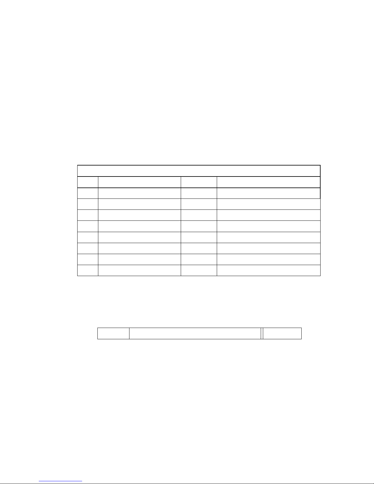
1-4. Composition
PN2
CPU
SH3 133M
VIDEO
S1D13806
S-RAM
512Kbyte
SDRAM
32Mbyte
F-EP ROM
4Mbyte
USB
PN10 PN16
CONTROL
PN5
PN4
PN15
PN12
PN9
S
W
LCD
Other
Ext Power
PN14 PN7
Touch Panel
Speaker
PN17 PN13 PN11 PN18 PN19
COM1 COM2
COM0
Expansion
terminal
LAN USB
Ether-net
LAN91C11
PN1
CF
Optional
Page 6
-4-
2. I/O
I/O in the board is composed with built-in I/O in CPU and I/O added outside.
Even if a sub-board does not exist when initializing, the movement for initializing is executed
to IC's installed in the sub-board.
In the manual, it is explained on CPU board only.
CPU has DMA function, but it cannot be used on the board.
The circuit of LCA chip is not published.
Here, I/O's are explained except I/O built-in SH-3.
Please refer to SH-3 hardware manual on I/O built-in SH-3.
2-1. Memory, I/O map
Regarding I/O, the memory mapped I/O is adopted, and the allocation is as follows:
Physical mapping on area
Area Address Bus width
Area 0 H'00000000 to H'03FFFFFF 16 F-EPROM 4M Byte to H'003FFFFF
Area 1 H'04000000 to H'07FFFFFF I/O built-in CPU
Area 2 H'08000000 to H'0BFFFFFF 32 S-DRAM, spare, unpopulated
Area 3 H'0C000000 to H'0FFFFFFF 32 S-DRAM, 32M, populated
Area 4 H'10000000 to H'13FFFFFF 16 I/O area
Area 5 H'14000000 to H'17FFFFFF 16 S-RAM 512K Byte
Area 6 H'18000000 to H'19FFFFFF 16 Used in CF
Area 7 H'1C000000 to H'1FFFFFFF Reserved
Above mapping can be traced on bigger number addresses.
Therefore, if you operate memory directly through OS, use the image in the range.
Please designate the address offset in which the absolute address can be
designated in case you adopt OS to use MMU such as LINUX.
Example: LINUX
Area 4 H'B0000000 to H'B3FFFFFF I/O area
Page 7

-5-
2-2. Detailed I/O area
Address
0x10000000 to 0x10000100 Multi-purpose I/O (LCA)
0x11000000 to 0x111FFFFF USB controller NOTE 1
0x12000000 to0x121FFFFF Video controller
0x12200000 to 0x1233FFFF Video memory (effective for 1280K byte)
0x13000000 to 0x132FFFFF LAN controller
(NOTE 1) Consecutive addresses are not used on IC accessing in 8-bit unit.
In case of accessing to a register, access to even numbered addresses.
/Although inside information on multipurpose I/O is not published, control necessary to
use this board is supplied in the library.
/On controller IC, please ask information to the manufacturers.
USB controller: CYPRESS SL811HST
Video controller: EPSON S1D13806F00A1
LAN controller: SMSC LAN91C111
2-3. IRQ
Outside IRQ of SH3-CPU is used.
IRQ mode, used in negative logic.
IRQ # Used controller
/IRQ 0 LAN controller
/IRQ 1 USB controller
/IRQ 2 Compact flash
/IRQ 3 Reserved
/IRQ 4 Reserved
Page 8

-6-
2-4. I/O built-in CPU
I/O’s built-in SH3-CPU are connected with the following terminals:
Function CPU terminal Connecter(s)
COM 0 RXD0 TXD0 PN11
COM 1 RXD2 TXD2 CTS2 RTS2 PN17 PN18
COM 2 RXD1 TXD1 PN13 PN19
Speaker DA0 PN7
HUDI
TCK /TRST TD0 /ASEBREAK TMS
TDI /ASEM0 /RESET PN9
AD AD0 AD1 AD2 AD3 PN14
Page 9

-7-
3. I/O terminals
PN1 Compact flash connector (/dev/had)
# Signal Function Direction # Signal Function Direction
1 GND Signal GND 26 CD1 Detect I
2 D3 Data bus I/O 27 D11 Data bus I/O
3 D4 Data bus I/O 28 D12 Data bus I/O
4 D5 Data bus I/O 29 D13 Data bus I/O
5 D6 Data bus I/O 30 D14 Data bus I/O
6 D7 Data bus I/O 31 D15 Data bus I/O
7 CE1 Selection signal 32 CE2 Selection signal
8 A10 Address bus O 33 NC Not used
9 OE Memory read 34 IORD I/O read signal
10 A9 Address bus O 35 IOWR I/O write signal
11 A8 Address bus O 36 WR Memory write
12 A7 Address bus O 37 RDY WAIT indication I
13 VCC VCC 3.3V 38 VCC VCC 3.3V
14 A6 Address bus O 39 CSEL Selection signal
15 A5 Address bus O 40 NC Not used
16 A4 Address bus O 41 RESET Reset
17 A3 Address bus O 42 NC Not used
18 A2 Address bus O 43 NC Not used
19 A1 Address bus O 44 REG Attribute selection
20 A0 Address bus O 45 BVD2 Not used
21 D0 Data bus I/O 46 BVD1 Not used
22 D1 Data bus I/O 47 D8 Data bus I/O
23 D2 Data bus I/O 48 D9 Data bus I/O
24 WP Protect O 49 D10 Data bus I/O
25 CD2 Detect I 50 GND Signal GND
Page 10

-8-
PN2 Expansion connector
# Signal Function # Signal Function
A1 GND Signal GND B1 GND Signal GND
A2 GND Signal GND B2 GND Signal GND
A3 VCC_5 VCC5V B3 VCC_5 VCC5V
A4 VCC_5 VCC5V B4 VCC_5 VCC5V
A5 VCC_3.3 VCC3.3V B5 CADD0 Address bus O
A6 VCC_3.3 VCC3.3V B6 CADD1 Address bus O
A7 VCC_3.3 VCC3.3V B7 GND Signal GND
A8 VCC_3.3 VCC3.3V B8 CADD2 Address bus O
A9 CADD16 Address bus O B9 CADD3 Address bus O
A10 CADD17 Address bus O B10 CADD4 Address bus O
A11 CADD18 Address bus O B11 CADD5 Address bus O
A12 CADD19 Address bus O B12 CADD6 Address bus O
A13 CADD20 Address bus O B13 CADD7 Address bus O
A14 CADD21 Address bus O B14 CADD8 Address bus O
A15 CADD22 Address bus O B15 CADD9 Address bus O
A16 CADD23 Address bus O B16 CADD10 Address bus O
A17 CADD24 Address bus O B17 CADD11 Address bus O
A18 CADD25 Address bus O B18 CADD12 Address bus O
A19 WR0 Write signal 0 O B19 CADD13 Address bus O
A20 WR1 Write signal 1 O B20 CADD14 Address bus O
A21 WR2 Write signal 2 O B21 CADD15 Address bus O
A22 WR3 Write signal 3 O B22 MAINCLK2 Clock O
A23 RD Read signal O B23 WR Write signal 0 O
A24 BS O B24 NC
A25 GND Signal GND B25 GND Signal GND
A26 CDA8 Data bus I/O B26 CDAT0 Data bus I/O
A27 CDA9 Data bus I/O B27 CDAT1 Data bus I/O
A28 CDA10 Data bus I/O B28 CDAT2 Data bus I/O
A29 CDA11 Data bus I/O B29 CDAT3 Data bus I/O
A30 CDA12 Data bus I/O B30 CDAT4 Data bus I/O
A31 CDA13 Data bus I/O B31 CDAT5 Data bus I/O
A32 CDA14 Data bus I/O B32 CDAT6 Data bus I/O
A33 CDA15 Data bus I/O B33 CDAT7 Data bus I/O
A34 IRQSUB0 IRQ0 IB34 CS0 Reserved O
Page 11

-9-
A35 IRQSUB1 IRQ 1 I B35 NC Reserved
A36 IRQ5 IRQ 5 I B36 CS2 Reserved O
A37 IRQ6 IRQ 6 I B37 DREQ0 DMA (Do not use) I
A38 IRQ7 IRQ 7 I B38 DREQ1 DMA (Do not use) I
A39 HRES Reset output I B39 DRAK1 DMA (Do not use) O
A40 NC B40 DRAK0 DMA (Do not use) O
A41 NC B41 NC
A42 RD Read O B42 NC
A43 IOSELSEL SUB board selection O B43 ANAD0 Analog input 0 I
A44 NC B44 ANAD1 Analog input 0 I
A45 DACK0 DMA (Do not use) O B45 INI_RD Reserved I
A46 DACK1 DMA (Do not use) O B46 INI_G Reserved I
A47 RESET Reset input I B47 INI_CE Reserved I
A48 WAIT Wait B48 INI_WR Reserved I
A49 GND Signal GND B49 GND Signal GND
A50 GND Signal GND B50 GND Signal GND
PN3 Terminals used by manufacturer (Do not use)
# Signal Function # Signal Function
1 TCK Clock I 2 GND Signal GND
3 TDO Data output O 4 VCC_3.3 VCC 3.3V
5 TMS Mode select I 6 VCC_3.3 VCC 3.3V
7 NC Not connected 8 NC Not connected
9 TDI Data input I 10 HRES Reset request I
PN4 Power terminal
# Signal Function
1 VCC_5 5v power source
2 GND Signal GND
3 GND Signal GND
4 24V
24v power source
(Not connected OK)
PN5 Drawer output
# Signal Function
1 24v Power source output O
2 OCGND Open collector GND output O
Page 12

-10-
PN6 Reset input
# Signal Function
1 /RESET Open collector /RESET I
PN7 Audio output ( /dev/da0 )
# Signal Function
1 SIGNAL Audio output O
2 GND Signal GND
PN9 JTAG I/F for debugging
# Signal Function # Signal Function
1 TCK Clock I 2 GND Signal GND
3 TRST H-UDI reset I 4 GND Signal GND
5 TDO Data output O 6 GND Signal GND
7 ASEBRKAK Emulator terminal O 8 NC Not connected
9 TMS Mode select I 10 GND Signal GND
11 TDI Data input I 12 GND Signal GND
13 CPURESET HUDI reset O 14 ASEMD0 ASE mode select I
Page 13

-11-
PN10 LCD output
# Signal Function # Signal Function
1 GND Signal GND 2 sift Shift clock O
3 line Line clock O 4 flame Frame clock O
5 GND Signal GND O 6 FPDAT17 Signal line O
7 FPDAT10 Signal line O 8 FPDAT9 Signal line O
9 FPDAT2 Signal line O 10 FPDAT1 Signal line O
11 FPDAT0 Signal line O 12 GND Signal GND O
13 FPDAT13 Signal line O 14 FPDAT12 Signal line O
15 FPDAT11 Signal line O 16 FPDAT5 Signal line O
17 FPDAT4 Signal line O 18 FPDAT3 Signal line O
19 GND Signal GND O 20 FPDAT16 Signal line O
21 FPDAT15 Signal line O 22 FPDAT14 Signal line O
23 FPDAT8 Signal line O 24 FPDAT7 Signal line O
25 FPDAT6 Signal line O 26 GND Signal GND
27 cont Panel control O 28 vcc LCD power source 3.3V
29 vcc LCD power source 3.3V 30 NC Not connected
31 NC Not connected xx NC Not connected
Page 14

-12-
PN11 POS keyboard connector ( /dev/ttySC0 )
# Signal Function
1 VCC_3.3 VCC 3.3V
2 RXD0 Receive data(TTL3.3v) I
3 TXD0 Transmit data(TTL3.3v) O
4 GND Signal GND
PN12 USB terminal
# Signal Function
1 VCC VCC5V
2 DATA+ Signal line I/O
3 DATA- Signal line I/O
4 GND Signal GND
PN13 POS customer display connector (/dev/ttySC2)
# Signal Function
1 VCC_5 VCC5V
2 TxD Transmit data O
3 GND Signal GND
PN14 Touch panel IF
# Signal Function
1 TPYD Y sensor - I
2 PPYD Y direction - O
3 PPYP Y direction + O
4 TPYU Y sensor+ I
5 TPXR Y sensor+ I
6 TPXL Y sensor- I
7 PPXP X direction + O
8 PPXD X direction - O
Page 15

-13-
PN15 Expansion connector 2
# Signal Function # Signal Function
1 GND Signal GND 2 CD1 Detect I
3 D3 Data bus I/O 4D11 Data bus I/O
5 D4 Data bus I/O 6 D12 Data bus I/O
7 D5 Data bus I/O 8 D13 Data bus I/O
9 D6 Data bus I/O 10 D14 Data bus I/O
11 D7 Data bus I/O 12 D15 Data bus I/O
13 CE1 Selection signal 14 CE2 Selection signal O
15 A10 Address bus O 16 NC Not used
17 OE Memory read 18 IORD IO read signal O
19 A9 Address bus O 20 IOWR IO write signal O
21 A8 Address bus O 22 WR Memory write O
23 A7 Address bus O 24 RDY WAIT indication I
25 VCC VCC3.3V 26 VCC VCC3.3V
27 A6 Address bus O 28 CSEL Selection signal O
29 A5 Address bus O 30 NC Not used
31 A4 Address bus O 32 RESET Reset O
33 A3 Address bus O 34 NC Not used
35 A2 Address bus O 36 NC Not used
37 A1 Address bus O 38 REG Attribute selection O
39 A0 Address bus O 40 BVD2 Not used
41 D0 Data bus I/O 42 BVD1 Not used
43 D1 Data bus I/O 44 D8 Data bus I/O
45 D2 Data bus I/O 46 D9 Data bus I/O
47 WP Protect O 48 D10 Data bus I/O
49 CD2 Detect I 50 GND Signal GND
Page 16

-14-
PN16 10/100 BASE-T LAN terminal ( /dev/eth0 )
# Signal Function
1 TX+ Sending + O
2 TX- Sending - O
3 RD+ Receiving + I
4 GND Signal GND
5 GND Signal GND
6 RX- Receiving- I
7 GND Signal GND
8 GND Signal GND
PN17 Standard input/output serial connector (/dev/ttySC1)
# Signal Function # Signal Function
1 DCD Data terminal ready (Not used) I 6 DSR Data set ready (Not used) I
2 RxD Receive data I 7 RTS Request to send O
3 TxD Transmit data O 8 CTS Clear to send I
4 DTR Data terminal ready O 9 RI Ring indicator (Not used) I
5 GND Signal GND
PN18
Serial connector (/dev/ttySC1) Mutually exclusive use with PIN17 PIN # differs to
usual.
# Signal Function #
Sign
al
Function
1 DCD Data terminal ready (Not used) I 6 DSR Data set ready (Not used) I
2 RxD Receive data I 7 RTS Request to send O
3 TxD Transmit data O 8 CTS Clear to send I
4 DTR Data terminal ready O 9 RI Ring indicator (Not used) I
5 GND Signal GND 10 NC Not connected
Page 17

-15-
PN19
Serial connector (/dev/ttySC2) Mutually exclusive use with PIN13
PIN # differs to usual.
#
Sign
al
Function #
Sign
al
Function
1 DCD Data terminal ready (Not used) I 6 DSR Data set ready (Not used) I
2 RxD Receive data I 7 RTS Request to send O
3 TxD Transmit data O 8 CTS Clear to send I
4 DTR Data terminal ready O 9 RI Ring indicator (Not used) I
5 GND Signal GND 10 NC Not connected
NOTE: PN22, PN23, and PN24 must not be used.
Page 18

-16-
4. LAN-LED display
IC12 Display of LED is programmed as follows:
LAN-LED Color Function
Upper Green Power supply indication: Lighting when 5V power is supplied.
Middle Red LAN: Built up the link at 100MBps or 10MBps.
Lower Red LAN: Packet sent or received
Page 19

-17-
Inquiry
TOWA MECCS CORPORATION
Market development headquarters
Corporation marketing Dept
Persons in charge:Masuda and Sasaoka
TEL:81-3-3816-7864
E-mail:info@towa-meccs.co.jp
We renew detailed information in our home page from time to time.
■ SH Board TMM1000
http://www.towanet.com/seihin/sh_board/index.html
■ TOWA MECCS CORPORATION
http://www.towa-meccs.co.jp
 Loading...