


ASSEMBLY and USER MANUAL
500 Series
Suite 5, Fairfield, 1048 Govan Road, Glasgow G51 4XS, United Kingdom.
info@totalaudiocontrol.com www.totalaudiocontrol.com

2
INTRODUCTION
Thank you for purchasing MICPRE TWO in kit form. You will have a lot of fun in building and using it.
MICPRE TWO is the second in our flagship “Designed by Langley” series of microphone pre-amplifiers.
MICPRE TWO follows the topology of the transformerless microphone preamplifier employed on the Amek Rembrandt console, with
the use of dual ganged potentiometer arrangement to provide greater linearity of the gain control, compared with the use of a single
ganged potentiometer. This was derived from the Amek Angela and the M2500 console preamplifiers. MICPRE TWO provides
exceptional noise performance even at low gain settings.
A high impedance balanced instrument input is provided, accessed by a front panel jack socket. Provision is also made for connection
to MID-SIDE ONE M-S Encoder/Decoder and an output splitter in 1U 19” rack configuration. Gain is continuously variable from 0dB
to 66dB. A PHASE reversal switch and a -15dB PAD switch are provided. A meter measures the signal output from an internal source.
Typical specifications:
Mic. input impedance : >5k ohms, PAD IN >4.5k ohms.
Instrument input impedance : 1.5M ohms
Frequency response : +/- 0.5dB, 20Hz-80 kHz (up to 60dB gain).
Phase response (EQ out) : +/-30 deg., 20Hz-80 kHz (up to 60dBgain).
Mic input maximum input level : +21dBu (+28dBu with pad)
Maximum output (into 100k ohms) : +26dBu
THD&N (+10dBu input signal) : better than 0.05%, 20Hz-20 kHz (up to 60dB gain).
Mic. EIN : 22Hz-22 kHz, RMS, 150 ohm source: -127.5dBu.
Minimum gain output noise : 22Hz-22 kHz, RMS, 150 ohm source: -99dBu.
Output impedance : 75 ohms
3
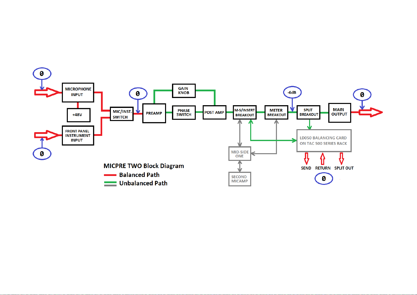
Figure 1: Block Diagram.
ALL SPECIFICATIONS ARE SUBJECT TO CHANGE.

4
FEW WORDS ON ASSEMBLY
Before rushing into building your MICPRE TWO you should study this manual from front to back, and familiarise yourself with the
design before starting to solder the first component. As the expression says “one picture tells a thousand words”.
The components are packed and numbered in the correct order. The numbers correspond to the bill of materials. Open them one at
a time. Do not open the next package before completing the assembly of the previous one. There is a reason behind each stage.
Populating a PCB always starts with the smallest components. Resistors and/or small signal diodes being the first. If you solder the
larger components first you’ll have a hard time in soldering the resistors or the small signal diodes.
Before soldering a component visually check its value and designation. Although normally it is not required, testing them would also
be a good practice (excluding integrated circuits) before they go on the board. We are extremely lucky to be living at a time when a
reasonably well performing digital multimeter with semiconductor testing capability, or a capacitance meter can be picked up from
e-bay for the cost of literally a burger meal. Therefore, investing into a few handheld meters would pay dividends in the long run.
A good quality soldering iron with a fine tip and a set of hand tools are a must. Plumber’s torch does not have a place in electronics
assembly and component leads are not trimmed using a Black Smith’s pliers. A miniature close cutting side cutter will have to be a
part of your tool kit. Equally fixing an M2 screw will not be possible with a screw driver normally used for M10 bolt. A simple spring
action desoldering pump will do fine for single sided boards. But for double sided/plated through boards, such as this a proper
(electric motor pump action) de-soldering tool will be essential. However, you do not have to get the ones that require remortgaging your house. There are affordable ones that will also do a good job.
Most faults will arise due to incorrect components being inserted or solder bridges. It is particularly important to closely examine
the soldering of components with close pads such as transistors. Therefore, unless you have eagle eyes, checking each solder node
with a hand held or table mount magnifier as you go along will be an extremely good practice.

5
Do not stay on the components with the soldering iron for too long as there can be a possibility of causing damage. You should be
able to get in and out of a solder node within few seconds.
There is no need to crop connectors, potentiometers or switches unless specified.
Safety first, be extremely careful when trimming component leads as these can easily fly off into your face. Always hold the lead with
one hand while trimming it with the other.
In general do not rush. Work methodically and have fun.
Total Audio Control
SEPTEMBER 2019
6
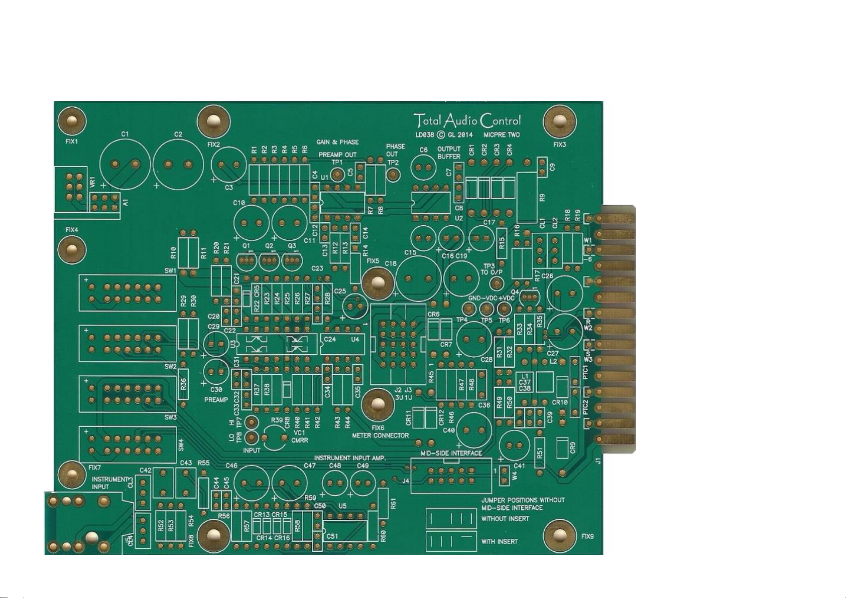
LDO38 MAIN BOARD (ZOOM IN TO ENLARGE)
7
COMPONENT DESIGNATIONS WITH VALUES

8
LD038 MAIN BOARD ASSEMBLY.
Make sure that the polarity notches on both the IC sockets and 10 way box headers match the
silk screen on the main board.
9
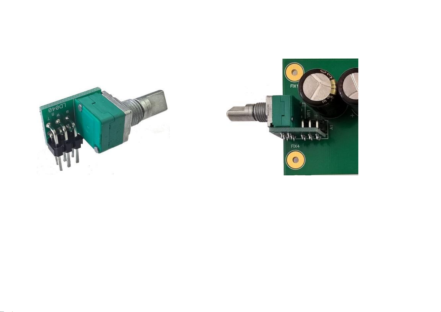
LD040 GAIN POTENTIOMETER ADAPTER CARD ASSEMBLY.
1). Solder the 6-pin right angle connector to the PCB paying particular attention to the position of the plastic
spacer. This should butt up against the LD040.
2). Solder the gain potentiometer.
3). Insert LD040 Gain Potentiometer Adapter card into the main board.
DO NOT SOLDER THE LD040 ADAPTER CARD ASSEMBLY TO THE MAIN BOARD YET.
10
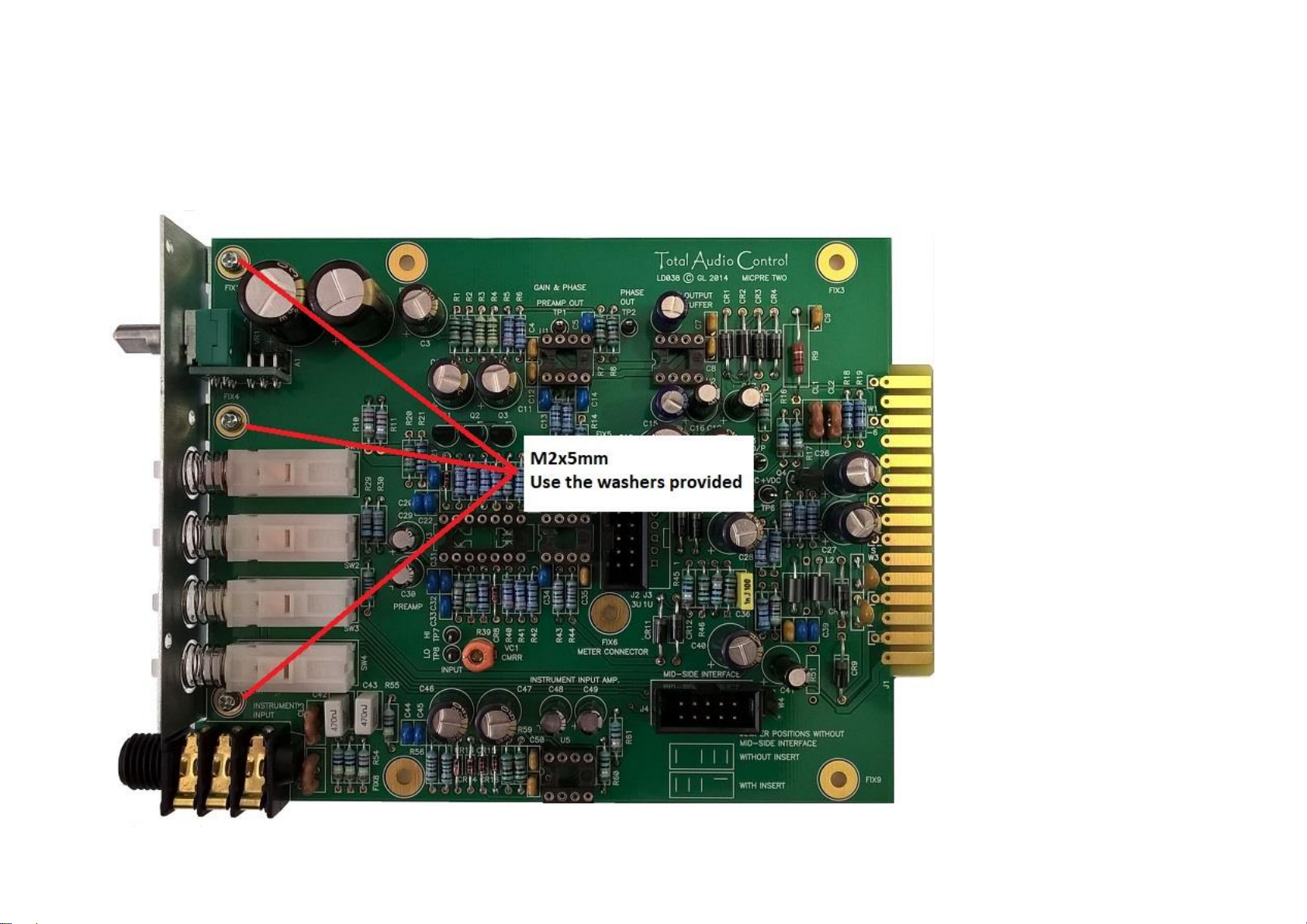
BACKPLATE ASSEMBLY
1).Gently fit the back plate over the potentiometer. The back plate sits on the component side of the PCB.
Fix it using three M2 screws from the solder side of the main PCB.
11
2). Fix the potentiometer onto the back plate by using the nut/washer. Do not apply excessive force.
4). Now solder the LD040 gain potentiometer adapter card onto the main board.

12
HEX PILLARS
Fit M3 x 23mm hex pillars into FIX 5 and FIX 6 holes using M3 x 5mm screws with shake proof washers from the
solder side of the main board.

13
FACEPLATE ASSEMBLY.
Fix the Faceplate to the backplate using three M3 screws. Use the extra anti vibration/locking washers
In addition to the ones already on the screw. This is to slightly shorten the length of the screws.

14
LEFT HAND SIDE SCREEN PLATE ASSEMBLY.
Fit LHS screen plate through Fix2, Fix3, Fix8 and Fix9 using M3 screws.

15
LD037 8 LED METER ASSEMBLY:

16
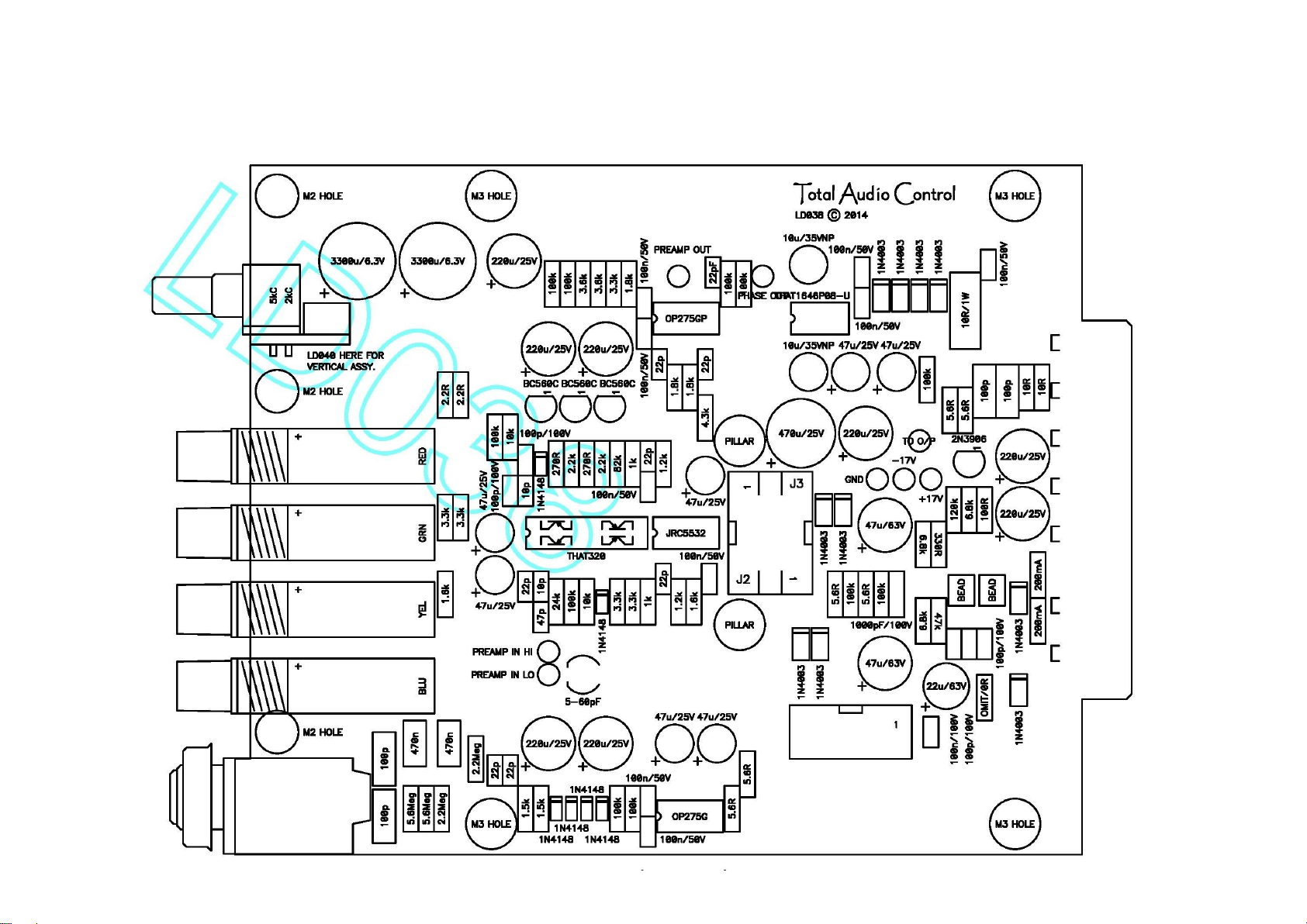
COMPONENT DESIGNATIONS WITH VALUES

17
FITTING OF METER LEDs:
The cathode is the short lead. Trim the cathode to 10mm (0.4").
A "C" on the silkscreen indicates the cathode position.
Using the faceplate as a jig align the LEDs with the trimmed cathodes on the component side of the PCB.
Tack-solder the LEDs as far as from the plastic body as possible.
Trim the anode leads to 10mm and solder to the pads (on the solder side of the PCB).
DO NOT APPLY HEAT FOR MORE THAN A FEW SECONDS OTHERWISE THE LEDs MAY BE DAMAGED.

18

19

20
VISUAL CHECK:
Check that ICs are inserted the right way round.
Check all joints are properly soldered.
Check that the leads are properly cropped using close cutting side cutters.
There is no need to crop connectors, potentiometers or switches unless specified.
Most faults will arise due to incorrect components being inserted or solder bridges.
It is important to closely examine the soldering on components with close pads such as transistors.
Fit jumper links on J4 for a basic setup without insert points. (DO NOT fit jumper on the 2 way header W4.)

21
APPLYING POWER
After switching the module on do the following checks:
Do all the illuminated switches light up?
Does the meter read? – It might initially but the bar should stabilise with no LEDs illuminated.
Does anything smell of burning or feel excessively warm. If so switch off. Wait a short time then try to locate it.
INITIAL MEASUREMENTS
If all seems well, using a DC voltmeter measure each of the test points with reference to ground:
TP1: at minimum gain -2.57mV, at maximum gain -2.57mV Preamp Out
TP2: at minimum gain -2.57mV, at maximum gain -2.66mV Phase Out
TP3 0V To Output
TP4 0V GND
TP5 -16V -VDC
TP6 +16V +VDC
TP7: at minimum gain +160mV, at maximum gain +160mV Input Hi
TP8: at minimum gain +160mV, at maximum gain +160mV Input Lo
If it is possible to measure the supply rail currents they should be as follows with no input signals:
61mA on the positive rail and 54mA on the negative rail.
Worst case: +16dB into instrument input and +26dBu output into 600R load (this uses all op-amps at maximum drive and does
not change with frequency in the audio band): Positive rail = 89mA, negative = 82mA
The higher current on the positive rail is mainly due to the voltage reference for the meter.
All these figures are nominal, but large deviations may indicate a fault.

22
SIGNAL PATH TESTS
These tests should be carried out using balanced input and output signals.
Input signals should be from a low impedance source and the output load should be greater than 10k ohms.
Turn the gain control to 0dB.
Ensure that none of the illuminated switches are pressed
Connect a 1kHz signal of +4dBu (1.23V RMS) to the mic input.
The meter should read with all green LEDs illuminated.
A signal of approximately +4dBu should appear at the MAIN output.
Remove the signal from the mic input and apply a 1kHz signal of +4dB (1.23V RMS) to the instrument e input.
Press the INSTRUMENT switch.
The meter should read with all green LEDs illuminated.
A signal of approximately +4dBu should appear at the MAIN output.
Once these tests have been carried out it is known that the module basically works.
FURTHER SIGNAL PATH TESTS
These are best carried out with an audio source, microphone, instrument or recorded music, as appropriate.
Check the gain control over its whole range. Appropriate signal levels will have to be applied otherwise distortion will occur at
high gains.
Check the PAD switch. There should be a 15dB signal attenuation of both mic and instrument inputs when engaged.
Check the PHASE switch. There should be no level change when operated.
Check that the +48V phantom power switch operates.
Switches related to the changes on the input will cause clicks when activated, particularly at high gains. This is to be expected.

23
OUTPUT SYMMETRY:
Output symmetry is a measure of how much the device can suppress common-mode signals at its output.
No output symmetry trimming is necessary as the THAT output device is laser trimmed.
CMRR (COMMON MODE REJECTION RATIO):
The CMRR is a measure of how much the device can suppress common-mode signals at its input.
For best rejection performance the capacitors on each input leg should be the same (100pF). To meet this requirement as close
as possible the capacitors C20 and C31 are hand selected and closely matched. Therefore no CMRR trimming is required.

24
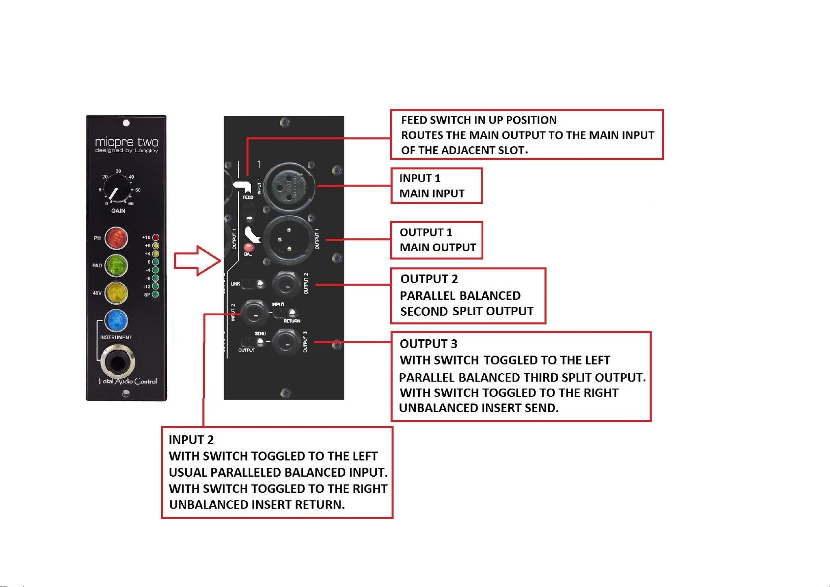
INSERT SEND/RETURN POINTS and AUXILIARY -6dB OUTPUT:
W1 (pin 3): -6dB Output
W2 (pin 7): Insert Return
W3 (pin 9): Insert Send
These points are unbalanced by nature and do not have links to the card edge connector as default. They are
linked depending on how the insert points at the rack interface with the outside world.
All of Total Audio Control 500 series racks fully support insert send/return. However, if your 500 series rack does
not support insert points, then you will require INSERT ONE module.

25
UNBALANCED INSERT OPERATION:
For unbalanced send/return connection LD039 ESD/EMC protection card must be installed. Making unbalanced
connections to these I/O paths without this card could result in damage to the module or external equipment.
Please note that LD039 ESD/EMC protection card is not part of MICPRE TWO kit and should be purchased
separately.

26
LD039 EMC/ESD CARD ASSEMBLY:

27
Components:
R1, R2, R3 : 10R
CR1, CR2, CR3, CR4, CR5, CR6 : 1N4003
CL1, CL2, CL3 : 100pF Filter Capacitor
J1, J2, J3, J4, J5, J6, J7 : 2 Way 2.54mm Pitch Header
Solder the resistors, diodes and capacitors. Do not solder the 2 way headers yet.

28
Insert the headers into the main board. DO NOT solder them yet.
Insert the LD039 board, align the headers in the centre of their respective pads and carefully solder them
from the bottom side.

29
Remove the assembly from the main module and solder the headers on the component side of the LD039.
Fit the LD039 assembly back onto the main card and solder in place.

30
BALANCED INSERT OPERATION
For balanced insert operation LD038 EMC/ESD CARD is not required. All you have to do is to link W1, W2 and
W3 using excess leads left over from resistors or capacitors.
However, balanced insert operation requires the use of LD050 BALANCING CARD which is installed into the
Total Audio Control 500 series rack.
Please also note that the LD050 BALANCING CARD is not part of the MICPRE TWO kit and should be purchased
separately.

31
CONFIGURING J4 TO ACTIVATE INSERT SEND/RETURN:
In this configuration;
Preamp output (pin 3) is routed to insert send (pin 1).
Insert return (pin 7) is routed to the input of the output (unbalanced to balanced line driver) stage
(pin 4, 8 & 10).
Meter input (pin 9) is jumpered to the input of the output stage (pin 10).
However, this naturally forms a serial processing. Therefore for the signal to reach the main output, and the
meter to be able to read, the insert send and return jacks at the rack will need to be patched.
32
UNBALANCED INSERT INTERFACING AT Total Audio Control 500 Series Racks:

33
BALANCED INSERT INTERFACING AT Total Audio Control 500 Series Racks:

34
FREQUENCY RESPONSE:
Measurements are carried out using Audio Precision APx520 with 150R source and 200k load.
The connection from the Apx520 to the module is via 160ft of Gotham microphone cable with
hot-to-cold signal capacitance of 4nF and signal to screen capacitance of 8nF.
Measurement bandwidth is 5Hz – 80kHz.
The Apx520 is set to 90kHz bandwidth, and no filters, with test settings as below:

35
AP PLOT 1:
FREQUENCY RESPONSE FOR EACH GAIN SETTING WITH A –50dBu INPUT.
There is LF roll off due to the gain control capacitor at high gain settings. It is -0.3dB @66dB gain and -0.1dB @ 60dB gain.

36
AP PLOT 2:
FREQUENCY RESPONSE AT HIGH GAIN SETTINGS WITH AND WITHOUT PAD:
At maximum gain –3dB points are at 5Hz and greater than 200kHz.
At 20Hz loss is approx.0.5dB and at 20kHz it is 0.2dB.
Reducing the gain by 6dB widens the LF bandwidth, but the HF bandwidth is largely determined by the input filter.
Lower input impedances will result in wider HF bandwidth and possibly also some lift at or above 300kHz.
Noise at unity gain (PAD not enabled) = -99.4dB (22Hz-22kHz RMS):

37
©Total Audio Control
 Loading...