

Total Audio Control 500 Series, Micpre One Assembly Manual
ASSEMBLY MANUAL
500 Series
17 Park Terrace Lane, Glasgow, G3 6BQ, United Kingdom
info@totalaudiocontrol.com www.totalaudiocontrol.com

2
INTRODUCTION
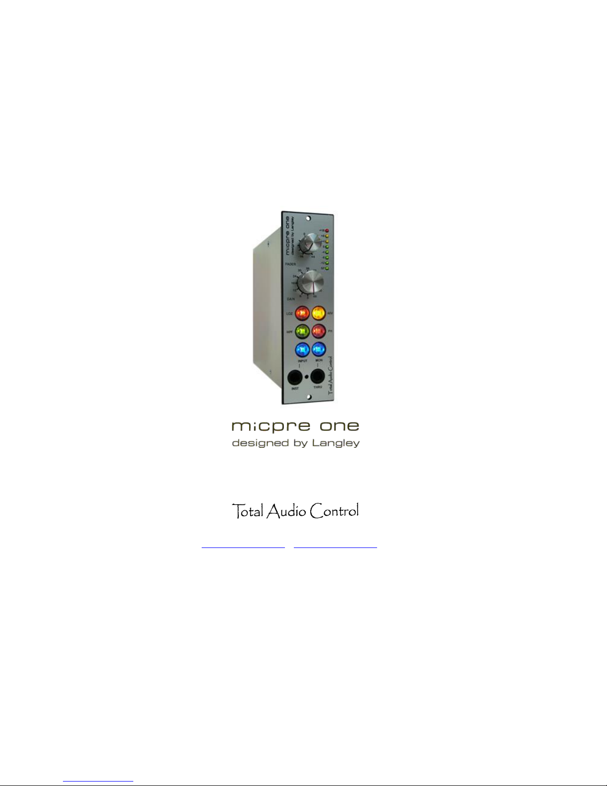
Thank you for purchasing MICPRE ONE in kit form. You will have a lot of fun in building and using it.
MICPRE ONE is one of the first in our flagship “Designed by Langley” series of pro-audio products. Yes, as the name reveals it is
designed by Mr Graham Langley, a name that requires no introduction. The premium quality components are used without any
exception to provide the highest performance and most reliable operational life. The PCBs are fully gold plated. Nothing is
compromised.
MICPRE ONE is similar in topology to the transformerless design Graham used on the Amek M2500 mixing console and the original
Angela console of 1982.
A number of improvements have been made, but the design retains the use of parallel matched transistors and constant current
sources. Exceptional noise performance has been achieved. Particularly at low gain settings. The signal path is balanced throughout.
0dB to 66dB of gain is selected in 6dB steps by a rotary switch and this is followed by the fader stage which provides an additional
4dB of gain and up to 24dB of control to adjust between switch settings and also to attenuate the final output to suit consumer
interface.
Switches are fitted for input impedance selection, a passive high pass filter before the preamplifier, phase and phantom power.
A high impedance balanced instrument input is also provided on a front panel jack.
An additional switch selects the source for a second front panel that can provide a balanced “THRU” output directly from the
instrument source, or monitor off the main path.
An 8 segment pre fader LED meter is provided. The Signal Present LED illuminates at -18dBu. The response of the main bar
approximates that of a PPM, while the +18 LED has faster attack and slower decay to catch peaks.
3
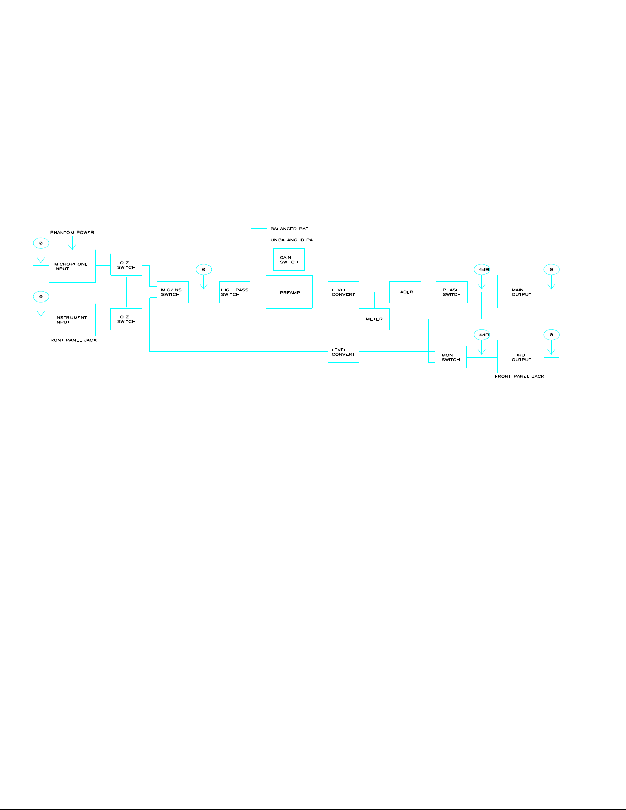
Figure 1: Block Diagram
Typical specification, both paths:
Mic. input impedance: switchable 5k ohms/600 ohms
Instrument input impedance: switchable 1.5M ohms/50k or 10k ohms
High pass filter: 120Hz @ 6dB/octave (nominal).
Frequency response: +/- 0.5dB, 20Hz-80kHz (up to 60dB gain).
Phase response (EQ out): +/-30 deg., 20Hz-80kHz (up to 60dBgain).
Maximum output (into 100k ohms) +27dBu
THD&N (+10dBu input signal): better than 0.05%, 20Hz-20kHz (up to 60dBgain).
Mic. EIN, 22Hz-22kHz, RMS, 150 ohm source: -128dBu.
Output impedance (main and THRU) 75 ohms
ALL SPECIFICATIONS ARE SUJECT TO CHANGE.

4
FEW WORDS ON ASSEMBLY
This manual is not meant to be a step by step guide for the assembly. Therefore, before rushing into building your MICPRE ONE you
should study it from front to back and familiarise yourself with the design before starting to solder the first component. As the
expression says “one picture tells a thousand words”.
The components are packed and numbered in the correct order. The numbers correspond to the bill of materials. Open them one at
a time. Do not open the next package before completing the assembly of the previous one. There is a reason behind each stage.
Populating a PCB always starts with the smallest components. Resistors and/or small signal diodes being the first. If you solder the
larger components first you’ll have a hard time in soldering the resistors or the small signal diodes.
Before soldering a component visually check its value and designation. Although normally it is not required, testing them would also
be a good practice (excluding integrated circuits) before they go on the board. We are extremely lucky to be living at a time when a
reasonably well performing digital multimeter with semiconductor testing capability or a capacitance meter can be picked up from ebay for the cost of literally a burger meal. Therefore, investing into a few handheld meters would pay dividends in the long run.
A good quality soldering iron with a fine tip and a set of hand tools are a must. Plumber’s torch does not have a place in electronics
assembly and component leads are not trimmed using a Black Smith’s pliers. A miniature close cutting side cutter will have to be a
part of your tool kit. Equally fixing an M2 screw will not be possible with a screw driver normally used for M10 bolt. A simple spring
action desoldering pump will do fine for single sided boards. But for double sided/plated through boards such as this a proper
(electric motor pump action) de-soldering tool will be essential. However, you do not have to get the ones that require remortgaging your house. There are affordable ones that will also do a good job.
Most faults will arise due to incorrect components being inserted or solder bridges. It is particularly important to closely examine
the soldering of components with close pads such as transistors. Therefore, unless you have eagle eyes, checking each solder node
with a hand held or table mount magnifier as you go along will be an extremely good practice.

5
Do not stay on the components with the soldering iron for too long as there can be a possibility of causing damage. You should be
able to get in and out of a solder node within few seconds.
There is no need to crop connectors, potentiometers or switches unless specified.
Safety first, Be extremely careful when trimming component leads as these can easily fly off into your face. Always hold the lead with
one hand while trimming it with the other.
In general do not rush. Work methodically and have fun.
Total Audio Control
March 2013
6
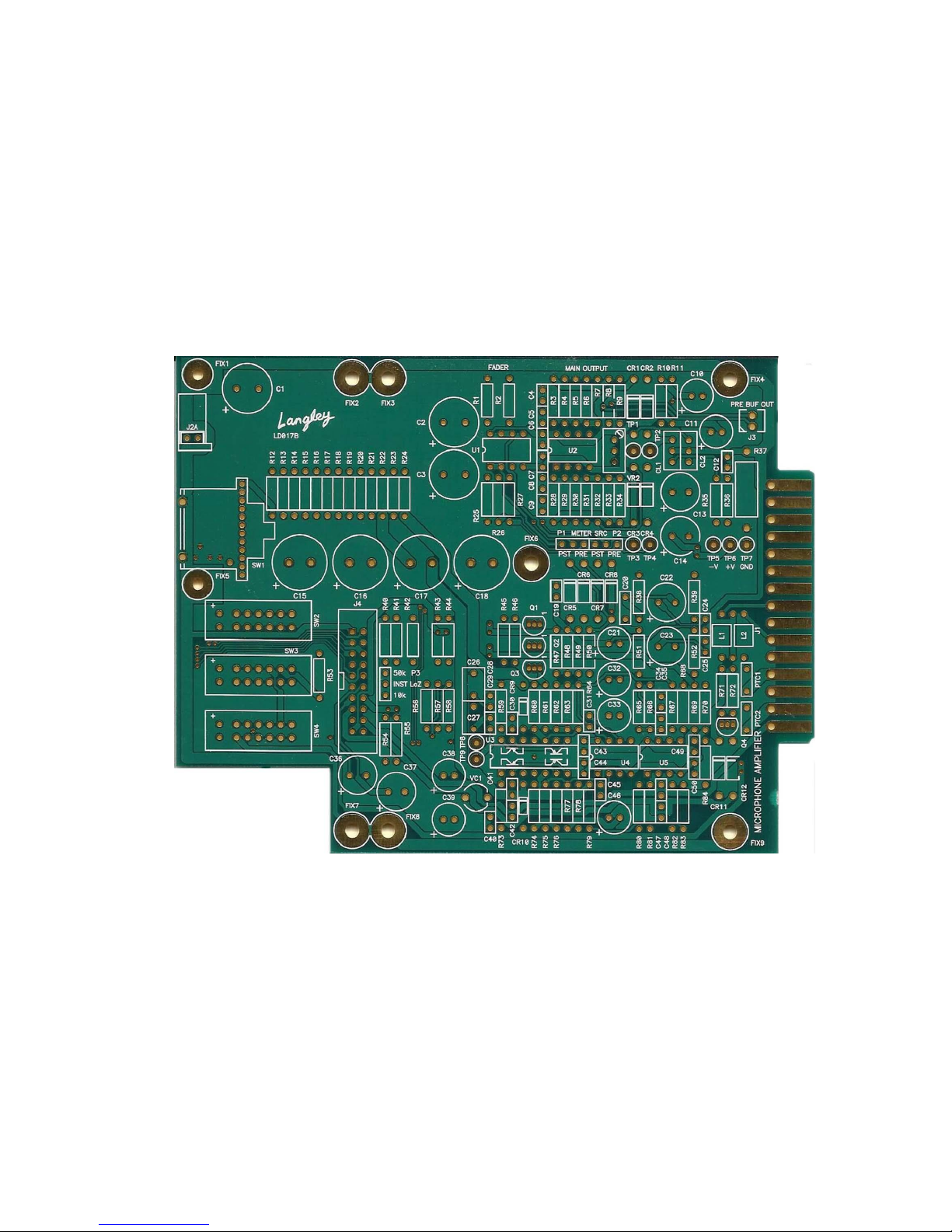
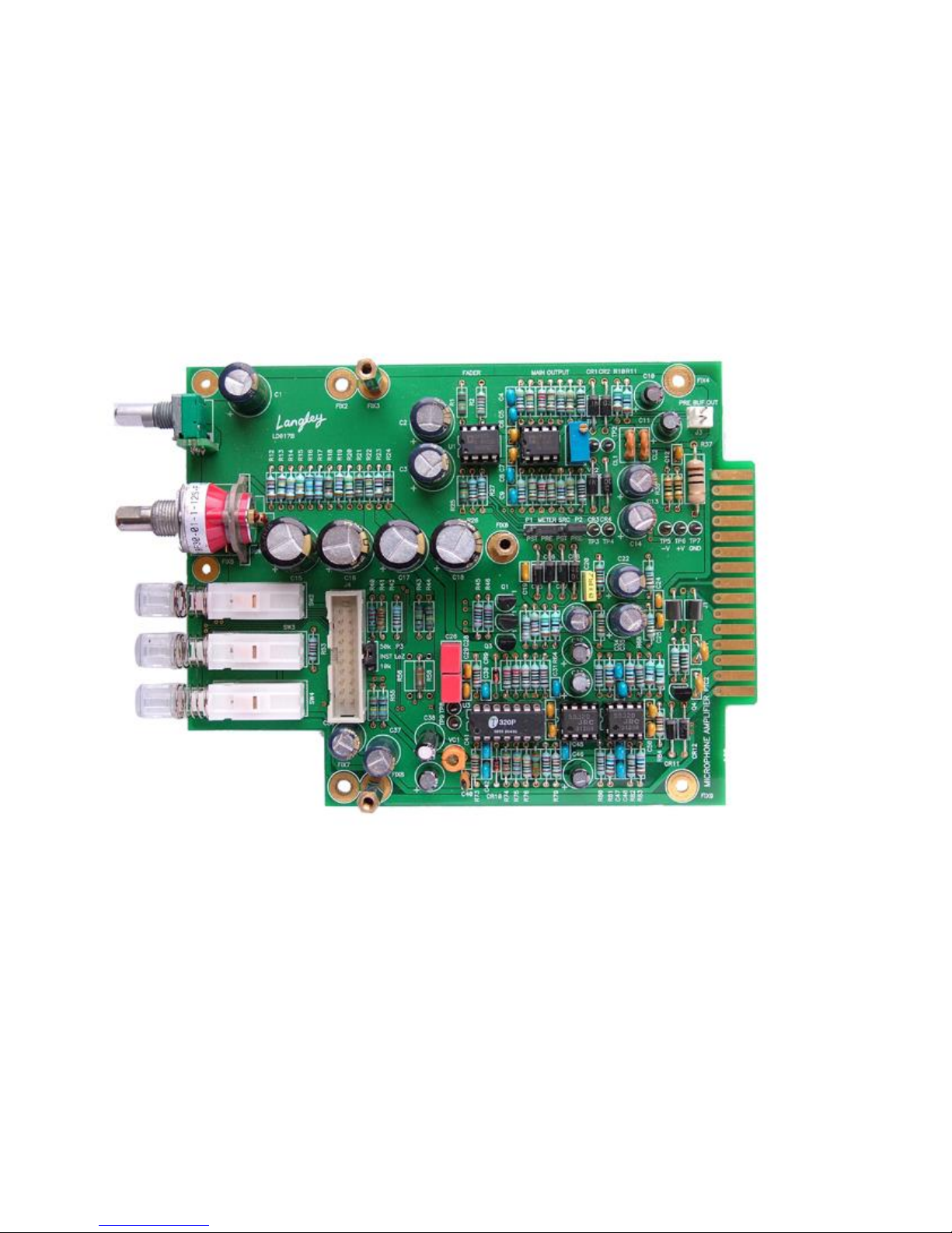
LDO17 B MAIN BOARD (ZOOM IN TO ENLARGE)
7
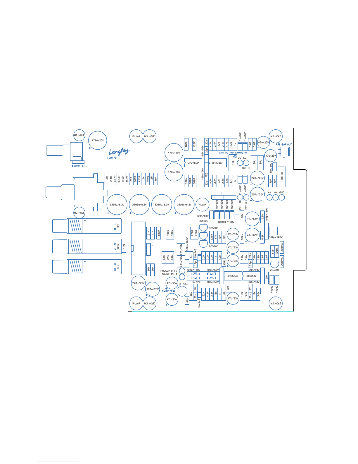
COMPONENT DESIGNATIONS WITH VALUES
8
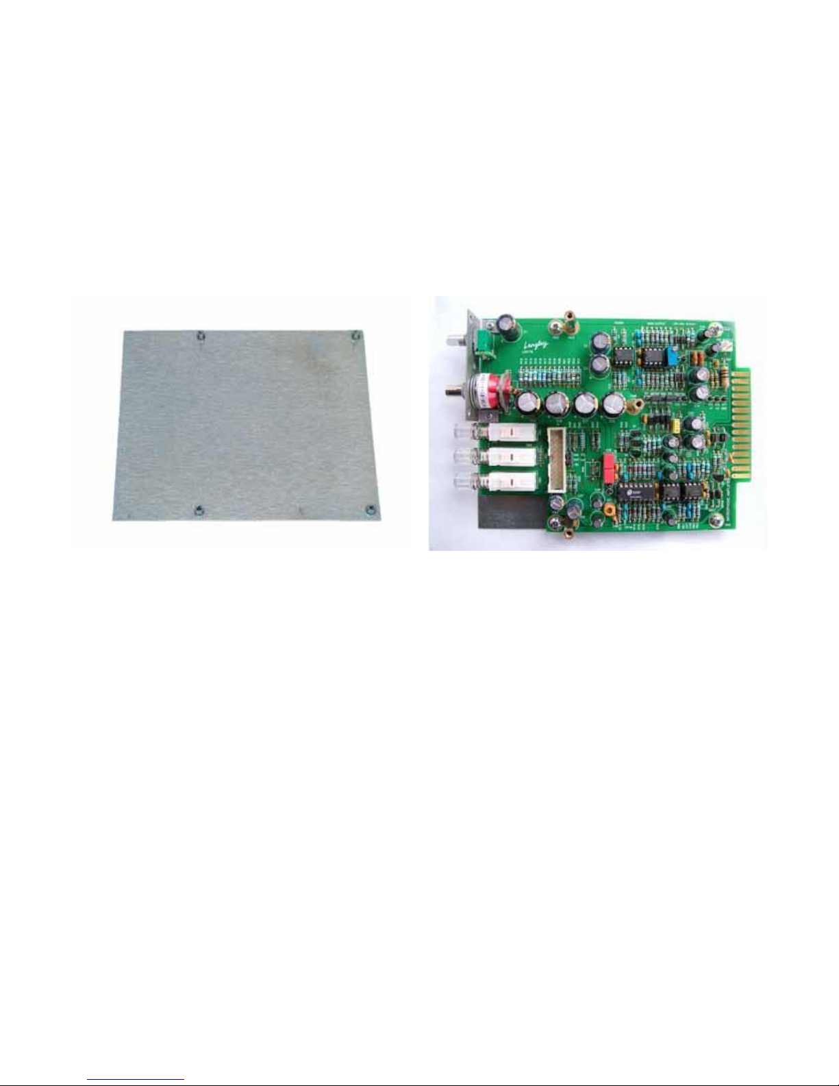
LD017B MAIN BOARD ASSEMBLED.
9
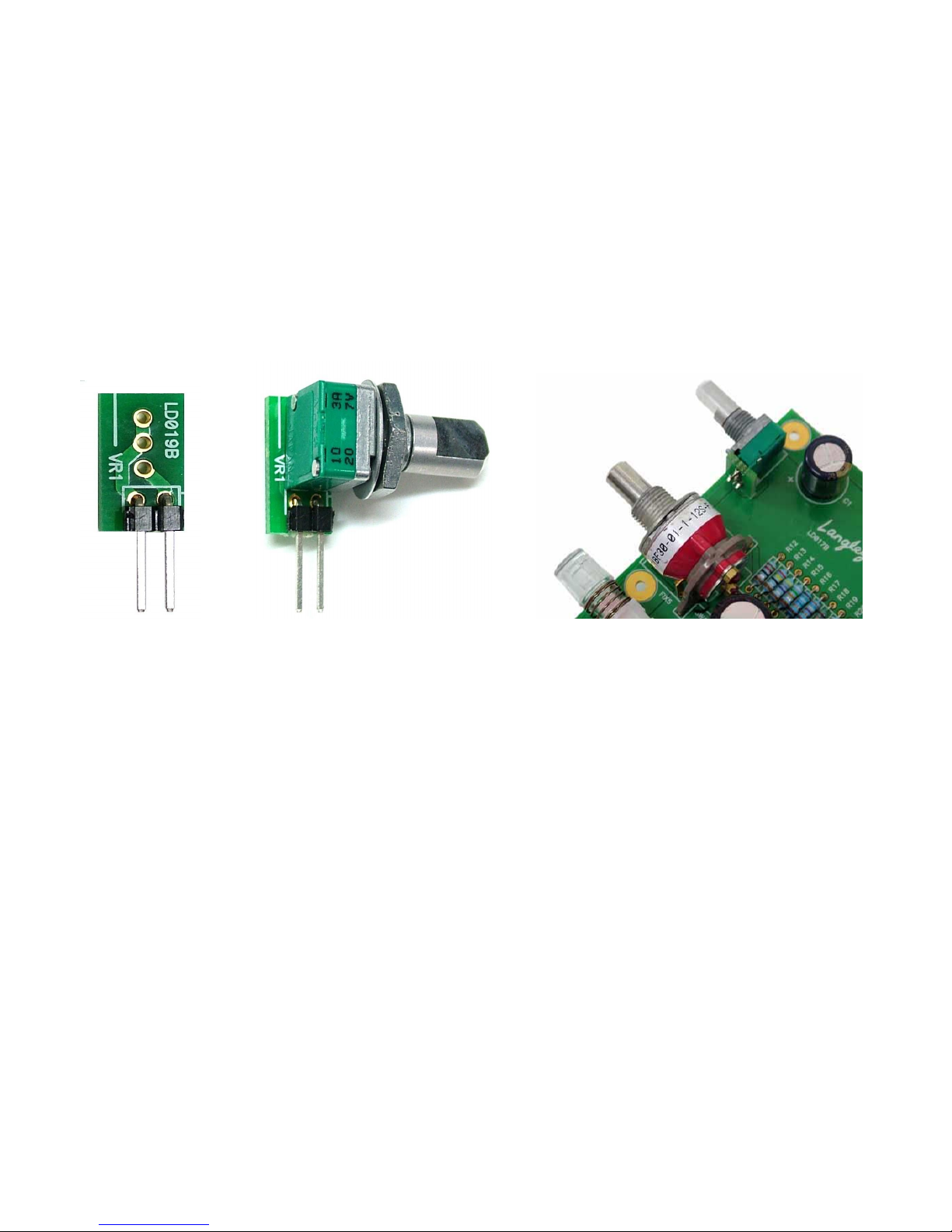
LD019B FADER ADAPTER CARD ASSEMBLY.
Solder the 2-pin right angle connector to the PCB paying particular attention to the position of the plastic
spacer. This should butt up against the LD017.
Solder the fader potentiometer.
DO NOT SOLDER THE LD019B FADER ADAPTER CARD ASSEMBLY TO THE MAIN BOARD YET.
10
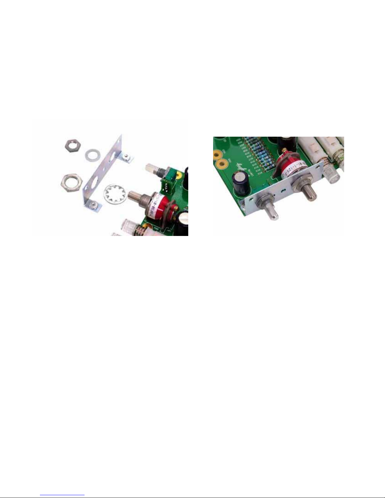
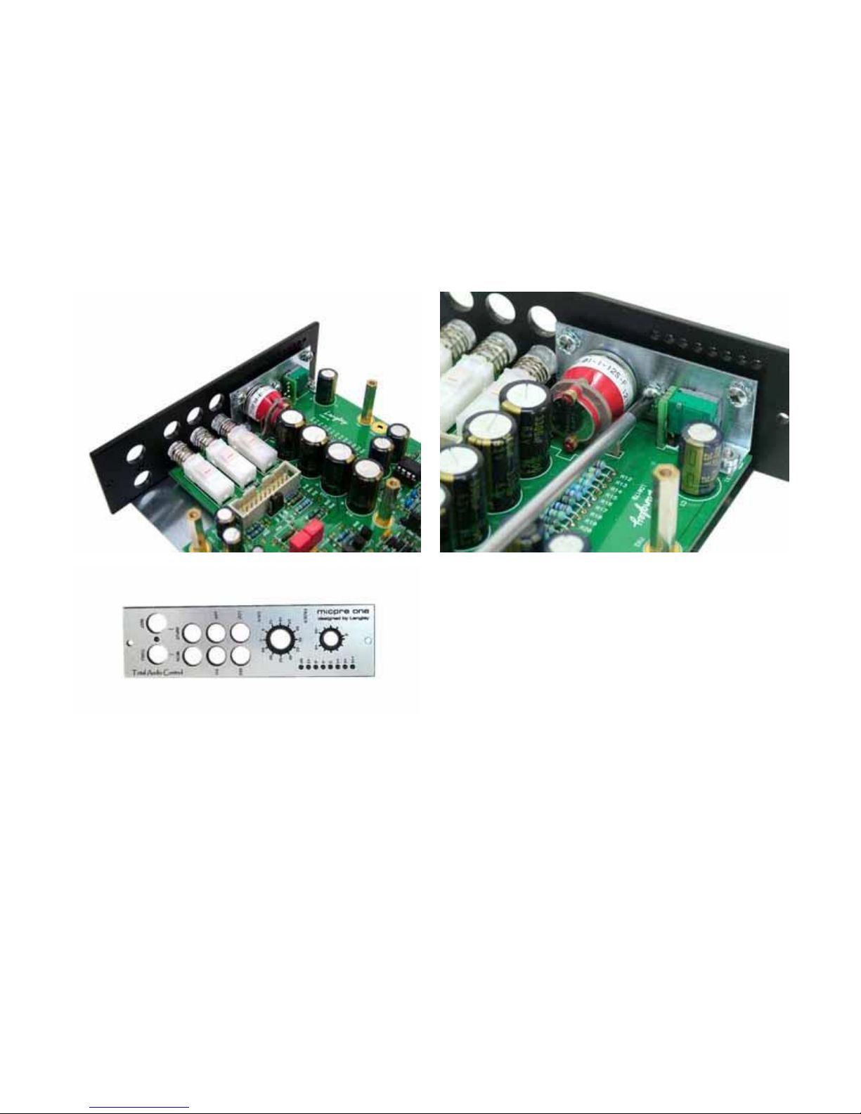
BACK PLATE ASSEMBLY.
1). Solder the Gain Switch onto the main board.
2). Place the anti-vibration (or locking) washer over the gain switch. This will act as a filler/spacer between the
gain switch and back plate.
3). Insert LD019B Fader Adapter card into the main board. Do not solder it yet.
4).Gently fit the back plate over the gain switch and the fader potentiometer. The back plate sits on the
component side of the PCB. Fix it using two M2 screws which are inserted from the solder side of the main PCB.
4). Fix the gain switch and the fader potentiometer onto the back plate by using their respective nuts/washer.
Do not apply excessive force.
5). Solder the LD019B Fader Adapter Card.
11
LEFT HAND SIDE SCREEN PLATE ASSEMBLY.
The LD017B main board is fixed through Fix2, Fix4, Fix7 and Fix9 using M3 screws.
Fix3 (top), Fix6 (middle) and Fix8 (bottom) are the hex pillars which are locked from the solder side using
washers/nuts.
12
FACE PLATE ASSEMBLY.
Fix the Face Plate to the Back Plate using three M3 screws. Use the two extra anti vibration/locking washers
In addition to the one already on the screw. This is to slightly shorten the length of the screws.
13
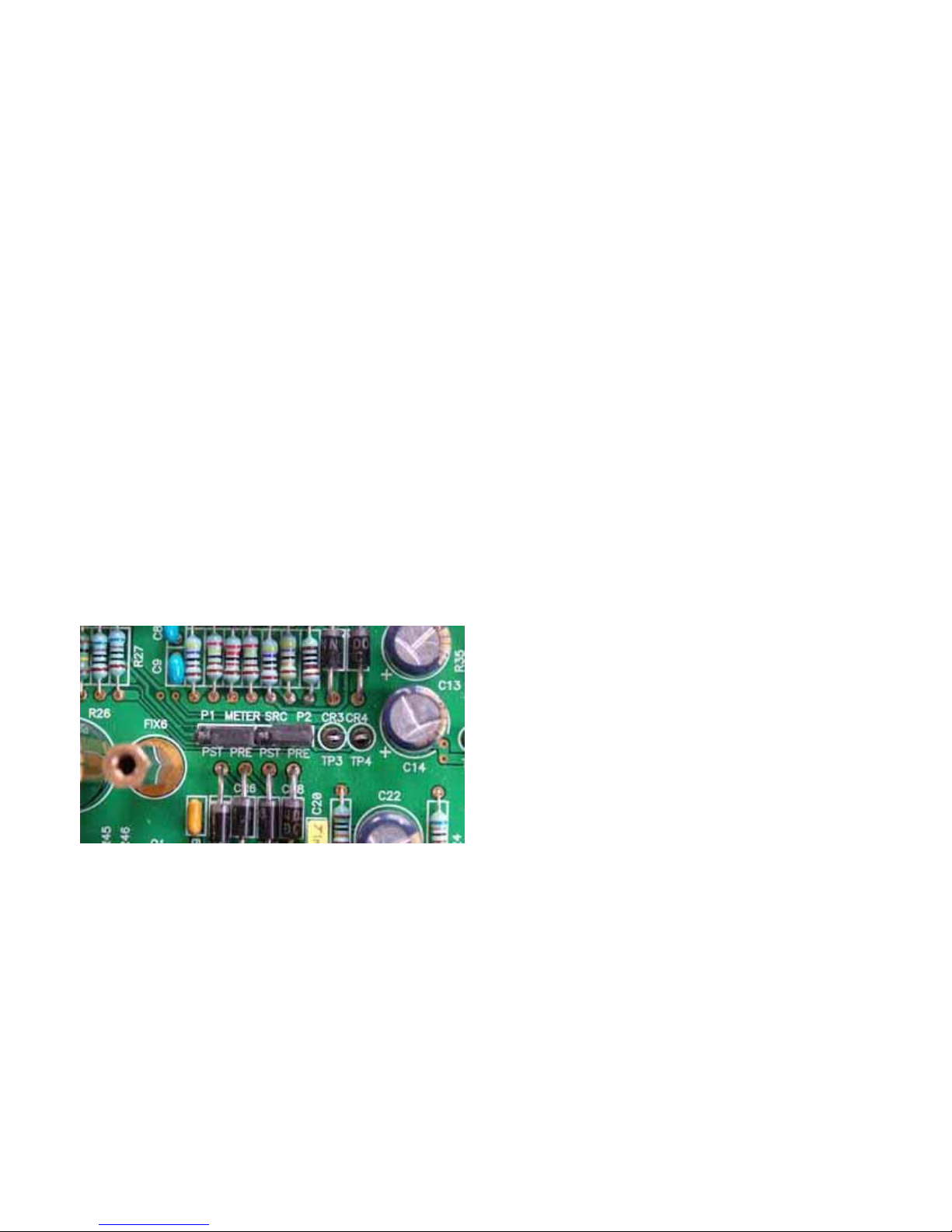
SELECTING MODE OF OPERATION FOR THE METER:
On modules that include output faders, the meter source is normally pre-fader. This is the case because the
fader is an attenuator. The signal level before the fader might be clipping, but with the fader set at say, -10dB,
the output level indicated by a post fader meter would be well below the clipping level.
Therefore the metering source is normally set before the output stage because we want to know the actual
level within the unit, so that hot signals do not clip. The level shown is relative to the ideal final output.
Provision is made for metering after the fader (post) for kit built units. However, the user will have to change a
resistor on the input to rectifier to compensate for additional 5.1dB gain.
 Loading...