


查询U1ZB10供应商
U1ZB6.8~U1ZB390
TOSHIBA ZENER DIODE SILICON DIFFUSED TYPE
U1ZB6.8~U1ZB390
CONSTANT VOLTAGE REGULATION
TRANSIENT SUPPRESSORS
l Average Power Dissipation : P = 1.0 W
l Zener Voltage : V
l Surface Mounting Plastic Mold Package
MAXIMUM RATINGS
CHARACTERISTIC SYMBOL RATING UNIT
Power Dissipation P 1.0 W
Junction Temperature T
Storage Temperature Range T
= 6.8~390 V
Z
(Ta = 25°C)
stg
j
−40~150 °C
−40~150 °C
STANDARD SOLDERING PAD MARK
Unit: mm
JEDEC ―
JEITA ―
TOSHIBA 3−4D1A
Weight: 0.06g
1
2001-07-11
U1ZB6.8~U1ZB390
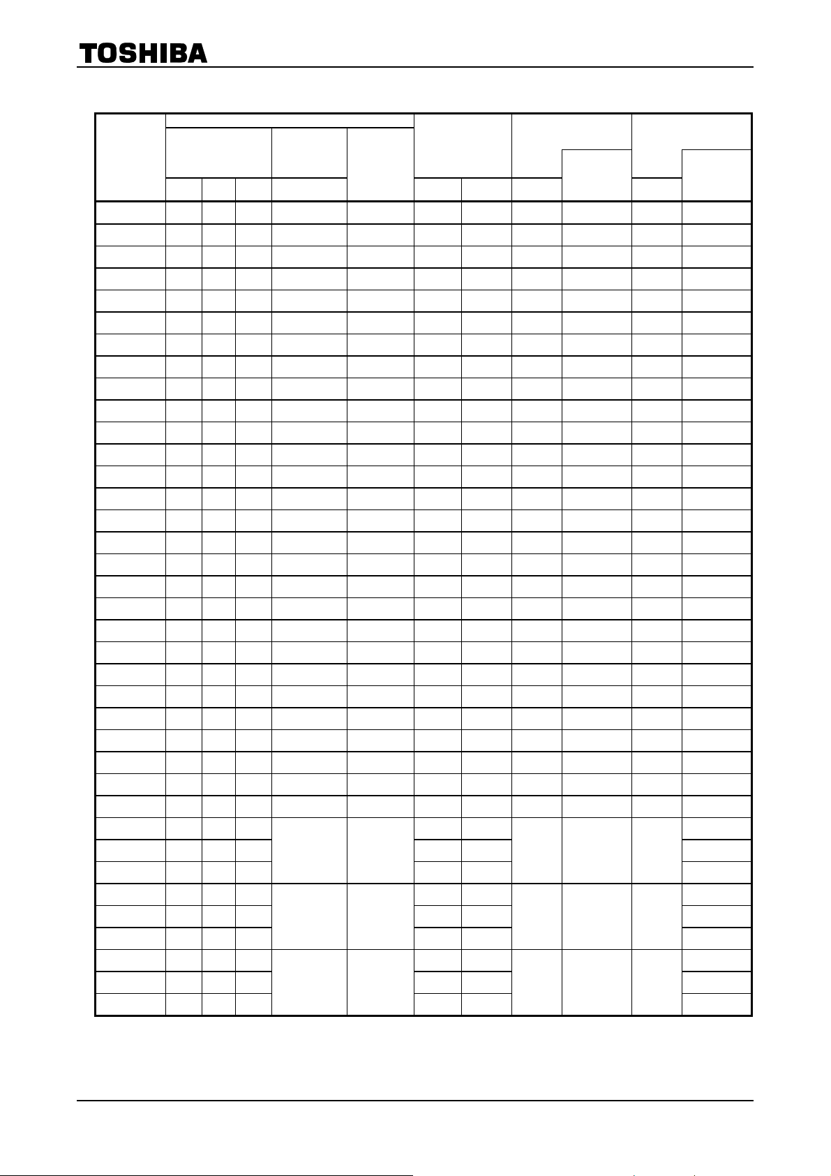
ELECTRICAL CHARACTERISTICS
ZENER CHARACTERISTICS
ZENER
TYPE
U1ZB6.8 6.2 6.8 7.4 60 10 3 4 1.2 0.2 10 3
U1ZB7.5 6.8 7.5 8.3 30 10 4 5 1.2 0.2 10 4.5
U1ZB8.2 7.4 8.2 9.1 30 10 4 6 1.2 0.2 10 4.9
U1ZB9.1 8.2 9.1 10.1 30 10 5 8 1.2 0.2 10 5.5
U1ZB10 9.0 10 11.0 30 10 6 9 1.2 0.2 10 6
U1ZB11 9.9 11 12.1 30 10 7 11 1.2 0.2 10 7
U1ZB12 10.8 12 13.2 30 10 8 13 1.2 0.2 10 8
U1ZB13 11.7 13 14.3 30 10 9 14 1.2 0.2 10 9
U1ZB15 13.5 15 16.5 30 10 11 17 1.2 0.2 10 10
U1ZB16 14.4 16 17.6 30 10 12 19 1.2 0.2 10 11
U1ZB18 16.2 18 19.8 30 10 14 23 1.2 0.2 10 13
U1ZB20 18.0 20 22.0 30 10 16 26 1.2 0.2 10 14
U1ZB22 19.8 22 24.2 30 10 18 28 1.2 0.2 10 16
U1ZB24 21.6 24 26.4 30 10 20 32 1.2 0.2 10 17
U1ZB27 24.3 27 29.7 30 10 23 36 1.2 0.2 10 19
U1ZB30 27.0 30 33.0 30 10 25 40 1.2 0.2 10 21
U1ZB33 29.7 33 36.3 30 10 26 41 1.2 0.2 10 26.4
U1ZB36 32.4 36 39.6 30 9 28 45 1.2 0.2 10 28.8
U1ZB43 38.7 43 47.3 40 7 33 53 1.2 0.2 10 34.4
U1ZB47 42.3 47 51.7 65 6 38 60 1.2 0.2 10 37.6
U1ZB51 45.9 51 56.1 65 6 43 68 1.2 0.2 10 40.8
U1ZB68 61.2 68 74.8 120 4 57 90 1.2 0.2 10 54.4
U1ZB75 67.5 75 82.5 150 4 66 104 1.2 0.2 10 60
U1ZB82 73.8 82 90.2 170 3 71 113 1.2 0.2 10 65.4
U1ZB100 90 100 110 300 3 87 138 1.2 0.2 10 80
U1ZB110 99 110 121 300 3 96 152 1.2 0.2 10 88
U1ZB150 135 150 165 450 2 136 212 1.2 0.2 10 120
U1ZB180 162 180 198 500 1.5 161 255 1.2 0.2 10 144
U1ZB200 180 200 220 170 269 160
U1ZB200−Y 190 200 210 170 269 160
U1ZB200−Z 200 210 220
U1ZB220 198 220 242 200 309 176
U1ZB220−Y 210 220 230 200 309 176
U1ZB220−Z 220 230 240
U1ZB240 216 240 264 215 325 192
U1ZB240−Y 230 240 250 215 325 216
U1ZB240−Z 240 250 260
VOLTAGE
V
MIN TYP. MAX MAX
(V)
Z
ZENER
IMPEDANCE
rd (Ω)
500 0.5
5000 0.5
5000 0.5
(Ta = 25°C)
MEASUREMENT
CURRENT
I
(mA)
Z
TEMPERATURE
COEFFICIENT
OF ZENER
VOLTAGE
αT (mV / °C)
TYP. MAX MAX
178 286
207 320
225 338
VF (V) IR (µA)
1.2 0.2 10
1.2 0.2 10
1.2 0.2 10
FORWARD
VOLTAGE
MEASURE−
MENT
CURRENT
I
(A)
F
REVERSE
CURRENT
MAX
MEASURE−
MENT
VOLTAGE
VR (V)
168
184
225
2
2001-07-11

U1ZB6.8~U1ZB390
ZENER CHARACTERISTICS
ZENER
TYPE
U1ZB270 243 270 297 243 385 216
U1ZB270−X 250 260 270 221 350 234
U1ZB270−Y 260 270 280 228 362 243
U1ZB270−Z 270 280 290
U1ZB300 270 300 330 270 428 240
U1ZB300−X 280 290 300 244 388 261
U1ZB300−Y 290 300 310 253 402 270
U1ZB300−Z 300 310 320
U1ZB330 297 330 363 296 470 264
U1ZB330−X 310 320 330 270 428 288
U1ZB330−Y 320 330 340 278 441 297
U1ZB330−Z 330 340 350
U1ZB390 351 390 429 10000 0.5 350 555 1.2 0.2 10 312
VOLTAGE
V
MIN TYP. MAX MAX.
(V)
Z
ZENER
IMPEDANCE
rd (Ω)
5000 0.5
5000 0.5
5000 0.5
MEASUREMENT
CURRENT
I
(mA)
Z
TEMPERATURE
COEFFICIENT
OF ZENER
VOLTAGE
αT (mV / °C)
TYP. MAX MAX
236 374
261 415
287 455
V
FORWARD
VOLTAGE
(V) IR (µA)
F
1.2 0.2 10
1.2 0.2 10
1.2 0.2 10
MEASURE−
MENT
CURRENT
I
(A)
F
REVERSE
CURRENT
MAX
MEASURE−
MENT
VOLTAGE
V
R
252
279
306
(V)
3
2001-07-11

U1ZB6.8~U1ZB390
4
2001-07-11

U1ZB6.8~U1ZB390
A
RESTRICTIONS ON PRODUCT USE
· TOSHIBA is continually working to improve the quality and reliability of its products. Nevertheless, semiconductor
devices in general can malfunction or fail due to their inherent electrical sensitivity and vulnerability to physical
stress. It is the responsibility of the buyer, when utilizing TOSHIBA products, to comply with the standards of
safety in making a safe design for the entire system, and to avoid situations in which a malfunction or failure of
such TOSHIBA products could cause loss of human life, bodily injury or damage to property.
In developing your designs, please ensure that TOSHIBA products are used within specified operating ranges as
set forth in the most recent TOSHIBA products specifications. Also, please keep in mind the precautions and
conditions set forth in the “Handling Guide for Semiconductor Devices,” or “TOSHIBA Semiconductor Reliability
Handbook” etc..
· The TOSHIBA products listed in this document are intended for usage in general electronics applications
(computer, personal equipment, office equipment, measuring equipment, industrial robotics, domestic appliances,
etc.). These TOSHIBA products are neither intended nor warranted for usage in equipment that requires
extraordinarily high quality and/or reliability or a malfunction or failure of which may cause loss of human life or
bodily injury (“Unintended Usage”). Unintended Usage include atomic energy control instruments, airplane or
spaceship instruments, transportation instruments, traffic signal instruments, combustion control instruments,
medical instruments, all types of safety devices, etc.. Unintended Usage of TOSHIBA products listed in this
document shall be made at the customer’s own risk.
· The information contained herein is presented only as a guide for the applications of our products. No
responsibility is assumed by TOSHIBA CORPORATION for any infringements of intellectual property or other
rights of the third parties which may result from its use. No license is granted by implication or otherwise under
any intellectual property or other rights of TOSHIBA CORPORATION or others.
· The information contained herein is subject to change without notice.
000707EA
5
2001-07-11
 Loading...