

J
C
J
查询TPCP8H01供应商
TOSHIBA Multi-Chip Transistor
Silicon NPN Epitaxial Type, Field Effect Transistor Silicon N Channel MOS Type
TPCP8H01
HIGH-SPEED SWITCHING APPLICATIONS
LORD SWITCHING APPLICATIONS
STROBE FLASH APPLICATIONS
・Multi-chip discrete device; built-in NPN transistor for main switch and
N-ch MOS FET for drive
・High DC current gain: h
・Low collector-emitter saturation voltage: V
= 250 to 400 (IC = 0.5 A) (NPN transistor)
FE
CE (sat)
= 0.13 V (max)
(NPN transistor)
・High-speed switching: t
= 25 ns (typ.) (NPN transistor)
f
Absolute Maximum Ratings
(Ta = 25°C)
Transistor
Characteristics Symbol Rating Unit
Collector-base voltage V
Collector-emitter voltage
Emitter-base voltage V
Collector current
Base current IB
Collector power dissipation (NPN) PC (Note 2)
Junction temperature Tj 150 °C
DC (Note 1)
Pulse (Note 1)
CBO
V
CEX
V
CEO
EBO
I
5.0
C
I
7.0
CP
100
80
50
6
0.5
1.0
V
V
V
A
A
W
MOS FET
EDE
EITA -
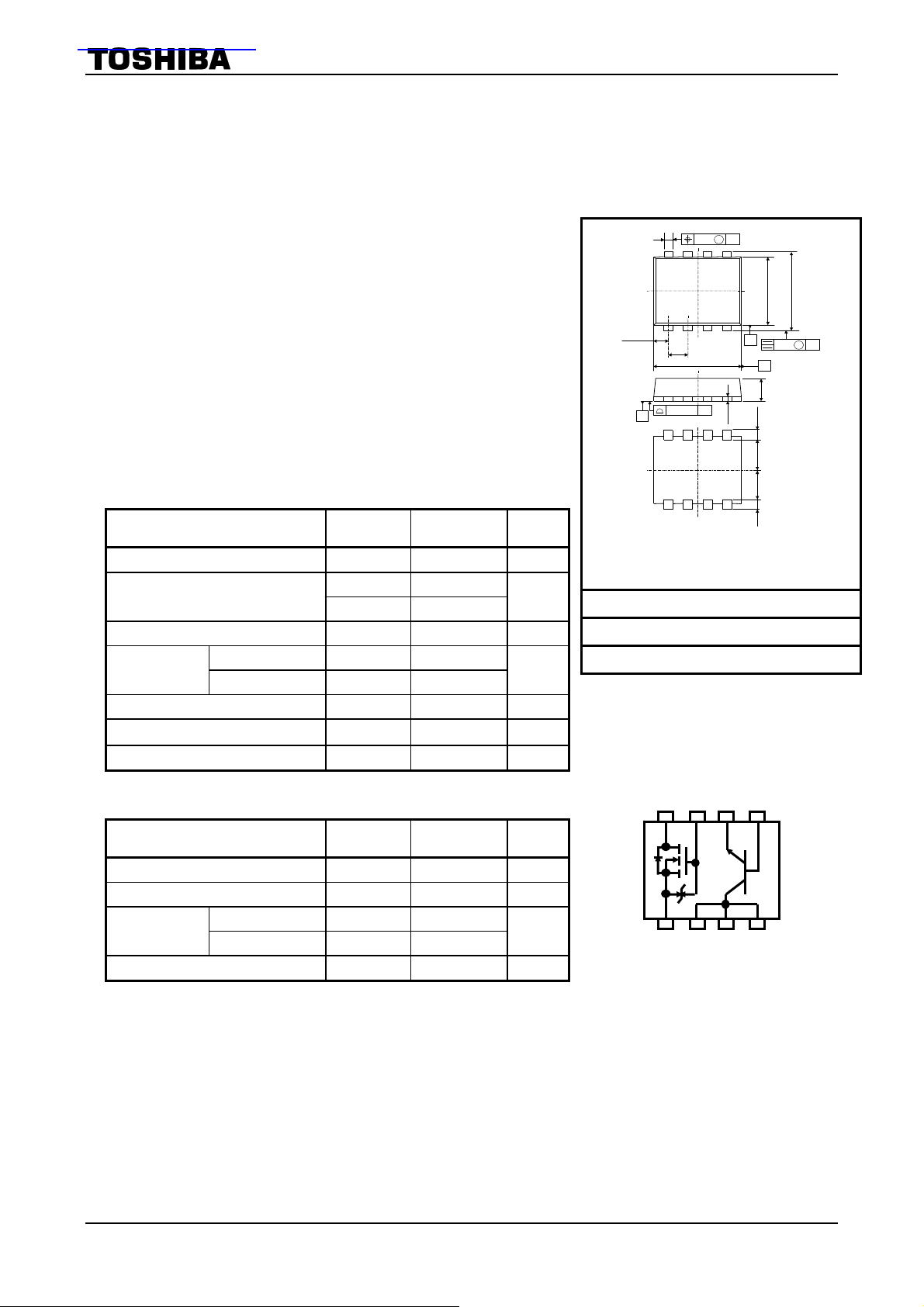
TOSHIBA 2-3V1E
Weight : 0.017g (Typ.)
0.33±0.05
8
0.475
0.025
S
1. SOURCE
2. COLLECTOR
3. COLLECTOR
4. COLLECTOR
0.65
0.05
2.9±0.1
S
0.17±0.02
M
-
Circuit Configuration
TPCP8H01
A
5
2.4±0.1
2.8±0.1
41
B
A
0.8±0.05
0.28
1.12
1.12
0.28
5. BASE
6. EMITTER
7. GATE
8. DRAIN
0.05
+0.1
-0.11
+0.13
-0.12
+0.13
-0.12
+0.1
-0.11
B
M
Characteristics Symbol Rating Unit
Drain-Source Voltage V
Gate-Source Voltage V
Drain Current
Channel Temperature Tch 150 °C
DC
Pulse
DSS
GSS
I
100
D
I
200
DP
20
±10
V
V
mA
1 2 3 4
Note 1: Ensure that the junction (channel) temperature does not exceed 150℃.
Note 2: Device mounted on a glass-epoxy board (FR-4, 25.4×25.4×1.6 mm, Cu area: 645 mm2)
Note 3: Using continuously under heavy loads (e.g. the application of high temperature/current/voltage and the
significant change in temperature, etc.) may cause this product to decrease in the reliability significantly
even if the operating conditions (i.e. operating temperature/current/voltage, etc.) are within the absolute
maximum ratings.
Please design the appropriate reliability upon reviewing the Toshiba Semiconductor Reliability Handbook
(“Handling Precautions”/Derating Concept and Methods) and individual reliability data (i.e. reliability test
report and estimated failure rate, etc).
This transistor is an electrostatic-sensitive device. Please handle with caution.
1
2006-11-13
Common Absolute Maximum Rating (Ta = 25°C)
Characteristics Symbol Rating Unit
TPCP8H01
Storage temperature range T
−55 to 150 °C
stg
Marking (Note 4)
8H01
*
Note 4: The mark “z” on the lower left of the marking indicates Pin 1.
* W
eekly code (three digits)
Type
Lot No.
(Weekly code)
Week of manufacture
(01 for the first week of the year, continuing up to 52 or 53)
Year of manufacture
(Last digit of the of the calendar year)
Electrical Characteristics
(Ta = 25°C)
Transistor
Characteristics Symbol Test Condition Min Typ. Max Unit
V
Collector cut-off current I
Emitter cut-off current I
Collector-emitter breakdown voltage V
DC current gain
Collector-emitter saturation voltage V
Base-emitter saturation voltage V
Collector output capacitance Cob VCB = 10 V, IE = 0, f = 1 MHz
Rise time tr
Switching time
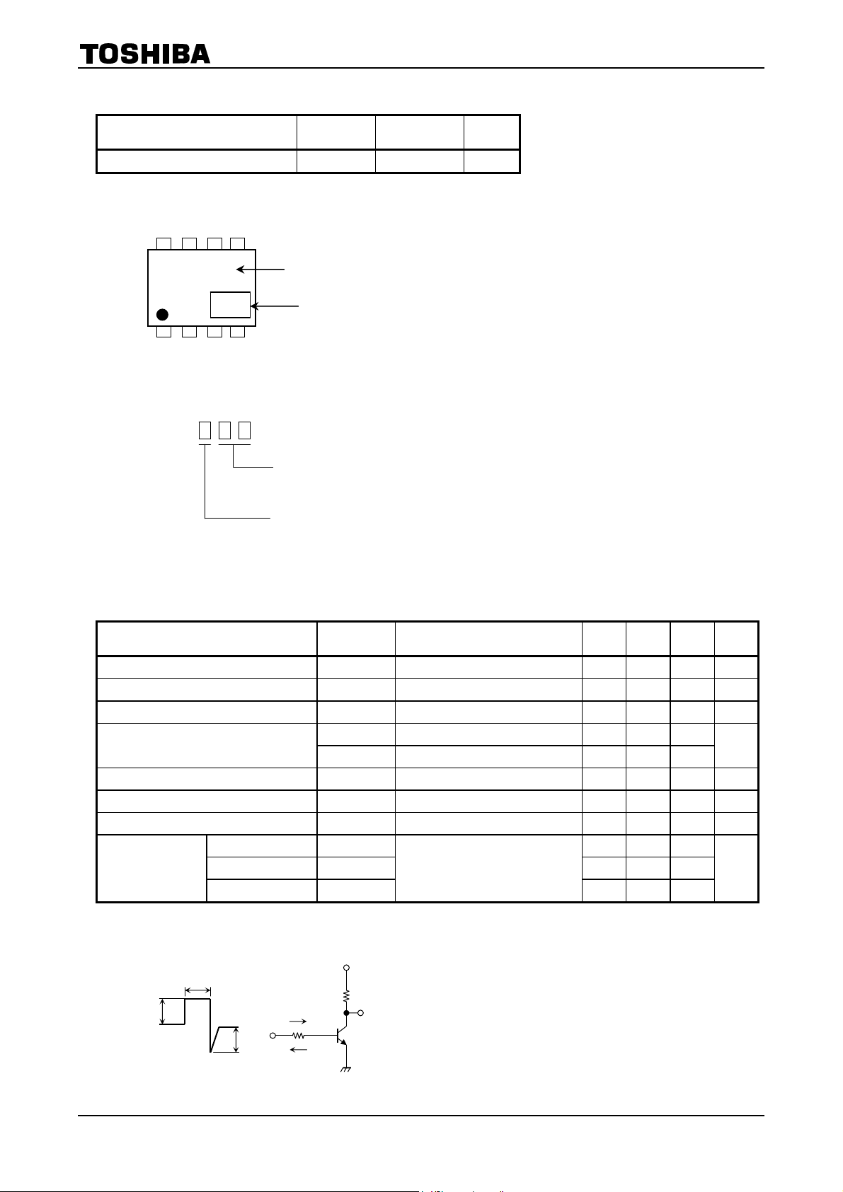
Figure 1 Switching Time Test Circuit & Timing Chart
Storage time t
Fall time t
20 μs
I
B1
Duty cycle < 1%
Input
I
B2
I
B1
I
B2
CBO
EBO
(BR) CEO
hFE (1)
(2)
h
FE
CE (sat)
BE (sat)
stg
f
V
CC
L
R
Output
= 100 V, IE = 0 ⎯ ⎯ 100
CB
V
= 6 V, IC = 0 ⎯ ⎯ 100
EB
IC = 10 mA, IB = 0 50 ⎯ ⎯
VCE = 2 V, IC = 0.5 A 250 ⎯ 400
VCE = 2 V, IC = 1.6 A 100 ⎯ ⎯
I
= 1.6 A, IB = 53 mA ⎯ 80 130
C
I
= 1.6 A, IB = 53 mA ⎯ 0.8 1.1
C
See Figure 1 circuit diagram.
≒ 24 V, RL = 15 Ω
V
CC
= −IB2 = 53 mA
I
B1
⎯ 22 ⎯
⎯ 65 ⎯
⎯ 500 ⎯
⎯ 25 ⎯
nA
nA
V
mV
V
pF
ns
2
2006-11-13
MOS FET
VoutRLVDD
V
Characteristics Symbol Test Condition Min Typ. Max Unit
Gate leakage current I
Drain-Source breakdown voltage V
Drain cut-off current I
Gate threshold voltage V th
Forward transfer admittance |Yfs|
Drain-Source ON resistance R
Input capacitance C
Reverse transfer capacitance C
Output capacitance C
Turn-on time ton
Switching time
Turn-off time t
GSS
(BR)DSS
DSS
DS(ON)
iss
rss
oss
off
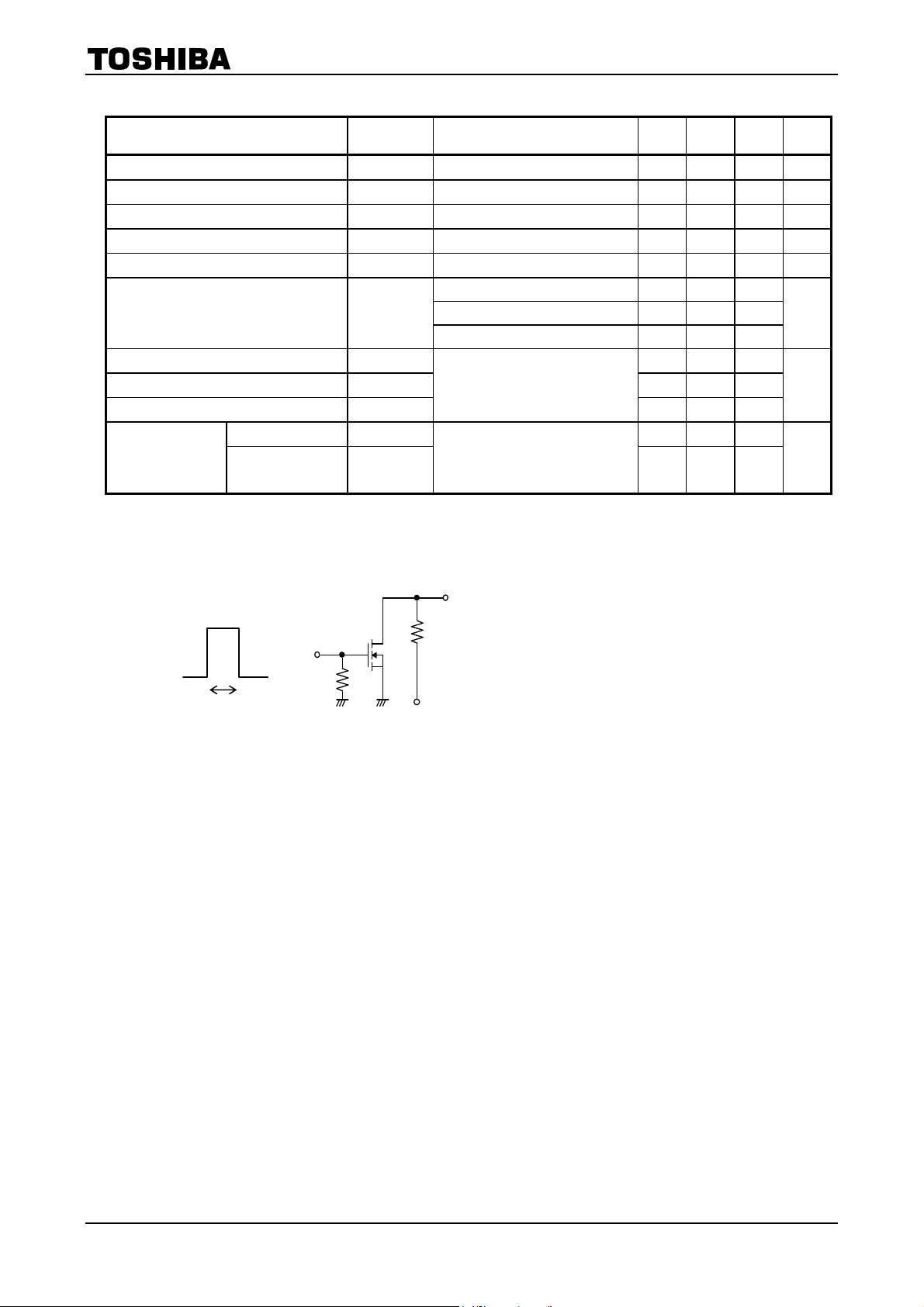
Figure 2 Switching Time Test Circuit &
Timing Chart
2.5V
in
0
10us
Rg
Precautions
V
= ±10 V, VDS = 0 ⎯ ⎯ ±1
GS
= 0.1 mA, VGS = 0 20 ⎯ ⎯
I
D
V
= 20 V, VGS = 0 ⎯ ⎯ 1
DS
= 3 V, ID = 0.1 mA 0.6 ⎯ 1.1
V
DS
V
= 3 V, ID = 10 mA 40 ⎯ ⎯
DS
ID = 10 mA , VGS = 4.0 V ⎯ 1.5 3
ID = 10 mA , VGS = 2.5 V ⎯ 2.2 4
ID = 1 mA , VGS = 1.5 V ⎯ 5.2 15
⎯ 9.3 ⎯
= 3 V, VGS = 0, f= 1 MHz
V
DS
See Figure 2 circuit diagram.
V
≒ 3 V, RL = 300 Ω
DD
= 0 to 2.5 V
V
GS
⎯ 4.5 ⎯
⎯ 9.8 ⎯
⎯ 70 ⎯
⎯ 125 ⎯
Gate Pulse Width 10μs, tr,tf<5ns
(Zout=50Ω),Common Source,Ta=25°C
Duty Cycle<1%
TPCP8H01
μA
V
μA
V
mS
Ω
pF
ns
Vth can be expressed as the voltage between gate and source when the low operating current value is ID=100 μA for
this product. For normal switching operation, V
lower voltage than V
th.
(The relationship can be established as follows: V
Please take this into consideration when using the device. The V
requires a higher voltage than Vth and V
GS (on)
GS (off)
< Vth < V
GS
)
GS (on)
recommended voltage for turning on this
GS (off)
requires a
product is 2.5 V or higher.
3
2006-11-13
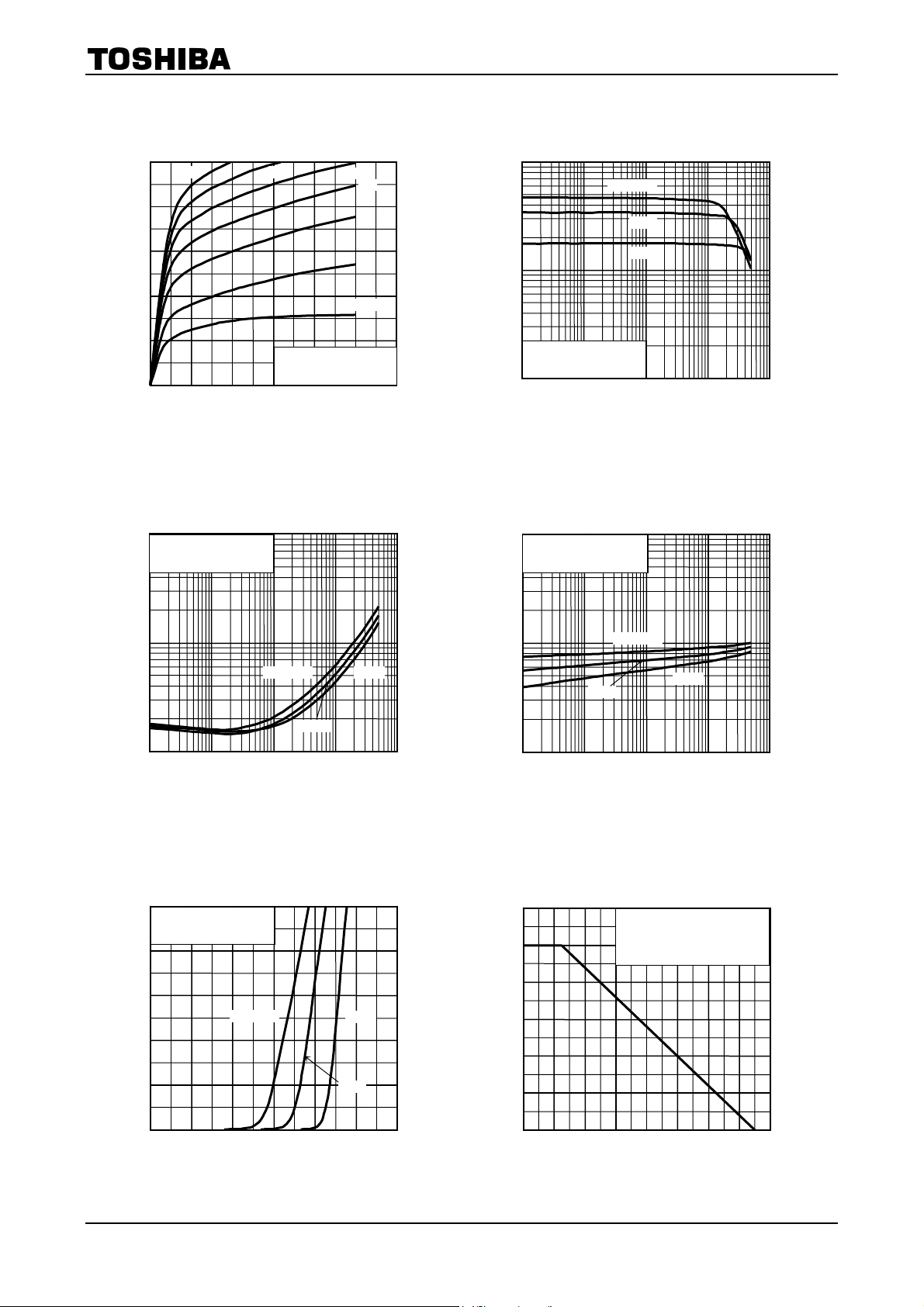
NPN
TPCP8H01
5
60
4
(A)
C
3
2
Collector current I
1
0 0 0.4 0.8 1.6 2.4
Collector−emitter voltage VCE (V)
I
– VCE
C
50
Common emitter
Ta = 25°C
Single nonrepetitive pulse
1.2 2.0
40
30
20
10
IB = 5 mA
1000
FE
100
DC current gain h
Common emitter
VCE = 2 V
Single nonrepetitive pulse
10
0.001
h
– IC
FE
Ta = 100°C
25°C
−55°C
0.01 0.1 1 10
Collector current IC (A)
1
Common emitter
β = 30
Single nonrepetitive pulse
V
CE (sat)
– IC
10
Common emitter
β = 30
Single nonrepetitive pulse
V
BE (sat)
– I
C
(V)
0.1
CE (sat)
V
Ta = 100°C −55°C
Collector−emitter saturation voltage
0.01
0.001
0.01 0.1 1 10
Collector current IC (A)
25°C
(V)
Base−emitter saturation voltage
BE (sat)
V
0.01
1
0.001
Ta = −55°C
100°C
25°C
0.01 0.1 1 10
Collector current IC (A)
5
Common emitter
VCE = 2 V
Single nonrepetitive pulse
4
(A)
C
3
2
Collector current I
1
I
– VBE
C
Ta = 100°C
−55°C
25°C
0 0 0.2 0.8 1.2
0.4 0.6
Base−emitter voltage VBE (V)
1.0
P
– Ta
c
1.2
1.0
(W)
C
0.8
0.6
0.4
0.2
Collector power dissipation P
0
0 20 60 100 160
40 80 140 120
Ambient temperature Ta (°C)
DC operation
Ta = 25 °C
Mounted on an FR4 board glass
epoxy, 1.6 mm thick, Cu area: 645
mm2)
4
2006-11-13

TPCP8H01
1000
(°C/W)
th (j-c)
r
100
10
Transient thermal resistance
1
0.001
Curves should be applied in thermal limited area.
Single nonrepetitive pulse Ta = 25°C
Mounted on FR4 board (glass epoxy, 1.6 mm thick, Cu area: 645 mm2)
Pulse width tw (s)
10 ms*
100 μs* 1 ms*
10 μs*
10
IC max (Pulsed) *
Safe operating area
100 ms*
(A)
C
Collector current I
10 s*
1
DC operation
(Ta = 25°C)
IC max (Continuous)
*: Single nonrepetitive pulse
Ta = 25°C
Note that the curves for 100 ms,
0.1
10 s and DC operation will be
different when the devices aren’t
mounted on an FR4 board
(glass epoxy, 1.6 mm thick, Cu
area: 645 mm2).
These characteristic curves
must be derated linearly with
increase in temperature.
0.01
0.1 1 10 100
Collector−emitter voltage VCE (V)
max
CEO
V
– tw
r
th (j-c)
1 10
1000 0.01 0.1 100
5
2006-11-13

Nch-MOS
TPCP8H01
Drain−source ON resistance
250
3
4
10
2.5
2.3
200
(mA)
D
150
100
Drain current I
50
0
0 0.5
2.1
Drain−source voltage VDS (V)
R
8
Common source
7
6
5
DS (ON)
VGS = 1.5 V, ID = 1 mA
(Ω)
4
DS (ON)
3
R
2
1
0
0 −25
Ambient temperature Ta (°C)
10000
t
off
1000
tf
100
ton
Switching time t (ns)
tr
10
0.1 100 10
1
Drain current ID (mA)
I
– VDS
D
Common source
Ta = 25°C
VGS = 1.3 V
1.0 1.5
– Ta
2.5 V, 10 mA
4.0 V, 10 mA
75 125
100 50 25
t − I
D
Common source
VDD = 3 V
VGS = 0~2.5V
Ta = 25°C
1.9
1.5
1.7
2.0
150
12
Common source
Ta = 25°C
10
8
(Ω)
6
DS (ON)
R
4
2
Drain−source ON resistance
0
1
1000
Common source
VDS = 3 V
Ta = 25°C
100
⎪ (S)
fs
⎪Y
10
Forward transfer admittance
1
1
100
10
Capacitance C (pF)
1
0.1
DS (ON)
− ID
R
VGS = 1.5 V
10 100
Drain current ID (mA)
⎪Y
⎪ − I
fs
D
10 100
Drain current ID (mA)
Capacitance − V
1
Drain−source voltage V
2.5
4
DS
Common source
VGS = 0 V
f = 1 MHz
Ta = 25°C
C
iss
C
oss
C
rss
10
(V)
DS
1000
1000
100
6
2006-11-13

1000
Common source
VDS = 3 V
100
(mA)
D
10
Drain current I
0.1
0.01
Ta = 100°C
1
0
Gate−source voltage V
2.0
Common source
ID = 0.1 mA
V
= 3 V
(V)
th
DS
1.6
1.2
0.8
0.4
Gate threshold voltage V
0
−25 25
0 50 125 100
Ambient temperature Ta (°C)
I
− VGS
D
−25
25
1 2
(V)
GS
V
− Ta
th
75
150
TPCP8H01
8
Common source
ID = 10 mA
6
(Ω)
4
DS (ON)
R
2
Drain−source ON resistance
3
0
250
Common source
VGS = 0 V
DR
200
150
Ta = 25°C
(mA)
100
50
Drain reverse current I
0
−0.20
R
25
20
− VGS
DS (ON)
Ta =100°C
46 8
Gate−source voltage V
I
− V
DR
DS
−0.4 −1.0 −1.2 −0.8
−0.6
Drain−source voltage V
−25
GS
DS
10
(V)
−1.4
(V)
7
2006-11-13

TPCP8H01
RESTRICTIONS ON PRODUCT USE
• The information contained herein is subject to change without notice.
• TOSHIBA is continually working to improve the quality and reliability of its products. Nevertheless, semiconductor
devices in general can malfunction or fail due to their inherent electrical sensitivity and vulnerability to physical
stress. It is the responsibility of the buyer, when utilizing TOSHIBA products, to comply with the standards of
safety in making a safe design for the entire system, and to avoid situations in which a malfunction or failure of
such TOSHIBA products could cause loss of human life, bodily injury or damage to property.
In developing your designs, please ensure that TOSHIBA products are used within specified operating ranges as
set forth in the most recent TOSHIBA products specifications. Also, please keep in mind the precautions and
conditions set forth in the “Handling Guide for Semiconductor Devices,” or “TOSHIBA Semiconductor Reliability
Handbook” etc.
• The TOSHIBA products listed in this document are intended for usage in general electronics applications
(computer, personal equipment, office equipment, measuring equipment, industrial robotics, domestic appliances,
etc.).These TOSHIBA products are neither intended nor warranted for usage in equipment that requires
extraordinarily high quality and/or reliability or a malfunction or failure of which may cause loss of human life or
bodily injury (“Unintended Usage”). Unintended Usage include atomic energy control instruments, airplane or
spaceship instruments, transportation instruments, traffic signal instruments, combustion control instruments,
medical instruments, all types of safety devices, etc.. Unintended Usage of TOSHIBA products listed in his
document shall be made at the customer’s own risk.
• The products described in this document shall not be used or embedded to any downstream products of which
manufacture, use and/or sale are prohibited under any applicable laws and regulations.
• The information contained herein is presented only as a guide for the applications of our products. No
responsibility is assumed by TOSHIBA for any infringements of patents or other rights of the third parties which
may result from its use. No license is granted by implication or otherwise under any patents or other rights of
TOSHIBA or the third parties.
20070701-EN
• Please contact your sales representative for product-by-product details in this document regarding RoHS
compatibility. Please use these products in this document in compliance with all applicable laws and regulations
that regulate the inclusion or use of controlled substances. Toshiba assumes no liability for damage or losses
occurring as a result of noncompliance with applicable laws and regulations.
8
2006-11-13
 Loading...