

TOSHIBA TPCC8131 Datasheet

MOSFETs Silicon P-Channel MOS (U-MOS)
TSON Advance
TPCC8131
TPCC8131
TPCC8131
TPCC8131
1.
Applications
1.
Applications
1.
1. Applications
Applications
• Lithium-Ion Secondary Batteries
• Power Management Switches
2.
Features
2.
Features
2.
2. Features
Features
(1) Small, thin package
(2) Low drain-source on-resistance: R
(3) Low leakage current: I
(4) Enhancement mode: Vth = -0.8 to -2.0 V (VDS = -10 V, ID = -0.2 mA)
3.
Packaging and Internal Circuit
3.
Packaging and Internal Circuit
3.
3. Packaging and Internal Circuit
Packaging and Internal Circuit
= -10 µA (max) (VDS = -30 V)
DSS
= 13.5 mΩ (typ.) (VGS = -10 V)
DS(ON)
TPCC8131
1, 2, 3: Source
4: Gate
5, 6, 7, 8: Drain
4.
Absolute Maximum Ratings (Note) (T
4.
Absolute Maximum Ratings (Note) (T
4.
4. Absolute Maximum Ratings (Note) (T
Absolute Maximum Ratings (Note) (T
Characteristics
Drain-source voltage
Gate-source voltage
Drain current (DC)
Drain current (pulsed)
Power dissipation
Power dissipation
Power dissipation
Single-pulse avalanche energy
Avalanche current
Channel temperature
Storage temperature
Note: Using continuously under heavy loads (e.g. the application of high temperature/current/voltage and the
significant change in temperature, etc.) may cause this product to decrease in the reliability significantly even
if the operating conditions (i.e. operating temperature/current/voltage, etc.) are within the absolute maximum
ratings.
Please design the appropriate reliability upon reviewing the Toshiba Semiconductor Reliability Handbook
("Handling Precautions"/"Derating Concept and Methods") and individual reliability data (i.e. reliability test
report and estimated failure rate, etc).
(Tc = 25)
(t = 10 s)
(t = 10 s)
= 25
= 25
= 25
= 25
a
a
a
a
unless otherwise specified)
unless otherwise specified)
unless otherwise specified)
unless otherwise specified)
(Note 1)
(Note 1)
(Note 2)
(Note 3)
(Note 4)
Symbol
V
DSS
V
GSS
I
D
I
DP
P
D
PD
P
D
E
AS
I
AR
T
ch
T
stg
Rating
-30
-25/+20
-10
-30
20
1.9
0.7
65
-10
150
-55 to 150
Start of commercial production
1
2014-02-17
Unit
V
A
W
W
W
mJ
A
2010-12
Rev.3.0

5.
Thermal Characteristics
5.
Thermal Characteristics
5.
5. Thermal Characteristics
Thermal Characteristics
TPCC8131
Characteristics
Channel-to-case thermal resistance
Channel-to-ambient thermal resistance
Channel-to-ambient thermal resistance
Note 1: Ensure that the channel temperature does not exceed 150.
Note 2: Device mounted on a glass-epoxy board (a), Figure 5.1
Note 3: Device mounted on a glass-epoxy board (b), Figure 5.2
Note 4: VDD = -24 V, Tch = 25 (initial), L = 0.5 mH, RG = 25 Ω, IAR = -10 A
Fig.
5.1
Fig.
Fig.
Fig. 5.1
Note: This transistor is sensitive to electrostatic discharge and should be handled with care.
Device Mounted on a Glass-Epoxy
5.1
Device Mounted on a Glass-Epoxy
5.1 Device Mounted on a Glass-Epoxy
Device Mounted on a Glass-Epoxy
Board (a)
Board (a)
Board (a)
Board (a)
(Tc = 25)
(t = 10 s)
(t = 10 s)
(Note 2)
(Note 3)
Fig.
5.2
Fig.
Fig.
Fig. 5.2
Device Mounted on a Glass-Epoxy
5.2
Device Mounted on a Glass-Epoxy
5.2 Device Mounted on a Glass-Epoxy
Device Mounted on a Glass-Epoxy
Symbol
R
th(ch-c)
R
th(ch-a)
R
th(ch-a)
Board (b)
Board (b)
Board (b)
Board (b)
Max
6.25
65.7
178
Unit
/W
/W
2
2014-02-17
Rev.3.0
6.
Electrical Characteristics
6.
Electrical Characteristics
6.
6. Electrical Characteristics
Electrical Characteristics
6.1.
Static Characteristics (T
6.1.
Static Characteristics (T
6.1.
6.1. Static Characteristics (T
Static Characteristics (T
= 25
= 25
= 25
= 25
a
a
a
a
unless otherwise specified)
unless otherwise specified)
unless otherwise specified)
unless otherwise specified)
TPCC8131
Characteristics
Gate leakage current
Drain cut-off current
Drain-source breakdown voltage
Drain-source breakdown voltage
Gate threshold voltage
Drain-source on-resistance
Note 5: If a forward bias is applied between gate and source, this device enters V
source breakdown voltage is lowered in this mode.
6.2.
Dynamic Characteristics (T
6.2.
Dynamic Characteristics (T
6.2.
6.2. Dynamic Characteristics (T
Dynamic Characteristics (T
Characteristics
Input capacitance
Reverse transfer capacitance
Output capacitance
Switching time (rise time)
Switching time (turn-on time)
Switching time (fall time)
Switching time (turn-off time)
(Note 5)
Symbol
I
GSS
I
DSS
V
(BR)DSS
V
(BR)DSX
V
R
DS(ON)
= 25
= 25
= 25
= 25
a
a
a
a
Symbol
C
iss
C
rss
C
oss
t
r
t
on
t
f
t
off
Test Condition
VGS = ±20 V, VDS = 0 V
VDS = -30 V, VGS = 0 V
ID = -10 mA, VGS = 0 V
ID = -10 mA, VGS = 10 V
VDS = -10 V, ID = -0.2 mA
th
VGS = -4.5 V, ID = -5 A
VGS = -10 V, ID = -5 A
unless otherwise specified)
unless otherwise specified)
unless otherwise specified)
unless otherwise specified)
Test Condition
VDS = -10 V, VGS = 0 V, f = 1 MHz
See Figure 6.2.1.
Min
-30
-21
-0.8
(BR)DSX
Min
Typ.
17.6
13.5
mode. Note that the drain-
Typ.
1700
280
320
5.2
14
52
170
Max
±0.1
-10
-2.0
23
17.6
Max
Unit
µA
V
mΩ
Unit
pF
ns
Fig.
6.2.1
Fig.
6.2.1
Fig.
Fig. 6.2.1
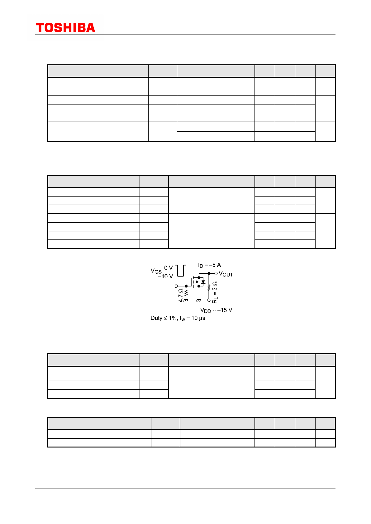
6.2.1 Switching Time Test Circuit
6.3.
Gate Charge Characteristics (T
6.3.
Gate Charge Characteristics (T
6.3.
6.3. Gate Charge Characteristics (T
Gate Charge Characteristics (T
Characteristics
Total gate charge (gate-source plus
gate-drain)
Gate-source charge 1
Gate-drain charge
6.4.
Source-Drain Characteristics (T
6.4.
Source-Drain Characteristics (T
6.4.
6.4. Source-Drain Characteristics (T
Source-Drain Characteristics (T
Characteristics
Reverse drain current (pulsed)
Diode forward voltage
Note 6: Ensure that the channel temperature does not exceed 150.
Symbol
Q
Q
(Note 6)
Switching Time Test Circuit
Switching Time Test Circuit
Switching Time Test Circuit
= 25
unless otherwise specified)
unless otherwise specified)
unless otherwise specified)
unless otherwise specified)
Test Condition
≈ -24 V, V
DD
unless otherwise specified)
unless otherwise specified)
unless otherwise specified)
unless otherwise specified)
IDR = -10 A, VGS = 0 V
Q
g
gs1
gd
= 25
= 25
= 25
a
a
a
a
= 25
= 25
= 25
= 25
a
a
a
a
Symbol
I
DRP
V
DSF
V
3
= -10 V, ID = -10 A
GS
Test Condition
Min
Min
Typ.
40
4.5
11
Typ.
Max
Max
-30
1.2
Unit
nC
Unit
A
V
2014-02-17
Rev.3.0
 Loading...