

MOSFETs Silicon N-Channel MOS (U-MOS-H)
SOP Advance
TPCA8057-H
TPCA8057-H
TPCA8057-H
TPCA8057-H
1.
Applications
1.
Applications
1.
1. Applications
Applications
• High-Efficiency DC-DC Converters
• Notebook PCs
• Mobile Equipment
2.
Features
2.
Features
2.
2. Features
Features
(1) Small footprint due to a small and thin package
(2) High-speed switching
(3) Small gate charge: QSW = 14 nC (typ.)
(4) Low drain-source on-resistance: R
(5) Low leakage current: I
(6) Enhancement mode: Vth = 1.3 to 2.3 V (VDS = 10 V, ID = 0.5 mA)
3.
Packaging and Internal Circuit
3.
Packaging and Internal Circuit
3.
3. Packaging and Internal Circuit
Packaging and Internal Circuit
= 10 µA (max) (VDS = 30 V)
DSS
= 2.6 mΩ (typ.) (VGS = 4.5 V)
DS(ON)
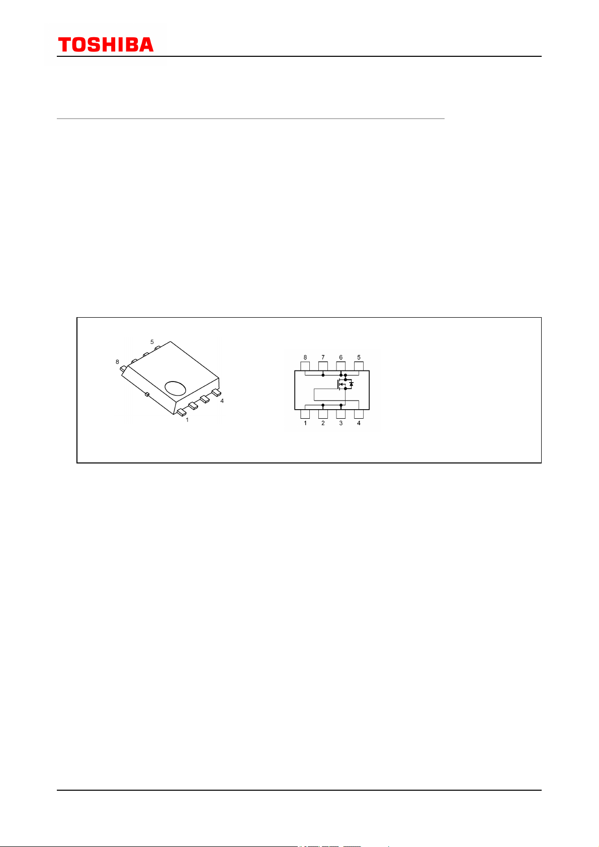
TPCA8057-H
1, 2, 3: Source
4: Gate
5, 6, 7, 8: Drain
Start of commercial production
2010-04
1
2014-03-04
Rev.2.0
4.
Absolute Maximum Ratings (Note) (T
4.
Absolute Maximum Ratings (Note) (T
4.
4. Absolute Maximum Ratings (Note) (T
Absolute Maximum Ratings (Note) (T
= 25
= 25
= 25
= 25
a
a
a
a
TPCA8057-H
unless otherwise specified)
unless otherwise specified)
unless otherwise specified)
unless otherwise specified)
Characteristics
Drain-source voltage
Gate-source voltage
Drain current (DC)
Drain current (pulsed)
Power dissipation
Power dissipation
Power dissipation
Single-pulse avalanche energy
Avalanche current
Channel temperature
Storage temperature
Note: Using continuously under heavy loads (e.g. the application of high temperature/current/voltage and the
significant change in temperature, etc.) may cause this product to decrease in the reliability significantly even
if the operating conditions (i.e. operating temperature/current/voltage, etc.) are within the absolute maximum
ratings.
Please design the appropriate reliability upon reviewing the Toshiba Semiconductor Reliability Handbook
("Handling Precautions"/"Derating Concept and Methods") and individual reliability data (i.e. reliability test
report and estimated failure rate, etc).
5.
Thermal Characteristics
5.
Thermal Characteristics
5.
5. Thermal Characteristics
Thermal Characteristics
Channel-to-case thermal resistance
Channel-to-ambient thermal resistance
Channel-to-ambient thermal resistance
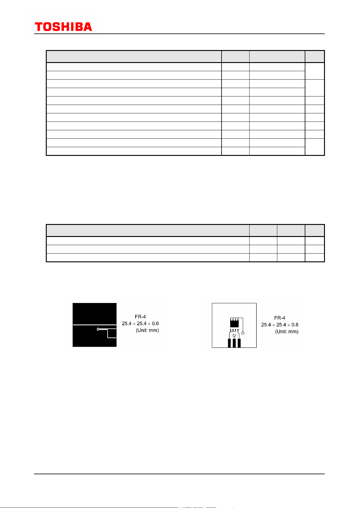
Note 1: Ensure that the channel temperature does not exceed 150 .
Note 2: Device mounted on a glass-epoxy board (a), Figure 5.1
Note 3: Device mounted on a glass-epoxy board (b), Figure 5.2
Note 4: VDD = 24 V, Tch = 25 (initial), L = 0.1 mH, RG = 1 Ω, IAR = 42 A
(Tc = 25 )
(t = 10 s)
(t = 10 s)
Characteristics
(Note 1)
(Note 1)
(Note 2)
(Note 3)
(Note 4)
(Tc = 25 )
(t = 10 s)
(t = 10 s)
Symbol
V
V
I
P
P
P
E
I
T
T
(Note 2)
(Note 3)
DSS
GSS
I
D
DP
D
D
D
AS
AR
ch
stg
-55 to 150
Symbol
R
th(ch-c)
R
th(ch-a)
R
th(ch-a)
Rating
30
±20
42
126
57
2.8
1.6
229
42
150
Max
2.19
44.6
78.1
Unit
V
A
W
W
W
mJ
A
Unit
/W
/W
/W
Fig.
5.1
Fig.
Fig.
Fig. 5.1
Note: This transistor is sensitive to electrostatic discharge and should be handled with care.
Device Mounted on a Glass-Epoxy
5.1
Device Mounted on a Glass-Epoxy
5.1 Device Mounted on a Glass-Epoxy
Device Mounted on a Glass-Epoxy
Board (a)
Board (a)
Board (a)
Board (a)
Fig.
5.2
Fig.
Fig.
Fig. 5.2
Device Mounted on a Glass-Epoxy
5.2
Device Mounted on a Glass-Epoxy
5.2 Device Mounted on a Glass-Epoxy
Device Mounted on a Glass-Epoxy
Board (b)
Board (b)
Board (b)
Board (b)
2
2014-03-04
Rev.2.0
6.
Electrical Characteristics
6.
Electrical Characteristics
6.
6. Electrical Characteristics
Electrical Characteristics
6.1.
Static Characteristics (T
6.1.
Static Characteristics (T
6.1.
6.1. Static Characteristics (T
Static Characteristics (T
= 25
= 25
= 25
= 25
a
a
a
a
unless otherwise specified)
unless otherwise specified)
unless otherwise specified)
unless otherwise specified)
TPCA8057-H
Characteristics
Gate leakage current
Drain cut-off current
Drain-source breakdown voltage
Gate threshold voltage
Drain-source on-resistance
6.2.
Dynamic Characteristics (T
6.2.
Dynamic Characteristics (T
6.2.
6.2. Dynamic Characteristics (T
Dynamic Characteristics (T
Characteristics
Input capacitance
Reverse transfer capacitance
Output capacitance
Gate resistance
Switching time (rise time)
Switching time (turn-on time)
Switching time (fall time)
Switching time (turn-off time)
Symbol
I
GSS
I
DSS
V
(BR)DSS
V
(BR)DSX
V
R
DS(ON)
= 25
= 25
= 25
= 25
a
a
a
a
Symbol
C
iss
C
rss
C
oss
r
g
t
r
t
on
t
f
t
off
Test Condition
VGS = ±20 V, VDS = 0 V
VDS = 30 V, VGS = 0 V
ID = 10 mA, VGS = 0 V
ID = 10 mA, VGS = -20 V
VDS = 10 V, ID = 0.5 mA
th
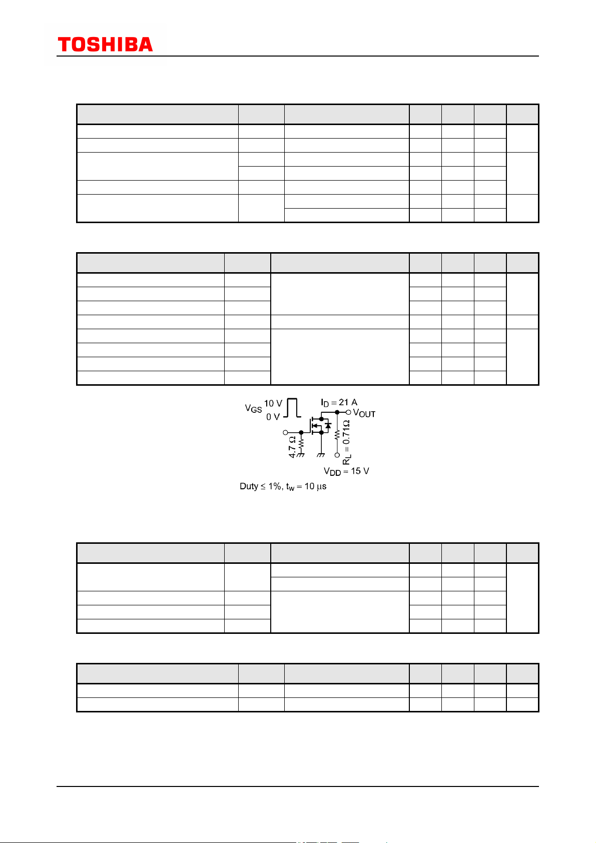
VGS = 4.5 V, ID = 21 A
VGS = 10 V, ID = 21 A
unless otherwise specified)
unless otherwise specified)
unless otherwise specified)
unless otherwise specified)
Test Condition
VDS = 10 V, VGS = 0 V, f = 1 MHz
VDS = 10 V, VGS = 0 V, f = 5 MHz
See Fig. 6.2.1.
Min
30
15
1.3
Min
Typ.
2.6
2.0
Typ.
4300
240
810
1.4
4.3
14
6.3
52
Max
±0.1
10
2.3
3.2
2.6
Max
5200
370
2.1
Unit
µA
V
mΩ
Unit
pF
Ω
ns
Fig.
6.2.1
Fig.
6.2.1
Fig.
Fig. 6.2.1
6.2.1 Switching Time Test Circuit
6.3.
Gate Charge Characteristics (T
6.3.
Gate Charge Characteristics (T
6.3.
6.3. Gate Charge Characteristics (T
Gate Charge Characteristics (T
Characteristics
Total gate charge (gate-source plus
gate-drain)
Gate-source charge 1
Gate-drain charge
Gate switch charge
6.4.
Source-Drain Characteristics (T
6.4.
Source-Drain Characteristics (T
6.4.
6.4. Source-Drain Characteristics (T
Source-Drain Characteristics (T
Characteristics
Reverse drain current (pulsed)
Diode forward voltage
Note 5: Ensure that the channel temperature does not exceed 150 .
Symbol
Q
Q
Q
(Note 5)
Switching Time Test Circuit
Switching Time Test Circuit
Switching Time Test Circuit
= 25
unless otherwise specified)
unless otherwise specified)
unless otherwise specified)
unless otherwise specified)
Test Condition
≈ 24 V, V
DD
≈ 24 V, V
DD
≈ 24 V, V
DD
IDR = 42 A, VGS = 0 V
GS
GS
GS
unless otherwise specified)
unless otherwise specified)
unless otherwise specified)
unless otherwise specified)
Test Condition
Q
g
gs1
gd
SW
Symbol
I
DRP
V
= 25
= 25
= 25
a
a
a
a
V
V
V
= 25
= 25
= 25
= 25
a
a
a
a
DSF
= 10 V, ID = 42 A
= 5 V, ID = 42 A
= 10 V, ID = 42 A
Min
Min
Typ.
61
31
13
7.7
14
Typ.
Max
Max
126
-1.2
Unit
nC
Unit
A
V
3
2014-03-04
Rev.2.0
 Loading...