

TOSHIBA TPCA8030-H Datasheet
TPCA8030-H
S
A
8 5
A
TOSHIBA Field Effect Transistor Silicon N-Channel MOS Type (U-MOS V-H)
TPCA8030-H
High-Efficiency DC-DC Converter Applications
4
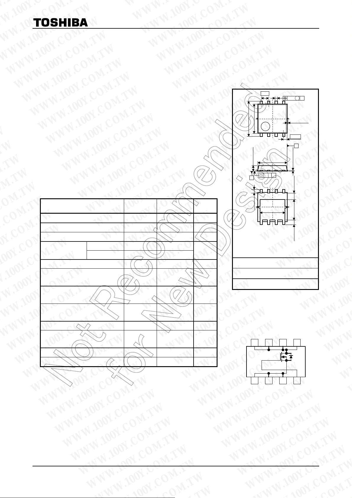
Unit: mm
0.05 M
0.15 ± 0.05
0.595
0.166 ± 0.05
4
0.8 ± 0.1 3.5 ± 0.2 1.1 ± 0.2
Notebook PC Applications
Portable Equipment Applications
• Small footprint due to a small and thin package
• High-speed switching
• Small gate charge: Q
• Low drain-source ON-resistance: R
• High forward transfer admittance: |Y
• Low leakage current: I
• Enhancement mode: V
Absolute Maximum Ratings
Characteristic Symbol Rating Unit
Drain-source voltage
Drain-gate voltage (RGS = 20 kΩ)
Gate-source voltage
Drain current
Drain power dissipation (Tc=25℃) PD 30 W
Drain power dissipation (t = 10 s)
(Note 2a)
Drain power dissipation (t = 10 s)
(Note 2b)
Single-pulse avalanche energy
Avalanche current IAR 24 A
WWW.100Y.COM.TW WWW.100Y.COM.TW WWW.100Y.COM.TW
WWW.100Y.COM.TW WWW.100Y.COM.TW WWW.100Y.COM.TW
WWW.100Y.COM.TW WWW.100Y.COM.TW WWW.100Y.COM.TW
Repetitive avalanche energy
(Tc = 25℃) (Note 4)
Channel temperature
Storage temperature range
= 5.0 nC (typ.)
SW
DS (ON)
= 10 μA (max) (VDS = 30 V)
DSS
= 1.5 to 2.5 V (VDS = 10 V, ID = 1 mA)
th
(Ta = 25°C)
DC (Note 1) ID 24
Pulsed (Note 1) I
(Note 3)
= 7.3 mΩ (typ.)
| = 60 S (typ.)
fs
V
30 V
DSS
V
30 V
DGR
V
±20 V
GSS
72
DP
P
2.8 W
D
P
1.6 W
D
75 mJ
E
AS
E
3.0 mJ
AR
T
150 °C
ch
T
−55 to 150 °C
stg
A
6.0 ± 0.3
0.95 ± 0.05
S
1,2,3:SOURCE 4:GATE
5,6,7,8:DRAIN
JEDEC ⎯
JEITA ⎯
TOSHIBA 2-5Q1A
Weight: 0.069 g (typ.)
Circuit Configuration
0.4 ± 0.1
1.27
5.0 ± 0.2
1
5.0 ± 0.2
0.05
1
0.6 ± 0.1
4.25 ± 0.2
8 5
8 6
7 5
Note: For Notes 1 to 4, refer to the next page.
WWW.100Y.COM.TW WWW.100Y.COM.TW WWW.100Y.COM.TW
WWW.100Y.COM.TW WWW.100Y.COM.TW WWW.100Y.COM.TW
Using continuously under heavy loads (e.g. the application of high
temperature/current/voltage and the significant change in
temperature, etc.) may cause this product to decrease in the
WWW.100Y.COM.TW WWW.100Y.COM.TW WWW.100Y.COM.TW
reliability significantly even if the operating conditions (i.e. operating temperature/current/voltage, etc.) are
within the absolute maximum ratings. Please design the appropriate reliability upon reviewing the Toshiba
WWW.100Y.COM.TW WWW.100Y.COM.TW WWW.100Y.COM.TW
Semiconductor Reliability Handbook (“Handling Precautions”/“Derating Concept and Methods”) and individual
reliability data (i.e. reliability test report and estimated failure rate, etc).
WWW.100Y.COM.TW WWW.100Y.COM.TW WWW.100Y.COM.TW
This transistor is an electrostatic-sensitive device. Handle with care.
1 2 3
4
WWW.100Y.COM.TW WWW.100Y.COM.TW WWW.100Y.COM.TW
WWW.100Y.COM.TW WWW.100Y.COM.TW WWW.100Y.COM.TW
WWW.100Y.COM.TW WWW.100Y.COM.TW WWW.100Y.COM.TW
1
2008-06-20
WWW.100Y.COM.TW WWW.100Y.COM.TW WWW.100Y.COM.TW
Thermal Characteristics
Characteristic Symbol Max Unit
TPCA8030-H
Thermal resistance, channel to case
(Tc = 25℃)
Thermal resistance, channel to ambient
(t = 10 s) (Note 2a)
Thermal resistance, channel to ambient
(t = 10 s) (Note 2b)
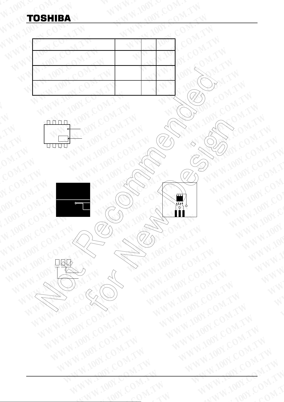
Marking
Note 1: Ensure that the channel temperature does not exceed 150°C.
Note 2: (a) Device mounted on a glass-epoxy board (a) (b) Device mounted on a glass-epoxy board (b)
(Note 5)
8030-H
※
Part number TPCA
Lot No.
R
R
R
4.17 °C/W
th (ch-c)
44.6 °C/W
th (ch-a)
78.1 °C/W
th (ch-a)
Note 3: V
Note 4: Repetitive rating: pulse width limited by maximum channel temperature
Note 5:
DD
* Weekly code: (Three digits)
WWW.100Y.COM.TW WWW.100Y.COM.TW WWW.100Y.COM.TW
WWW.100Y.COM.TW WWW.100Y.COM.TW WWW.100Y.COM.TW
(a)
= 24 V, Tch = 25°C (initial), L = 100 μH, RG = 25 Ω, IAR = 24 A
Week of manufacture
(01 for the first week of the year, continuing up to 52 or 53)
Year of manufacture
(The last digit of the year)
FR-4
25.4 × 25.4 × 0.8
(Unit: mm)
FR-4
25.4 × 25.4 × 0.8
(Unit: mm)
(b)
WWW.100Y.COM.TW WWW.100Y.COM.TW WWW.100Y.COM.TW
WWW.100Y.COM.TW WWW.100Y.COM.TW WWW.100Y.COM.TW
WWW.100Y.COM.TW WWW.100Y.COM.TW WWW.100Y.COM.TW
WWW.100Y.COM.TW WWW.100Y.COM.TW WWW.100Y.COM.TW
WWW.100Y.COM.TW WWW.100Y.COM.TW WWW.100Y.COM.TW
WWW.100Y.COM.TW WWW.100Y.COM.TW WWW.100Y.COM.TW
WWW.100Y.COM.TW WWW.100Y.COM.TW WWW.100Y.COM.TW
WWW.100Y.COM.TW WWW.100Y.COM.TW WWW.100Y.COM.TW
WWW.100Y.COM.TW WWW.100Y.COM.TW WWW.100Y.COM.TW
2
2008-06-20
WWW.100Y.COM.TW WWW.100Y.COM.TW WWW.100Y.COM.TW
TPCA8030-H
Electrical Characteristics
Characteristic Symbol Test Condition Min Typ. Max Unit
Gate leakage current I
Drain cutoff current I
Drain-source breakdown voltage
Gate threshold voltage Vth VDS = 10 V, ID = 1 mA 1.5 ⎯ 2.5 V
Drain-source ON-resistance R
Forward transfer admittance |Yfs| VDS = 10 V, ID = 12 A 30 60 ⎯ S
Input capacitance C
Reverse transfer capacitance C
Output capacitance C
Gate resistance Rg VDS = 10 V, VGS = 0 V, f = 5 MHz ⎯ 1.0 1.5 Ω
Rise time tr ⎯ 2.8 ⎯
Turn-on time ton ⎯ 9.3 ⎯
Switching time
Fall time tf ⎯ 3.4 ⎯
Turn-off time t
Total gate charge
(gate-source plus gate-drain)
Gate-source charge 1 Q
Gate-drain (“Miller”) charge Qgd ⎯ 3.0 ⎯
Gate switch charge QSW
(Ta = 25°C)
Source-Drain Ratings and Characteristics
VGS = ±20 V, VDS = 0 V ⎯ ⎯ ±100 nA
GSS
VDS = 30 V, VGS = 0 V ⎯ ⎯ 10 μA
DSS
V
(BR) DSSID
V
(BR) DSXID
DS (ON)
⎯ 1433 2150
iss
⎯ 83 125
rss
oss
off
Q
g
gs1
= 10 mA, VGS = 0 V 30 ⎯ ⎯
= 10 mA, VGS = −20 V 15 ⎯ ⎯
VGS = 4.5 V, ID = 12 A ⎯ 9.6 13.4
= 10 V, ID = 12 A ⎯ 7.3 11.0
V
GS
V
= 10 V, VGS = 0 V, f = 1 MHz
DS
4.7 Ω
= 10 μs
w
ID = 12 A
= 1.25Ω
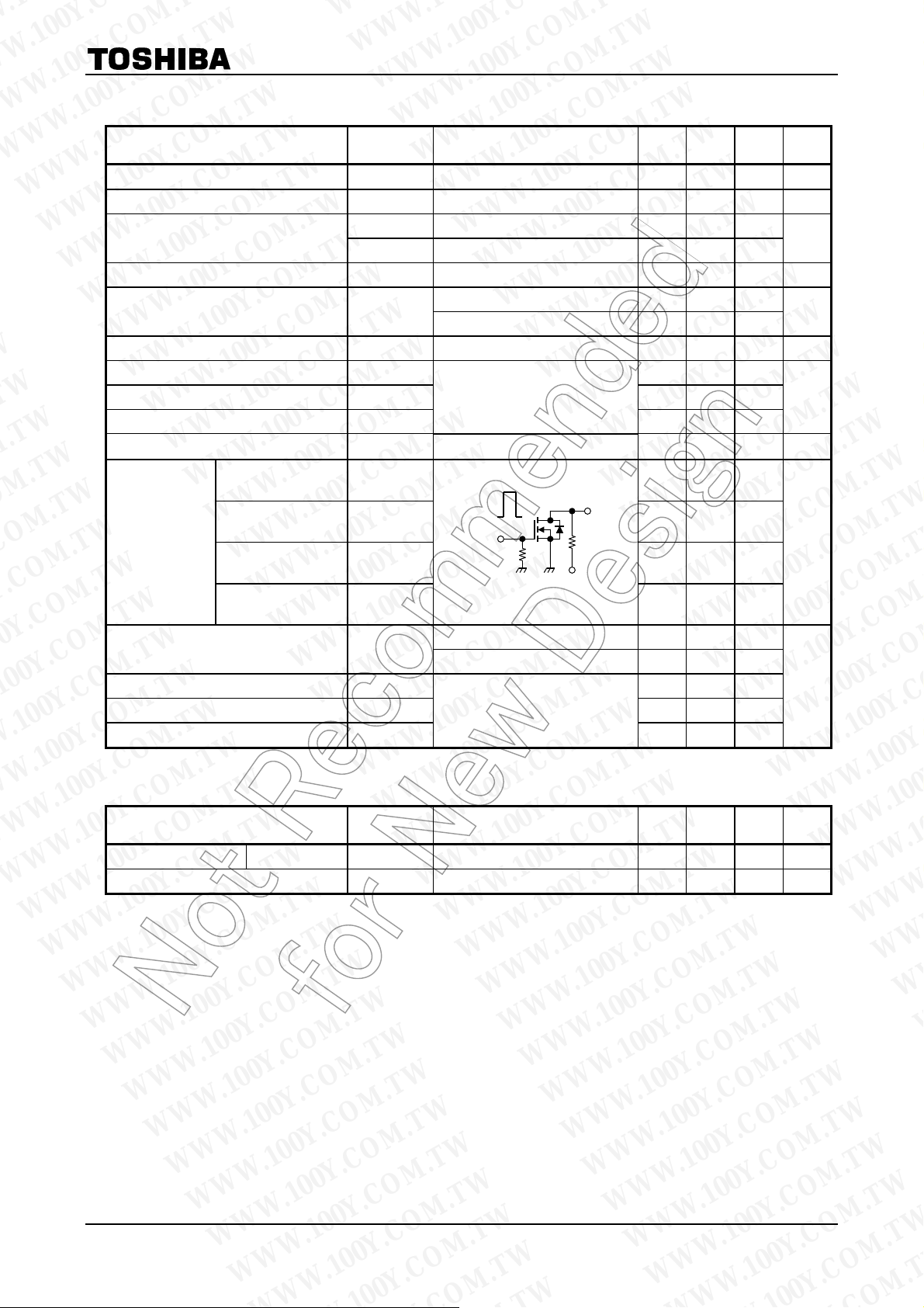
R
VDD ≈ 15 V
V
OUT
L
10 V
V
GS
0 V
Duty ≤ 1%, t
V
≈ 24 V, VGS = 10 V, ID = 24 A ⎯ 21 ⎯
DD
≈ 24 V, VGS = 5 V, ID = 24 A ⎯ 11 ⎯
V
DD
⎯ 4.7 ⎯
V
≈ 24 V, VGS = 10 V, ID = 24 A
DD
(Ta = 25°C)
⎯ 303 ⎯
⎯ 21 ⎯
⎯ 5.0 ⎯
V
mΩ
pF
ns
nC
Characteristic Symbol Test Condition Min Typ. Max Unit
Drain reverse current Pulse (Note 1) I
WWW.100Y.COM.TW WWW.100Y.COM.TW WWW.100Y.COM.TW
Forward voltage (diode) V
⎯ ⎯ ⎯ 72 A
DRP
IDR = 24 A, VGS = 0 V ⎯ ⎯ −1.2 V
DSF
WWW.100Y.COM.TW WWW.100Y.COM.TW WWW.100Y.COM.TW
WWW.100Y.COM.TW WWW.100Y.COM.TW WWW.100Y.COM.TW
WWW.100Y.COM.TW WWW.100Y.COM.TW WWW.100Y.COM.TW
WWW.100Y.COM.TW WWW.100Y.COM.TW WWW.100Y.COM.TW
WWW.100Y.COM.TW WWW.100Y.COM.TW WWW.100Y.COM.TW
WWW.100Y.COM.TW WWW.100Y.COM.TW WWW.100Y.COM.TW
WWW.100Y.COM.TW WWW.100Y.COM.TW WWW.100Y.COM.TW
WWW.100Y.COM.TW WWW.100Y.COM.TW WWW.100Y.COM.TW
WWW.100Y.COM.TW WWW.100Y.COM.TW WWW.100Y.COM.TW
WWW.100Y.COM.TW WWW.100Y.COM.TW WWW.100Y.COM.TW
3
2008-06-20
WWW.100Y.COM.TW WWW.100Y.COM.TW WWW.100Y.COM.TW
 Loading...