

TOSHIBA TPCA8028-H Datasheet

TPCA8028-H
A
TOSHIBA Field Effect Transistor Silicon N-Channel MOS Type (U-MOSⅥ-H)
TPCA8028-H
High-Efficiency DC/DC Converter Applications
Notebook PC Applications
Portable Equipment Applications
• Small footprint due to a small and thin package
• High-speed switching
• Small gate charge: Q
• Low drain-source ON-resistance: R
• High forward transfer admittance: |Y
• Low leakage current: I
• Enhancement mode: Vth = 1.3 to 2.3 V (VDS = 10 V, ID = 1 mA)
Absolute Maximum Ratings
Characteristic Symbol Rating Unit
Drain-source voltage
Drain-gate voltage (RGS = 20 kΩ)
Gate-source voltage
Drain current
Drain power dissipation (Tc=25℃) PD 45 W
Drain power dissipation (t = 10 s)
(Note 2a)
Drain power dissipation (t = 10 s)
(Note 2b)
Single-pulse avalanche energy
Avalanche current IAR 50 A
Repetitive avalanche energy
(Tc=25℃) (Note 4)
Channel temperature
Storage temperature range
Note: For Notes 1 to 4, refer to the next page.
= 20 nC (typ.)
SW
DS (ON)
= 10 μA (max) (VDS = 30 V)
DSS
(Ta = 25°C)
DC (Note 1) ID 50
Pulsed (Note 1) I
(Note 3)
= 2.0 mΩ (typ.)
| = 166 S (typ.)
fs
V
30 V
DSS
V
30 V
DGR
V
±20 V
GSS
150
DP
P
2.8 W
D
P
1.6 W
D
E
325 mJ
AS
E
4.03 mJ
AR
T
150 °C
ch
T
−55 to 150 °C
stg
A
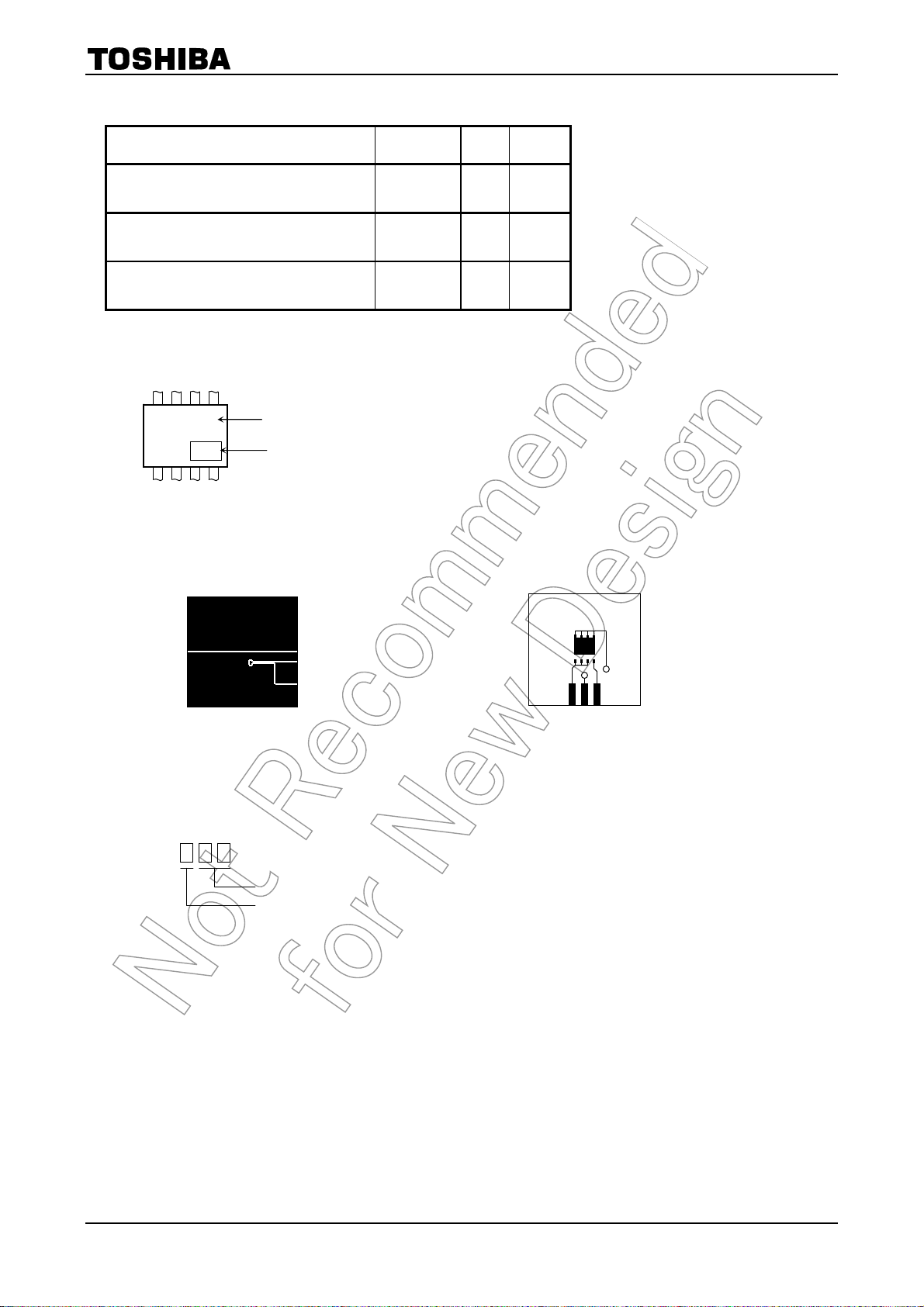
Unit: mm
0.5±0.1
8
6.0±0.3
5.0±0.2
1
0.95±0.05
S
1,2,3:SOURCE 4:GATE
5,6,7,8:DRAIN
5.0±0.2
0.05 S
1
0.6±0.1
4.25±0.2
0.05 M
5
0.15±0.05
4
0.595
A
0.166±0.05
1.1±0.2
4
3.5±0.2
58
0.8±0.1
0.4±0.1
1.27
JEDEC ―
JEITA ―
TOSHIBA 2-5Q1A
Weight: 0.069 g (typ.)
Circuit Configuration
8 6
1 2 3
7 5
4
Using continuously under heavy loads (e.g. the application of high
temperature/current/voltage and the significant change in temperature, etc.) may cause this product to decrease in the
reliability significantly even if the operating conditions (i.e. operating temperature/current/voltage, etc.) are within the
absolute maximum ratings. Please design the appropriate reliability upon reviewing the Toshiba Semiconductor Reliability
Handbook (“Handling Precautions”/“Derating Concept and Methods”) and individual reliability data (i.e. reliability test report
and estimated failure rate, etc).
This transistor is an electrostatic-sensitive device. Handle with care.
1
2008-01-22
Thermal Characteristics
Characteristic Symbol Max Unit
TPCA8028-H
Thermal resistance, channel to case
(Tc=25℃)
Thermal resistance, channel to ambient
(t = 10 s) (Note 2a)
Thermal resistance, channel to ambient
(t = 10 s) (Note 2b)
R
R
R
2.78 °C/W
th (ch-c)
44.6 °C/W
th (ch-a)
78.1 °C/W
th (ch-a)
Marking
(Note 5)
8028-H
※
Type TPCA
Lot No.
Note 1: Ensure that the channel temperature does not exceed 150°C.
Note 2: Device mounted on a glass-epoxy board
FR-4
25.4 × 25.4 × 0.8
(Unit: mm)
(a)
Note 3: V
= 24 V, Tch = 25°C (initial), L = 100 μH, RG = 25 Ω, IAR = 50 A
DD
Note 4: Repetitive rating: pulse width limited by maximum channel temperature
Note 5:
* Weekly code: (Three digits)
Week of manufacture
(01 for first week of year, continuing up to 52 or 53)
Year of manufacture
(The last digit of the calendar year)
FR-4
25.4 × 25.4 × 0.8
(Unit: mm)
(b)
2
2008-01-22
TPCA8028-H
∼
∼
∼
∼
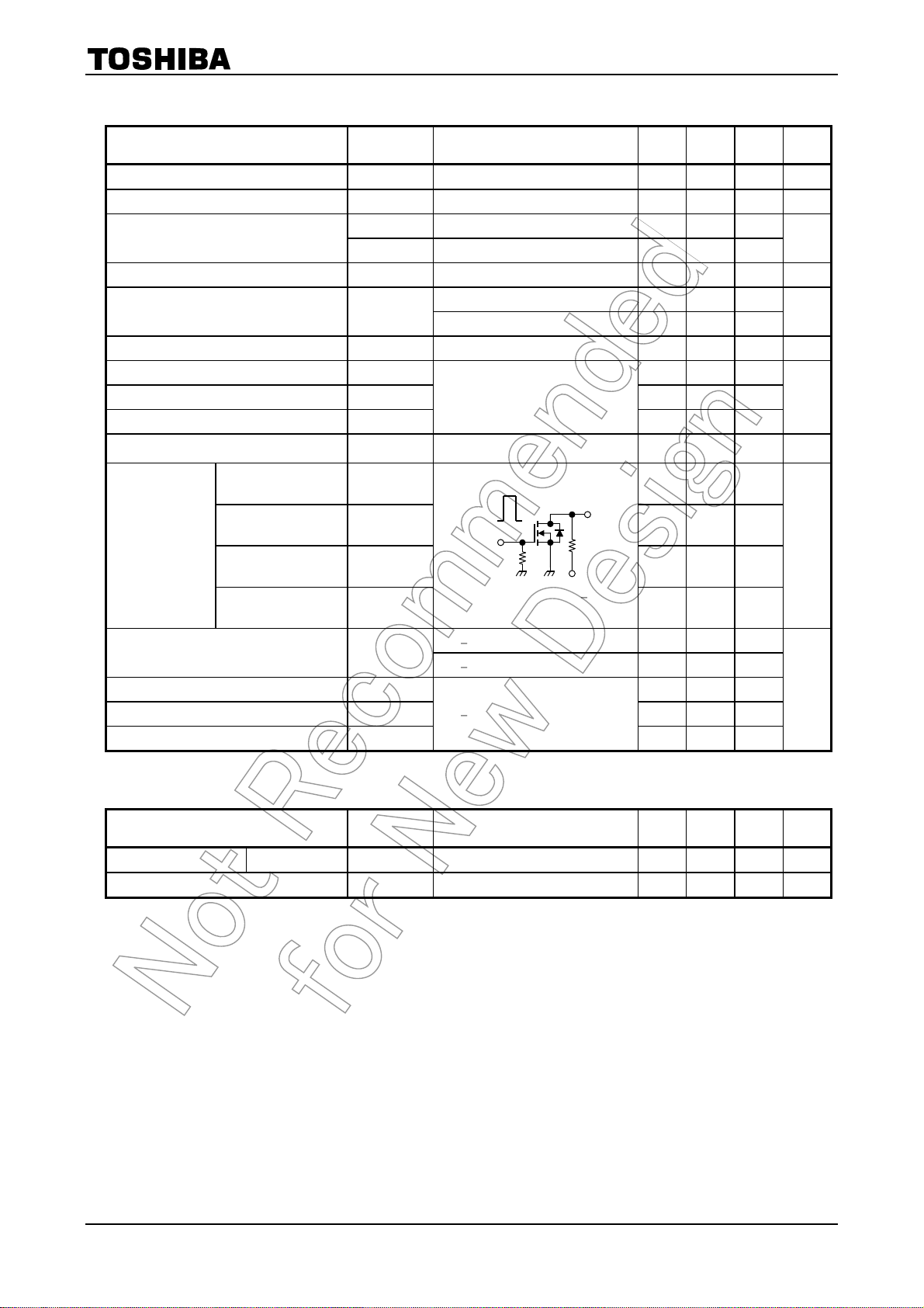
Electrical Characteristics
Characteristic Symbol Test Condition Min Typ. Max Unit
Gate leakage current I
Drain cutoff current I
Drain-source breakdown voltage
Gate threshold voltage Vth VDS = 10 V, ID = 1 mA 1.3 ⎯ 2.3 V
Drain-source ON-resistance R
Forward transfer admittance |Yfs| VDS = 10 V, ID = 25 A 83 166 ⎯ S
Input capacitance C
Reverse transfer capacitance C
Output capacitance C
Gate resistance Rg VDS = 10 V, VGS = 0 V, f = 1 MHz
Rise time tr ⎯ 5.0 ⎯
Turn-on time ton ⎯ 16 ⎯
Switching time
Fall time tf ⎯ 9.8 ⎯
Turn-off time t
Total gate charge
(gate-source plus gate-drain)
Gate-source charge 1 Q
Gate-drain (“Miller”) charge Qgd ⎯ 12 ⎯
Gate switch charge QSW
(Ta = 25°C)
VGS = ±20 V, VDS = 0 V ⎯ ⎯ ±100 nA
GSS
VDS = 30 V, VGS = 0 V ⎯ ⎯ 10 μA
DSS
V
(BR) DSSID
V
(BR) DSXID
DS (ON)
⎯ 6000 7800
iss
⎯ 380 610
rss
oss
off
Q
g
gs1
= 10 mA, VGS = 0 V 30 ⎯ ⎯
= 10 mA, VGS = −20 V 15 ⎯ ⎯
VGS = 4.5 V, ID = 25 A ⎯ 2.3 3.2
= 10 V, ID = 25 A ⎯ 2.0 2.8
V
GS
V
= 10 V, VGS = 0 V, f = 1 MHz
DS
4.7 Ω
= 10 μs
w
ID = 25A
V
DD
V
= 0.6Ω
L
R
15 V
OUT
10 V
V
GS
0 V
Duty ≤ 1%, t
V
24 V, VGS = 10 V, ID = 50 A ⎯ 88 ⎯
DD
V
24 V, VGS = 5 V, ID = 50 A ⎯ 46 ⎯
DD
⎯ 16 ⎯
V
24 V, VGS = 10 V, ID = 50 A
DD
⎯ 1100 ⎯
⎯ 1.0 1.5 Ω
⎯ 71 ⎯
⎯ 20 ⎯
Source-Drain Ratings and Characteristics
(Ta = 25°C)
V
mΩ
pF
ns
nC
Characteristic Symbol Test Condition Min Typ. Max Unit
Drain reverse current Pulse (Note 1) I
Forward voltage (diode) V
⎯ ⎯ ⎯ 150 A
DRP
IDR = 50 A, VGS = 0 V ⎯ ⎯ −1.2 V
DSF
3
2008-01-22
 Loading...