

查询TPC8201供应商
TOSHIBA Field Effect Transistor Silicon N Channel MOS Type (π−MOSVI)
TPC8201
TPC8201
Lithium Ion Battery Applications
Portable Equipment Applications
Notebook PCs
l Low drain−source ON resistance : R
DS (ON)
l High forward transfer admittance : |Y
l Low leakage current : I
= 10 µA (max) (VDS = 30 V)
DSS
l Enhancement−mode : Vth = 0.8~2.0 V (VDS = 10 V, ID = 1 mA)
Maximum Ratings
Characteristics Symbol Rating Unit
Drain-source voltage V
Drain-gate voltage (RGS = 20kΩ) V
Gate-source voltage V
Drain curren
Drain power
dissipation
(t = 10s)
(Note 2a)
Drain power
dissipation
(t = 10s)
(Note 2b)
Single pulse avalanche energy
(Note 4)
Avalanche current I
Repetitive avalanche energy
Single-device value at operation
(Note 2a, 3b, 5)
Channel temperature Tch 150 °C
Storage temperature range T
(Ta = 25°C)
DSS
DGR
GSS
D C (Note 1) I
Pulse (Note 1) I
Single-device
operation
(Note 3a)
Single-device value
at dual operation
Single-device
operation
(Note 3a)
Single-device value
at dual operation
(Note 3b)
(Note 3b)
P
P
P
P
DP
D (1)
D(2)
D (1)
D (2)
E
AR
E
AR
stg
= 37 mΩ (typ.)
| = 6 S (typ.)
fs
D
1.5
1.1
0.75
0.45
AS
30 V
30 V
±20 V
5
20
32.5 mJ
5 A
0.1 mJ
−55~150 °C
A
W
W
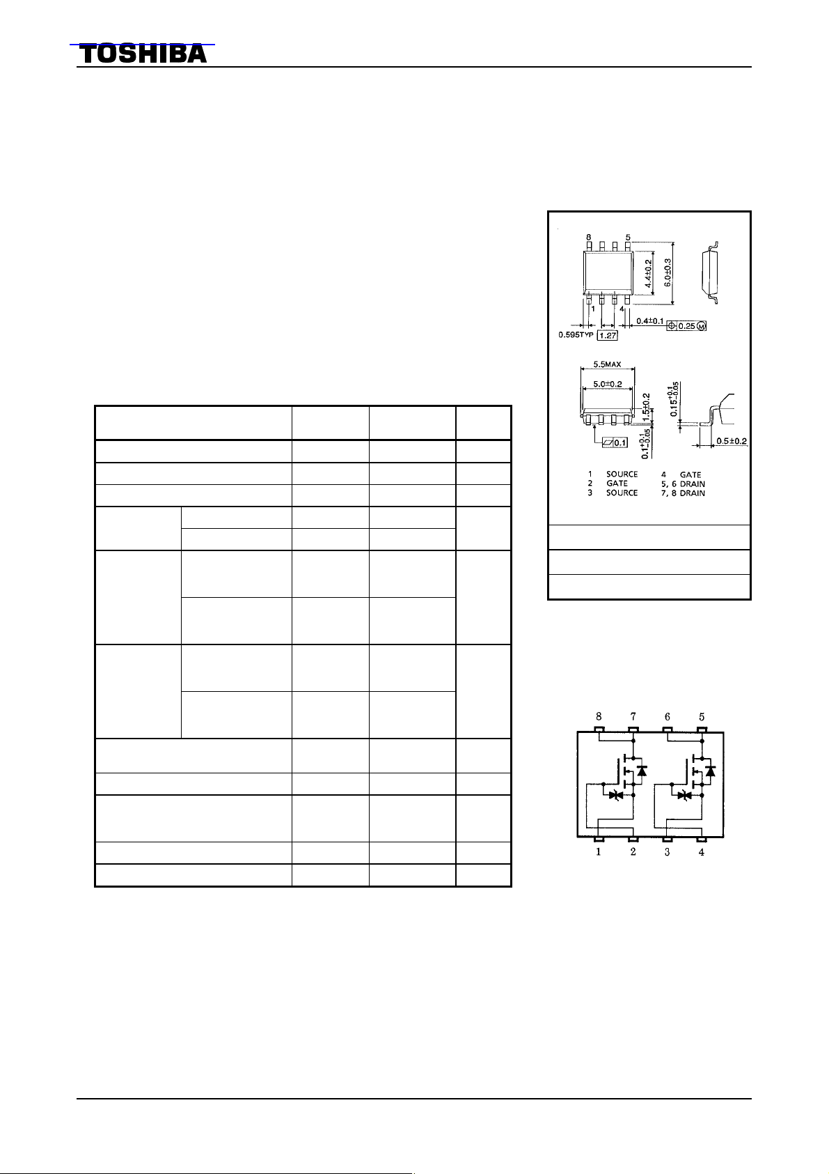
Unit: mm
JEDEC ―
JEITA ―
TOSHIBA 2-6J1E
Weight: 0.08 g (typ.)
Circuit Configuration
Note: For (Note 1), (Note 2a), (Note 2b), (Note 3a), (Note 3b), (Note 4) and (Note 5) please refer to the next page.
This transistor is an electrostatic sensitive device. Please handle with caution.
1
2003-02-20
Thermal Characteristics
Characteristics Symbol Max Unit
TPC8201
Thermal resistance, channel to ambient
(t = 10s) (Note 2a)
Thermal resistance, channel to ambient
(t = 10s) (Note 2b)
Single-device operation
(Note 3a)
Single-device value at
dual operation
(Note 3b)
Single-device operation
(Note 3a)
Single-device value at
dual operation
(Note 3b)
R
th (ch-a) (1)
R
th (ch-a) (2)
R
th (ch-a) (1)
R
th (ch-a) (2)
83.3
114
°C/W
167
278
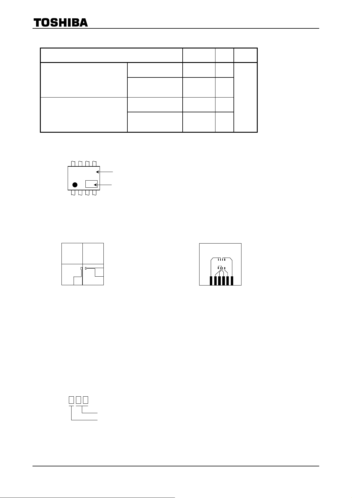
Marking
(Note 6)
TPC8201
※
Type
Lot No.
Note 1: Please use devices on condition that the channel temperature is below 150°C.
Note 2:
a) Device mounted on a glass-epoxy board (a) b) Device mounted on a glass-epoxy board (b)
FR-4
25.4 × 25.4 × 0.8
(Unit: mm)
(a)
(b)
Note 3:
a) The power dissipation and thermal resistance values are shown for a single device
(During single-device operation, power is only applied to one device.).
b) The power dissipation and thermal resistance values are shown for a single device
(During dual operation, power is evenly applied to both devices.).
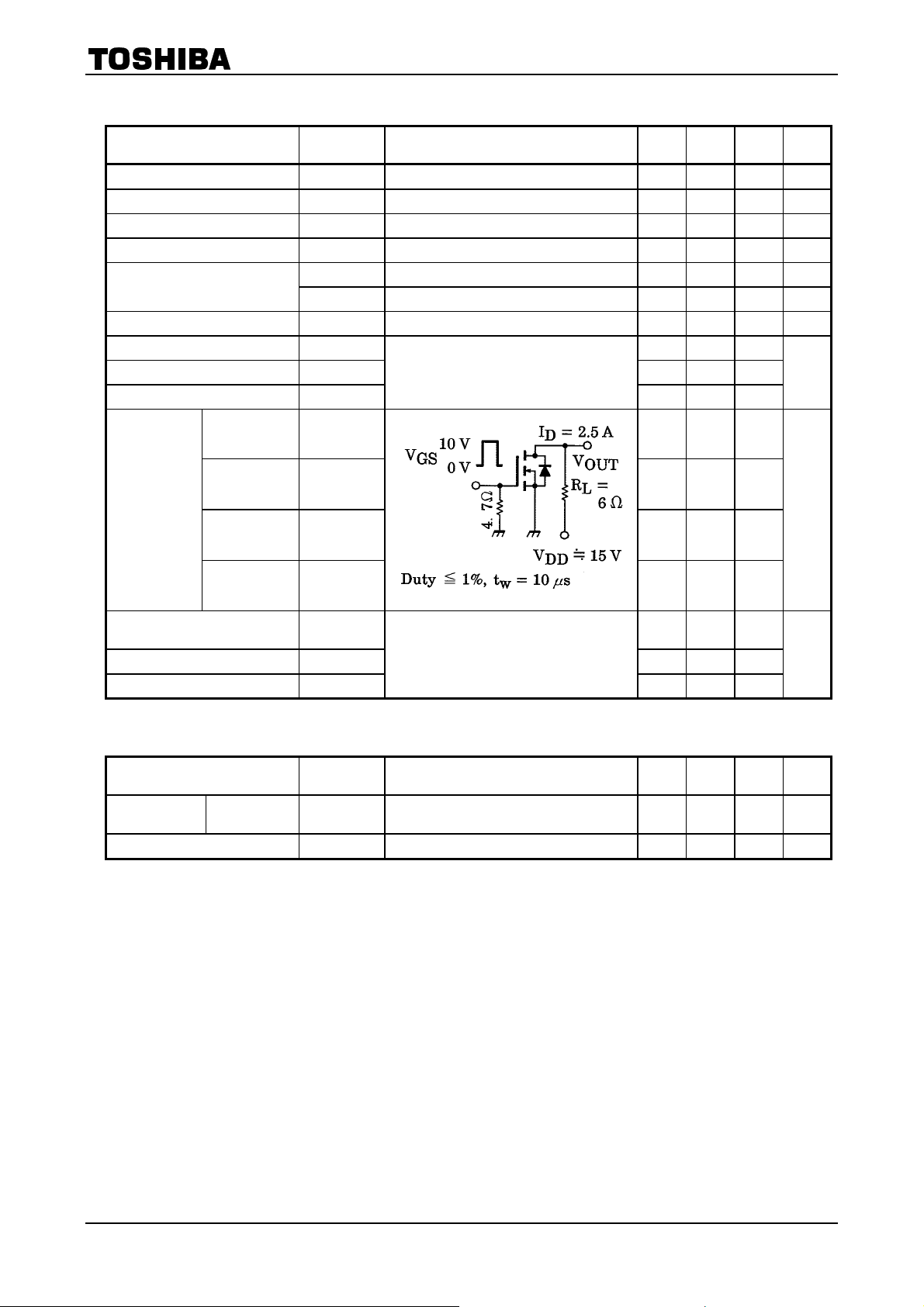
Note 4: V
= 16 V, Tch = 25°C (initial), L = 1.0 mH, RG = 25 Ω, IAR = 6 A
DD
Note 5: Repetitive rating; pulse width limited by maximum channel temperature.
Note 6: ● on lower right of the marking indicates Pin 1.
※ Weekly code:(Three digits)
Week of manufacture
(01 for first week of year, continues up to 52 or 53)
FR-4
25.4 × 25.4 × 0.8
(Unit: mm)
Year of manufacture
(One low-order digits of calendar year)
2
2003-02-20
TPC8201
Electrical Characteristics
(Ta = 25°C)
Characteristics Symbol Test Condition Min Typ. Max Unit
Gate leakage current I
Drain cut−off current I
Drain−source breakdown voltage V
(BR) DSS
Gate threshold voltage V
R
Drain−source ON resistance
DS (ON)
R
DS (ON)
GSS
DSS
th
VGS = ±16 V, VDS = 0 V — — ±10 µA
VDS = 30 V, VGS = 0 V — — 10 µA
ID = 10 mA, VGS = 0 V 30 — — V
VDS = 10 V, ID = 1 mA 0.8 — 2.0 V
VGS = 4 V, ID = 2.5 A — 58 80 mΩ
VGS = 10 V, ID = 2.5 A — 37 50 mΩ
Forward transfer admittance |Yfs| VDS = 10 V, ID = 2.5 A 3 6 — S
Input capacitance C
Reverse transfer capacitance C
Output capacitance C
— 475 —
iss
VDS = 10 V, VGS = 0 V, f = 1 MHz
— 85 —
rss
oss
— 270 —
Rise time tr — 10 —
Turn−on time ton — 16 —
Switching time
Fall time tf — 13 —
pF
ns
Turn−off time t
Total gate charge (Gate−source
plus gate−drain)
Gate−source charge Qgs — 11 —
Gate−drain (“miller”) charge Qgd
— 70 —
off
Q
— 16 —
g
V
≈ 24 V, VGS = 10 V, ID = 5 A
DD
nC
— 5 —
Source−Drain Ratings and Characteristics
Characteristics Symbol Test Condition Min Typ. Max Unit
Drain reverse
current
Forward voltage (diode) V
Pulse (Note 1) I
DRP
DSF
IDR = 5 A, VGS = 0 V — — −1.2 V
(Ta = 25°C)
— — — 20 A
3
2003-02-20
 Loading...