


查询TOTR370M-IRV1A供应商
Optical Communication Devices
September 2001
10Gb/s Optical Transponder
TOTR370M-IR Series
APPLICATION
SONET / SDH (OC-192 / STM-64) applications
•
FEATURES
10 Gb/s optical transceiver with 16 Channel Mux and DeMux
•
Differential LVDS 622 Mb/s data and 622 MHz clock interface
•
Optical input power range: –17 dBm (typ) to 0 dBm (@ BER = 10
•
Optical output power range: –4 dBm (typ) to –2 dBm /–0.5 dBm to +1.5dBm
•
Target distance: 25 km/40 km
•
Tc: 0 ˚C to 70 ˚C
•
Power supply: +5.0 V, +3.3 V and −5.2 V
•
Package size: 114 x 88.9 x 13.4 mm
•
–12
)
TOTR370M-IR Series
TOTR370M-IR Series
TOTR370M-IR Series
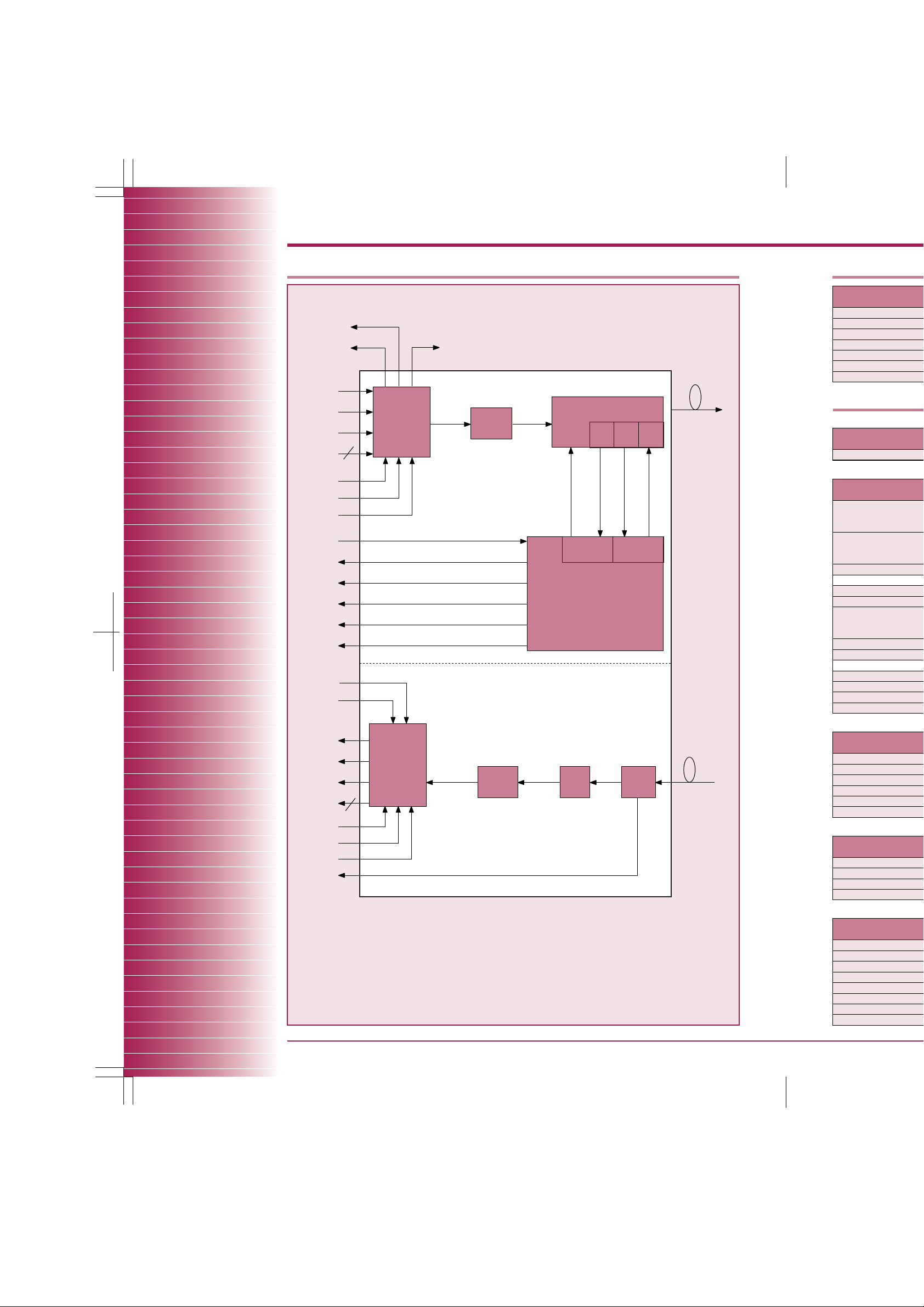
BLOCK DIAGRAM
TxREFSEL
TxRATESEL
TxRESET
TxPHSADJ0/1
LsENABLE
LsBIASALM
LsTEMPALM
LsBIASMON
LsPOWMON
LsTEMPMON
RxRESET
RxRATESEL
RxLOCKERR
RxMCLK
RxPOCLK
RxDout
RxREFCLK
RxREFSEL
RxMCLKSEL
RxPOWMON
TxREFCLK
TxPICLK
622MHz
622Mb/s
622MHz
622Mb/s
TxDin
16
TxMCLK
TxPCLK
TxLOCKERR
10 Gb/s
10 Gb/s
Transmitter Side
Optical Fiber
Output
Optical Fiber
Input
Receiver Side
EML
Control Circuits
PD
TIA PIN PD
APC
APC: Automatic Power Control
ATC: Automatic Temperature Control
TEC: Thermo-Electric Cooler
TIA: Transimpedance Amplifier
ATC
TEC
Thermistor
Limiting
Amplifier
Timing
Generation
16:1 Mux
Clook and Data
Recovery
1:16 DeMux
Modulator
Driver
16
ABSOLUTE MA
It
Storage temperature
Input data signal volt
Input optical peak po
Input optical average
Positive supply 1 vol
Positive supply 2 vol
Negative supply volta
It
Operating case temp
Operating Tempe
Electrical Power S
It
It
ELECTRICAL A
Optical Character
Optical fiber output p
Target distance
Dispersion
Operating wavelengt
Transmitter
Spectral Width (@ 20
Side mode Suppress
Extinction ratio
Optical return loss
Receiver
Sensitivity (@ BER =
Overload
Optical return loss
Optical path penalty
Positive supply 1 vol
Positive supply 1 cur
Positive supply 2 vol
Positive supply 2 cur
Negative supply volta
Negative supply curr
Electrical Input an
It
Alam output high lev
Alam output low leve
Control input high lev
Control intput low lev
Electrical Input an
It
Input power monitor vol
Normalized laser power
50% variation of laser p
Laser disable mode
Laser monitor bias vo
Laser monitor bias of
Normalized laser temper
Normalized laser temper

T
v
.
ABSOLUTE MAXIMUM RATINGS
C
C
C
C
C
C
C
C
C
C
C
C
C
C
C
C
C
C
C
C
C
C
C
C
C
C
C
C
C
C
DIMENSIONAL OU
Optical Fiber
Output
10 Gb/s
Optical Fiber
Input
10 Gb/s
Item
Storage temperature
Input data signal voltage
Input optical peak power
Input optical average power
Positive supply 1 voltage
Positive supply 2 voltage
Negative supply voltage
Ratings
−40 to +85
GND–0.5 to V
+3
0
0 to 6
–0.5 to +3.8
–6.5 to +0.3
DD
ELECTRICAL AND OPTICAL CHARACTERISTICS
Operating Temperature
Item
Operating case temperature range
Optical Characteristics
Item
TOTR370M-IRV1A
Target distance
Dispersion
Operating wavelength range
Transmitter
Spectral Width (@ 20 dB down)
Side mode Suppression Ratio
Optical fiber output power
Extinction ratio
Optical return loss
Receiver
Sensitivity (@ BER = 10
Overload
Optical return loss
Optical path penalty (@ Target distance)
TOTR370M-IRV1B
TOTR370M-IRV1C
TOTR370M-IRV1A
TOTR370M-IRV1B
TOTR370M-IRV1C
TOTR370M-IRV1A
TOTR370M-IRV1B
TOTR370M-IRV1C
–12
)
Electrical Power Supplies
Item
Positive supply 1 voltage
Positive supply 1 current
Positive supply 2 voltage
Positive supply 2 current
Negative supply voltage
Negative supply current
Electrical Input and Output Signals (Digital Signal Characteristics)
Item
Alam output high level
Alam output low level
Control input high level
Control intput low level
Electrical Input and Output Signals (Analog Signal Characteristics)
Item
Input power monitor voltage slope for PIN
Normalized laser power monitor voltage
50% variation of laser power (linear slope)
Laser disable mode
Laser monitor bias voltage slope
Laser monitor bias offset voltage
Normalized laser temperature monitor voltage
Normalized laser temperature monitor slope
Min Typ. Max
0 – +70
Min Typ. Max
−
–
–
–
–
–
1530
–
30
–4.0
–0.5
–4.0
8.2
30
–
0
27
–
Symbol Typ. Max
V
CC
I
CC
V
DD
I
DD
V
EE
I
EE
Min
+4.75
+3.135
–5.4
25
40
40
–
–
–
–
–
–
–
–
–
–
–
–17
–
–
–
–
–
–
Min Typ. Max
VDD–0.5
GND
–1.0
V
DD
GND
Symbol Typ. Max
RxPOWMON
LsPOWMON
–
–
LsBIASMON
–
LsTEMPMON
–
Min
0.8
0.44
–20
17.8
–20
–
–
–
–
–
–
–
+0.5
+5.0
–
+3.3
–
–5.2
–
–
0.5
0.25
–
20
–
2.5
–40
–
–
–
500
800
800
1565
1.0
–
–2.0
+1.5
–2.0
–
–
–14
–
–
2
V
DD
0.5
V
DD
1.0
+5.25
250
+3.465
2500
–5.0
500
1.26
0.56
–
20
22.5
20
–
–
Unit
˚C
V
dBm
dBm
V
V
V
Unit
˚C
Unit
km
ps/nm
nm
nm
dB
dBm
dB
dB
dBm
dBm
dB
dB
Unit
mA
mA
mA
Unit
V
V
V
V
Unit
V/mW
mV
mV/mA
mV
mV/˚C
Receiver
88
Top
Pin Map Overview
KJ
+5.0V
1
+5.0V
2
RxRATESEL
3
+3.3V
4
+3.3V
5
RxRESET
6
V
V
V
V
V
V
7
8
9
10
11
12
13
14
15
16
17
18
19
20
21
22
23
24
25
26
27
28
29
30
NC
NC
NC
-5.2V
-5.2V
NC
-5.2V
-5.2V
NC
+5.0V
+5.0V
NC
+3.3V
+3.3V
TxRATESEL
+3.3V
+3.3V
TxRESET
-5.2V
-5.2V
NC
-5.2V
-5.2V
NC
N
N
N
N
N
N
N
N
N
N
N
N
N
N
N
N
N
N
N
N
N
N
N
N
N
N
N
N
N
N

DIMENSIONAL OUTLINE AND PIN ASSIGNMENT
Unit
˚C
V
dBm
dBm
V
V
V
Unit
˚C
Unit
km
ps/nm
nm
nm
dB
dBm
Receiver Transmitter
88.9
114.3
13.4
0.5
45.7
(27.7)
12.69.4
29.9
K30
21.25
Bottom viewSide viewTop view
30.0 Max
A30 A1
21.25
46.7
29.9
K1
(24.5)
4-M2.5 (3mm deep)
300 pin FCI
Meg Array connector
21.12
(Unit: mm)
12.1
Max
+5.25
250
+3.465
2500
–5.0
500
Max
1.26
0.56
–
20
22.5
20
–
–
dB
dB
dBm
dBm
dB
dB
Unit
V
mA
V
mA
V
mA
Unit
V
V
V
V
Unit
V/mW
V
V
mV
mV/mA
mV
V
mV/˚C
Pin Map Overview
KJHGF E DC B A
+5.0V
1
+5.0V
2
RxRATESEL
3
+3.3V
4
+3.3V
5
RxRESET
6
7
8
9
10
11
12
13
14
15
16
17
18
19
20
21
22
23
24
25
26
27
28
29
30
NC
NC
NC
-5.2V
-5.2V
NC
-5.2V
-5.2V
NC
+5.0V
+5.0V
NC
+3.3V
+3.3V
TxRATESEL
+3.3V
+3.3V
TxRESET
-5.2V
-5.2V
NC
-5.2V
-5.2V
NC
NC
NC
NC
NC
NC
NC
NC
NC
NC
NC
NC
NC
NC
NC
NC
NC
NC
NC
NC
NC
NC
NC
NC
NC
NC
NC
NC
NC
NC
NC
GND
GND
NC
GND
GND
NC
GND
GND
NC
GND
GND
NC
GND
GND
NC
GND
GND
NC
GND
GND
NC
GND
GND
NC
GND
GND
NC
GND
GND
NC
RxDout12P
RxDout12N
GND
RxDout13P
RxDout13N
GND
RxDout14P
RxDout14N
GND
RxDout15P
RxDout15N
GND
NC
NC
GND
TxDin12P
TxDin12N
GND
TxDin13P
TxDin13N
GND
TxDin14P
TxDin14N
GND
TxDin15P
TxDin15N
GND
TxPICLKP
TxPICLKN
GND
NC
NC
RxPOWMON
+3.3V
+3.3V
NC
+3.3V
+3.3V
NC
-5.2V
-5.2V
NC
-5.2V
-5.2V
RxREFSEL
NC
NC
LsBIASMON
+3.3V
+3.3V
LsENABLE
+3.3V
+3.3V
LsBIASALM
-5.2V
-5.2V
LsTEMPALM
-5.2V
-5.2V
TxREFSEL
RxDout8P
RxDout8N
GND
RxDout9P
RxDout9N
GND
RxDout10P
RxDout10N
GND
RxDout11P
RxDout11N
GND
RxPOCLKP
RxPOCLKN
GND
TxDin8P
TxDin8N
GND
TxDin9P
TxDin9N
GND
TxDin10P
TxDin10N
GND
RxDin11P
RxDin11N
GND
TxPCLKP
TxPCLKN
GND
GND
GND
NC
GND
GND
NC
GND
GND
NC
GND
GND
NC
GND
GND
NC
GND
GND
LsPOWMON
GND
GND
LsTEMPMON
GND
GND
TxPHSADJ0
GND
GND
TxPHSADJ1
GND
GND
NC
RxDout4P
RxDout4N
GND
RxDout5P
RxDout5N
GND
RxDout6P
RxDout6N
GND
RxDout7P
RxDout7N
GND
RxMCLKP
RxMCLKN
GND
TxDin4P
TxDin4N
GND
TxDin5P
TxDin5N
GND
TxDin6P
TxDin6N
GND
RxDin7P
RxDin7N
GND
TxMCLKP
TxMCLKN
GND
GND
GND
NC
GND
GND
NC
GND
GND
NC
GND
GND
RxMCLKSEL
GND
GND
RxLOCKERR
GND
GND
NC
GND
GND
NC
GND
GND
NC
GND
GND
NC
GND
GND
TxLOCKERR
RxDout0P
RxDout0N
GND
RxDout1P
RxDout1N
GND
RxDout2P
RxDout2N
GND
RxDout3P
RxDout3N
GND
RxREFCLKP
RxREFCLKN
GND
TxDin0P
TxDin0N
GND
TxDin1P
TxDin1N
GND
TxDin2P
TxDin2N
GND
TxDin3P
TxDin3N
GND
TxREFCLKP
TxREFCLKN
GND

PRECAUTIONS
(a) Power supply: Transient electric spike may cause a damage to the laser, the photodiode or IC chips.
A surge-free power supply and a slow starter circuit should be used.
To avoid causing an electrical surge, pins should not be connected or disconnected on the test fixture
before turning power off .
(b) The product should be grounded for obtaining the performance.
(c) Safety: The laser emits invisible light harmful to the human eyes. Direct viewing should be avoided.
Input Controls Truth Tables
Output Alarms Truth Tables
RxRATESEL (Pin # K3)
0
1 or NC
FEC rate of 10.664Gb/s and 10.709Gb/s selected
normal SONET rate of 9.953Gb/s or Ethernet rate of 10.3Gb/s selected
TxRATESEL (Pin # K21)
0
1 or NC
FEC rate of 10.664Gb/s and 10.709Gb/s selected
normal SONET rate of 9.953Gb/s or Ethernet rate of 10.3Gb/s selected
RxRESET (Pin # K6)
0
1 or NC
asynchronous DeMux system reset
normal operation
TxRESET (Pin # K24)
0
1 or NC
asynchronous Mux system reset
normal operation
LsENABLE (Pin # F21)
0 or NC
1
normal operation
laser disable
LsBIASALM (Pin # F24)
0
1
laser bias alarm active
normal operation
LsTEMPALM (Pin # F27)
0
1
laser temperature alarm active
normal operation
RxLOCKERR (Pin # B15)
0
1
indicates loss of PLL lock
normal operation
TxLOCKERR (Pin # B30)
0
1
indicates loss of PLL lock
normal operation
TxPHSADJ1 (Pin # D27)
0 or NC
0 or NC
1
1
TxPHSADJ0 (Pin # D24)
0 or NC
1
0 or NC
1
adjusts the phase of the TxPCLK by 0deg
adjusts the phase of the TxPCLK by 90deg
adjusts the phase of the TxPCLK by 180deg
adjusts the phase of the TxPCLK by 270deg
RxREFSEL (Pin # F15)
0
1 or NC
selects an RxREFCLK frequency of 155MHz
selects an RxREFCLK frequency of 622MHz
RxMCLKSEL (Pin # B12)
0
1 or NC
selects an RxMCLK frequency of 155MHz
selects an RxMCLK frequency of 622MHz
TxREFSEL (Pin # F30)
0
1 or NC
selects a TxREFCLK frequency of 155MHz
selects a TxREFCLK frequency of 622MHz
3697C-0103 PC-D5

©2001 TOSHIBA CORPORATION
Printed in Japan
Website: http://www.semicon.toshiba.co.jp/eng/index.html
010126 (X)
Toshiba Electronics Europe GmbH
Düsseldorf Head Office
Hansaallee 181, D-40549 Düsseldorf
Germany
Tel: (0211)5296-0 Fax: (0211)5296-400
Toshiba Electronics Italiana S.R.L.
Centro Direzionale Colleoni
Palazzo Perseo Ingr. 2-Piano 6,
Via Paracelso n.12,
1-20041 Agrate Brianza Milan, Italy
Tel: (039)68701 Fax:(039)6870205
Toshiba Electronics(UK) Limited
Riverside Way, Camberley Surrey,
GU15 3YA, U.K.
Tel: (01276)69-4600 Fax: (01276)69-4800
Toshiba Electronics Scandinavia AB
Gustavslundsvägen 12, 2nd Floor
S-161 15 Bromma, Sweden
Tel: (08)704-0900 Fax: (08)80-8459
Toshiba Electronics Asia, Ltd.
Hong Kong Head Office
Level 11, Top Glory Insurance Building, Grand Century
Place, No.193, Prince Edward Road West,
Mong Kok, Kowloon, Hong Kong
Tel: 2375-6111 Fax: 2375-0969
Beijing Office
Rm 714, Beijing Fortune Building,
No.5 Dong San Huan Bei-Lu, Chao Yang District,
Beijing, 100004, China
Tel: (010)6590-8795 Fax: (010)6590-8791
Toshiba Electronics Korea
Corporation
Seoul Head Office
14/F, KEC B/D, 257-7 Yangjae-Dong,
Seocho-ku, Seoul, Korea
Tel: (02)589-4334 Fax: (02)589-4302
Toshiba Technology Development
(Shanghai) Co., Ltd.
23F, Shanghai Senmao International Building, 101
Yin Cheng East Road, Pudong New Area, Shanghai,
200120, China
Tel: (021)6841-0666 Fax: (021)6841-5002
Toshiba Electronics Taiwan
Corporation
Taipei Head Office
17F, Union Enterprise Plaza Bldg. 109
Min Sheng East Rd., Section 3, 0446 Taipei,
Taiwan
Tel: (02)514-9988 Fax: (02)514-7892
Toshiba America
Electronic Components, Inc.
Headquarters-Irvine, CA
9775 Toledo Way, Irvine, CA 92618, U.S.A.
Tel: (949)455-2000 Fax: (949)859-3963
Deerfield, IL(Chicago)
One Pkwy., North, Suite 500, Deerfield,
IL 60015-2547, U.S.A.
Tel: (847)945-1500 Fax: (847)945-1044
Edison, NJ
2035 Lincoln Hwy. Ste. #3000, Edison
NJ 08817, U.S.A.
Tel: (732)248-8070 Fax: (732)248-8030
Raleigh, NC
5511 Capitol Center Dr., #114,
Raleigh, NC 27606, U.S.A.
Tel: (919)859-2800 Fax: (919)859-2898
Richardson, TX(Dallas)
777 East Campbell Rd., Suite 650, Richardson,
TX 75081, U.S.A.
Tel: (972)480-0470 Fax: (972)235-4114
Wakefield, MA(Boston)
401 Edgewater Place, Suite #360, Wakefield,
MA 01880-6229, U.S.A.
Tel: (781)224-0074 Fax: (781)224-1095
The information contained herein is subject to change without notice.
The information contained herein is presented only as a guide for the applications of our products.
No responsibility is assumed by TOSHIBA for any infringements of patents or other rights of the third parties which may result
from its use. No license is granted by implication or otherwise under any patent or patent rights of TOSHIBA or others.
TOSHIBA is continually working to improve the quality and reliability of its products. Nevertheless, semiconductor devices in
general can malfunction or fail due to their inherent electrical sensitivity and vulnerability to physical stress. It is the
responsibility of the buyer, when utilizing TOSHIBA products, to comply with the standards of safety in making a safe design for
the entire system, and to avoid situations in which a malfunction or failure of such TOSHIBA products could cause loss of
human life, bodily injury or damage to property. In developing your designs, please ensure that TOSHIBA products are used
within specified operating ranges as set forth in the most recent TOSHIBA products specifications. Also, please keep in mind
the precautions and conditions set forth in the "Handling Guide for Semiconductor Devices," or "TOSHIBA Semiconductor
Reliability Handbook" etc..
The Toshiba products listed in this document are intended for usage in general electronics applications (computer, personal
equipment, office equipment, measuring equipment, industrial robotics, domestic appliances, etc.).
These Toshiba products are neither intended nor warranted for usage in equipment that requires extraordinarily high quality and/or
reliability or a malfunction or failure of which may cause loss of human life or bodily injury ("Unintended Usage"). Unintended Usage
include atomic energy control instruments, airplane or spaceship instruments, transportation instruments, traffic signal instruments,
combustion control instruments, medical instruments, all types of safety devices, etc.. Unintended Usage of Toshiba products listed
in this document shall be made at the customerís own risk.
The products described in this document are subject to the foreign exchange and foreign trade laws.
Gallium arsenide (GaAs) is a substance used in some of the products described in this documents. GaAs dust and fumes are toxic. Do not break, cut or pulverize the products, or use chemicals to dissolve them.
When disposing of the products, follow the appropriate regulations. Do not dispose of the products with other industrial waste or with domestic garbage.
Electronic Devices Sales & Marketing Division
1-1, Shibaura 1-chome, Minato-ku, Tokyo, 105-8001, Japan
Tel: +81-3-3457-3405 Fax: +81-3-5444-9431
OVERSEAS SUBSIDIARIES AND AFFILIATES
 Loading...