

TL(RK,RMK,SK,OK,YK)1100C(T11)
TOSHIBA LED Lamps
TLRK1100C(T11), TLRMK1100C(T11), TLSK1100C(T11),
TLOK1100C(T11), TLYK1100C(T11)
Panel Circuit Indicators
• Surface-mount devices
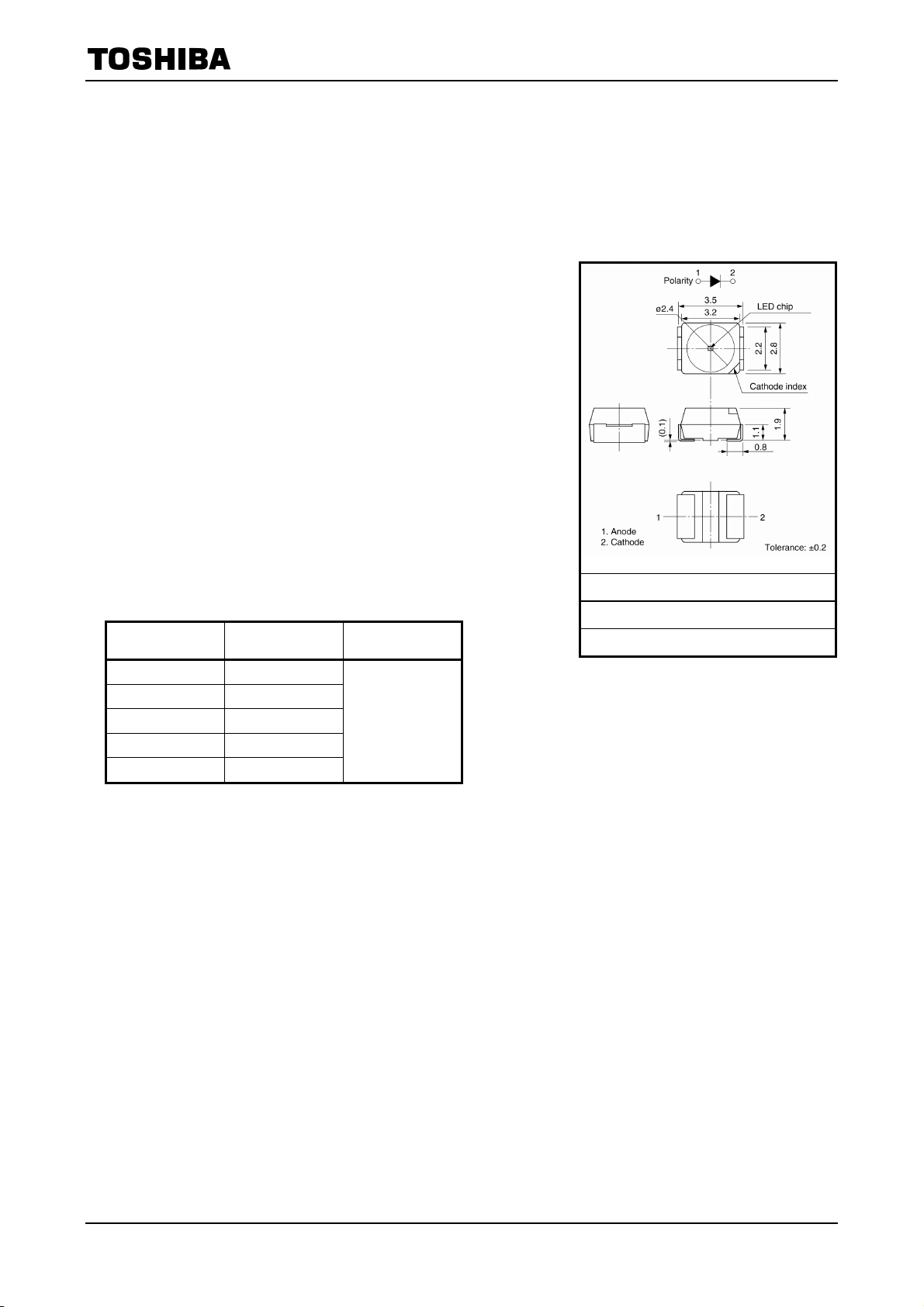
• 3.2 (L) mm × 2.8 (W) mm × 1.9 (H) mm
• Flat-top type
• InGaAℓP LEDs
• High luminous intensity
• Low drive current, high-intensity light emission
• Colors: red, orange, yellow
• Applications: automotive use, message signboards, backlighting
etc.
• Standard embossed tape packing: T11 (2000/reel)
8-mm tape reel
Color and Material
Part Number Color Material
JEDEC ―
JEITA ―
TOSHIBA 4-3R1
Unit: mm
TLRK1100C Red
TLRMK1100C Red
TLSK1100C Red
TLOK1100C Orange
TLYK1100C Yellow
Weight: 0.035 g (typ.)
InGaAℓP
1
2008-04-14
TL(RK,RMK,SK,OK,YK)1100C(T11)
Absolute Maximum Ratings
Forward Current
(mA)
Product Name
TLRK1100C
TLRMK1100C
TLSK1100C
TLOK1100C
TLYK1100C
I
F
Please see Note 1
30 4 75 −40 to 100 −40 to 100
(Ta = 25°C)
Reverse Voltage
Power Dissipation
V
R
(V)
PD (mW)
Operation
Temperature
T
(°C)
opr
Temperature
Note: Using continuously under heavy loads (e.g. the application of high temperature/current/voltage and the
significant change in temperature, etc.) may cause this product to decrease in the reliability significantly even
if the operating conditions (i.e. operating temperature/current/voltage, etc.) are within the absolute maximum
ratings.
Please design the appropriate reliability upon reviewing the Toshiba Semiconductor Reliability Handbook
(“Handling Precautions”/“Derating Concept and Methods”) and individual reliability data (i.e. reliability test
report and estimated failure rate, etc).
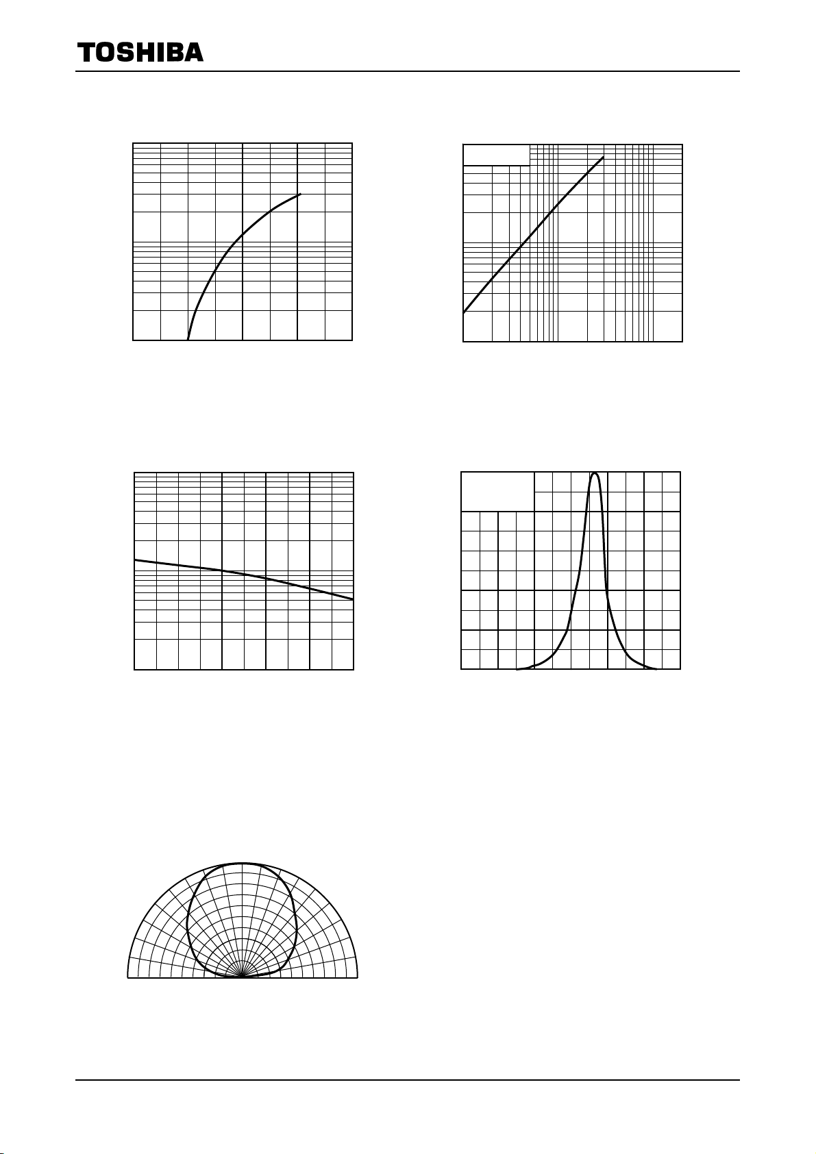
Note 1: Forward current derating
50
I
F
– Ta
40
(mA)
F
30
20
10
Allowable forward current I
0
0 20 40 60 80 100 120
Ambient temperature Ta (°C))
Electrical Characteristics
(Ta = 25°C)
Storage
T
(°C)
stg
Product Name
TLRK1100C 1.8 2.1 2.5
TLRMK1100C 1.8 2.1 2.5
TLSK1100C 1.8 2.1 2.5
TLOK1100C 1.8 2.1 2.5
TLYK1100C 1.8 2.2 2.5
Unit V mA μA V
Forward Voltage VF
Min Typ. Max I
Reverse Current
I
R
Max VR
F
20 10 4
2
2008-04-14
TL(RK,RMK,SK,OK,YK)1100C(T11)
Optical Characteristics–1
Product Name
Min Typ. Max I
TLRK1100C 100 300 500 20 RA / SA / TA
TLRMK1100C 160 400 800 20 SA / TA / UA
TLSK1100C 250 500 1250 20 TA / UA / VA
TLOK1100C 250 500 1250 20 TA / UA / VA
TLYK1100C 160 400 800 20 SA / TA / UA
Unit mcd mcd mcd mA ⎯
(Ta = 25°C)
Luminous Intensity IV
Available Iv rank
Please see Note 2
F
Note 2: The specification on the above table is used for Iv classification of LEDs in Toshiba facility.
Each reel includes the same rank LEDs. Let the delivery ratio of each rank be unquestioned.
Rank
RA 100 200
SA 160 320
TA 250 500
UA 400 800
VA 630 1250
Unit mcd mcd
Luminous Intensity IV
Min Max
Optical Characteristics–2
(Ta = 25°C)
Product Name
TLRK1100C ⎯ 644 ⎯ 14 624 630 638
TLRMK1100C ⎯ 636 ⎯ 14 620 626 634
TLSK1100C ⎯ 623 ⎯ 14 607 613 621
TLOK1100C ⎯ 612 ⎯ 14 599 605 613
TLYK1100C ⎯ 592 ⎯ 13 583 590 595
Unit nm nm nm mA
Peak Emission
Wavelength λ
Min Typ. Max Typ. Min Typ. Max
Emission Spectrum
p
Δλ Dominant Wavelength λ
d
I
F
20
The cautions
• This product is designed as a general display light source usage, and it has applied the measurement standard
that matched with the sensitivity of human's eyes. Therefore, it is not intended for usage of functional
application (ex. Light source for sensor, optical communication and etc) except general display light source.
3
2008-04-14

TLRK1100C
(typ.)
(typ.)
(typ.)
(typ.)
(typ.)
TL(RK,RMK,SK,OK,YK)1100C(T11)
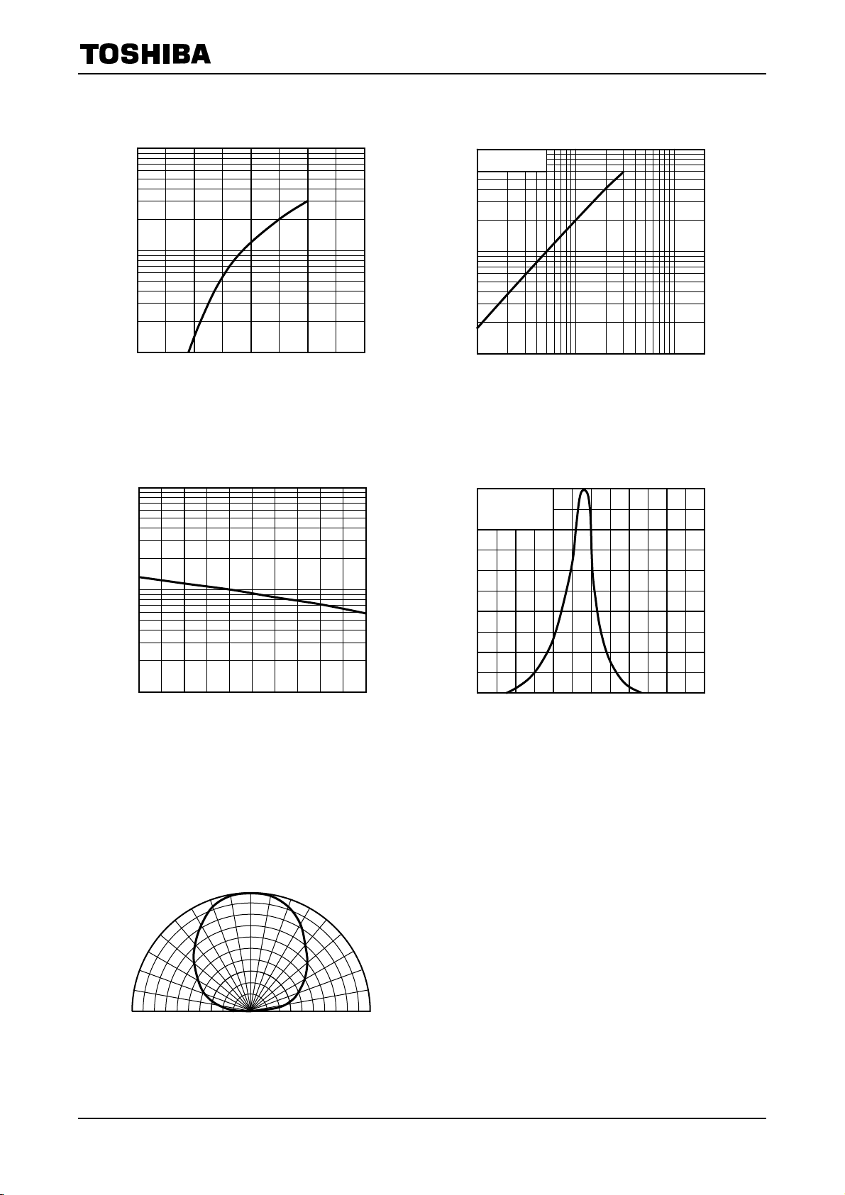
100
30
(mA)
F
10
3
Forward current I
1
1.6 1.8 2.0 2.2 2.4
Forward voltage VF (V)
I
F
– VF
1000
Ta = 25°C
500
300
(mcd)
V
100
50
30
Luminous intensity I
10
1 50
3 5 10 30 100
Forward current IF (mA)
I
V
– IF
10
V
5
3
1
0.5
0.3
Relative luminous intensity I
0.1
−25 50
0 100
Case temperature Tc (°C)
I
– Tc
V
25 75
Wavelength characteristic
1.0
IF = 20 mA
Ta = 25°C
0.8
0.6
0.4
0.2
Relative luminous intensity
0
580 620 640 660 700
600 680
Wavelength λ (nm)
Radiation pattern
Ta = 25°C
60°
70°
80°
90°
30°
40°
50°
20°
10°
10°
20°
30°
40°
50°
60°
1.00.80.6 0.4 0.2 0
70°
80°
90°
0°
4
2008-04-14
TLRMK1100C
(typ.)
(typ.)
(typ.)
(typ.)
(typ.)
TL(RK,RMK,SK,OK,YK)1100C(T11)
100
30
(mA)
F
10
3
Forward current I
1
1.6 1.8 2.0 2.2 2.4
Forward voltage VF (V)
I
F
– VF
1000
Ta = 25°C
500
300
(mcd)
V
100
50
30
Luminous intensity I
10
1 50
3 5 10 30 100
Forward current IF (mA)
I
V
– IF
10
V
5
3
1
0.5
0.3
Relative luminous intensity I
0.1
−25 50
0 100
Case temperature Tc (°C)
I
– Tc
V
25 75
1.0
IF = 20 mA
Ta = 25°C
0.8
0.6
Wavelength characteristic
0.4
0.2
Relative luminous intensity
0
580 620 640 660 700
600 680
Wavelength λ (nm)
Radiation pattern
Ta = 25°C
50°
60°
70°
80°
90°
40°
30°
20°
10°
0°
10°
20°
30°
40°
50°
60°
1.00.80.6 0.4 0.2 0
70°
80°
90°
5
2008-04-14

TLSK1100C
(typ.)
(typ.)
(typ.)
(typ.)
(typ.)
TL(RK,RMK,SK,OK,YK)1100C(T11)
100
30
(mA)
F
10
3
Forward current I
1
1.6 1.8 2.0 2.2 2.4
Forward voltage VF (V)
I
F
– VF
1000
Ta = 25°C
500
300
(mcd)
V
100
50
30
Luminous intensity I
10
1 50
3 5 10 30 100
Forward current IF (mA)
I
V
– IF
10
V
5
3
1
0.5
0.3
Relative luminous intensity I
0.1
−25 50
0 100
Case temperature Tc (°C)
I
– Tc
V
25 75
1.0
IF = 20 mA
Ta = 25°C
0.8
0.6
Wavelength characteristic
0.4
0.2
Relative luminous intensity
0
560 600 620 640 680
580 660
Wavelength λ (nm)
Radiation pattern
Ta = 25°C
40°
30°
20°
50°
60°
70°
80°
10°
0°
10°
20°
30°
40°
50°
60°
1.00.80.6 0.4 0.2 0
70°
80°
90° 90°
6
2008-04-14
TLOK1100C
(typ.)
(typ.)
(typ.)
(typ.)
(typ.)
TL(RK,RMK,SK,OK,YK)1100C(T11)
100
30
(mA)
F
10
3
Forward current I
1
1.6 1.8 2.0 2.2 2.4
Forward voltage VF (V)
I
F
– VF
1000
Ta = 25°C
500
300
(mcd)
V
100
50
30
Luminous intensity I
10
1 50
3 5 10 30 100
Forward current IF (mA)
I
V
– IF
10
V
5
3
1
0.5
0.3
Relative luminous intensity I
0.1
−25 50
0 100
Case temperature Tc (°C)
I
– Tc
V
25 75
1.0
IF = 20 mA
Ta = 25°C
0.8
0.6
Wavelength characteristic
0.4
0.2
Relative luminous intensity
0
540 580 600 620 660
560 640
Wavelength λ (nm)
Radiation pattern
Ta = 25°C
50°
60°
70°
80°
40°
30°
20°
10°
0°
10°
20°
30°
40°
50°
60°
1.00.80.6 0.4 0.2 0
70°
80°
90
° 90°
7
2008-04-14

TLYK1100C
(typ.)
(typ.)
(typ.)
(typ.)
(typ.)
TL(RK,RMK,SK,OK,YK)1100C(T11)
100
30
(mA)
F
10
3
Forward current I
1
1.6 1.8 2.0 2.2 2.4
Forward voltage VF (V)
I
F
– VF
1000
Ta = 25°C
500
300
(mcd)
V
100
50
30
Luminous intensity I
10
1 50
3 5 10 30 100
Forward current IF (mA)
I
V
– IF
10
V
5
3
1
0.5
0.3
Relative luminous intensity I
0.1
−25 50
0 100
Case temperature Tc (°C)
I
– Tc
V
25 75
1.0
IF = 20 mA
Ta = 25°C
0.8
0.6
Wavelength characteristic
0.4
0.2
Relative luminous intensity
0
540 580 600 620 660
560 640
Wavelength λ (nm)
Radiation pattern
Ta = 25°C
40°
30°
20°
50°
60°
70°
80°
90°
10°
0°
10°
20°
30°
40°
50°
60°
1.00.80.6 0.4 0.2 0
70°
80°
90°
8
2008-04-14
TL(RK,RMK,SK,OK,YK)1100C(T11)
Packaging
These LED devices are packed in an aluminum envelope with a silica gel and a moisture indicator to avoid
moisture absorption. The optical characteristics of the devices may be affected by exposure to moisture in the air
before soldering and they should therefore be stored under the following conditions:
1. This moisture proof bag may be stored unopened within 12 months at the following conditions.
Temperature: 5°C to 30°C
Humidity: 90% (max)
2. After opening the moisture proof bag, the devices should be assembled within 168 hours in an environment of
5°C to 30°C/60% RH or below.
3. If upon opening, the moisture indicator card shows humidity 30% or above (Color of indication changes to
pink) or the expiration date has passed, the devices should be baked in taping with reel.
After baking, use the baked devices within 72 hours, but perform baking only once.
Baking conditions: 60±5°C, for 12 to 24 hours.
Expiration date: 12 months from sealing date, which is imprinted on the same side as this label affixed.
4. Repeated baking can cause the peeling strength of the taping to change, then leads to trouble in mounting.
Furthermore, prevent the devices from being destructed against static electricity for baking of it.
5. If the packing material of laminate would be broken, the hermeticity would deteriorate. Therefore, do not
throw or drop the packed devices.
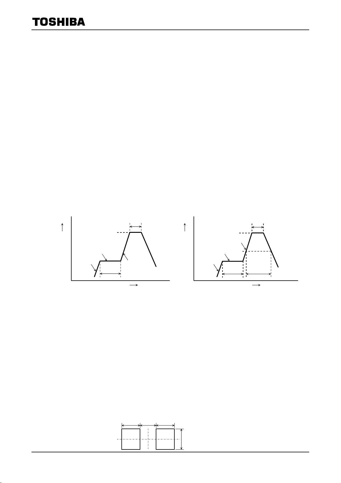
Mounting Method
Soldering
• Reflow soldering (example)
Temperature profile for Pb soldering (example)
240°C max
10 s max
(*)
(*)
Package surface
temperature (°C)
140 to 160°C
(*)
4°C/s max
60 to 120 s
max(*)
4°C/s max
max(*)
(*)
Time (s)
• The products are evaluated using above reflow soldering conditions. No additional test is performed exceed the
condition (i.e. the condition more than (*)MAX values) as a evaluation. Please perform reflow soldering under
the above conditions.
• Please perform the first reflow soldering with reference to the above temperature profile and within 168 h of
opening the package.
• Second reflow soldering
In case of second reflow soldering should be performed within 168 h of the first reflow under the above
conditions.
Storage conditions before the second reflow soldering: 30°C, 60% RH (max)
• Make any necessary soldering corrections manually.
(only once at each soldering point)
Soldering iron: 25 W
Temperature: 300°C or less
Time: within 3 s
• If the products need to be performed by other soldering method (ex. wave soldering), please contact Toshiba
sales representative.
Recommended soldering pattern
1.65 1.15
1.65
Temperature profile for Pb-free soldering (example)
(*)
5 s max
(*)
4°C/s max
230°C
(*)
60 to 120 s
Time (s)
(*)
max(*)
30 to 50 s max(*)
150 to 180°C
4°C/s max
Package surface
temperature (°C)
Unit: mm
260°C max
max(*)
2.41
9
2008-04-14

TL(RK,RMK,SK,OK,YK)1100C(T11)
Cleaning
When cleaning is required after soldering, Toshiba recommends the following cleaning solvents.
It is confirmed that these solvents have no effect on semiconductor devices in our dipping test (under the
recommended conditions). In selecting the one for your actual usage, please perform sufficient review
on washing condition, using condition and etc.
ASAHI CLEAN AK-225AES: (made by ASAHI GLASS)
KAO CLEAN TROUGH 750H: (made by KAO)
PINE ALPHA ST-100S: (made by ARAKAWA CHEMICAL)
Precautions when Mounting
Do not apply force to the plastic part of the LED under high-temperature conditions.
To avoid damaging the LED plastic, do not apply friction using a hard material.
When installing the PCB in a product, ensure that the device does not come into contact with other cmponents.
Tape Specifications
1. Product number format
The type of package used for shipment is denoted by a symbol suffix after the product number. The
method of classification is as below. (this method, however does not apply to products whose electrical
characteristics differ from standard Toshiba specifications)
(1) Tape Type: T11 (4-mm pitch)
(2) Example
TLYK1100C (T11)
2. Tape dimensions
Unit: mm
Symbol Dimension Tolerance Symbol Dimension Tolerance
D 1.5 +0.1/−0 P2 2.0 ±0.05
E 1.75 ±0.1 W 8.0 ±0.3
P0 4.0 ±0.1 P 4.0 ±0.1
t 0.3 ±0.05 A0 2.9 ±0.1
F 3.5 ±0.05 B0 3.7 ±0.1
D1 1.5 ±0.1 K0 2.3 ±0.1
Tape type
Toshiba product No.
D
P0
K
0
P
2
E
t
F
W
B
0
Polarity
A0
P D
1
10
2008-04-14
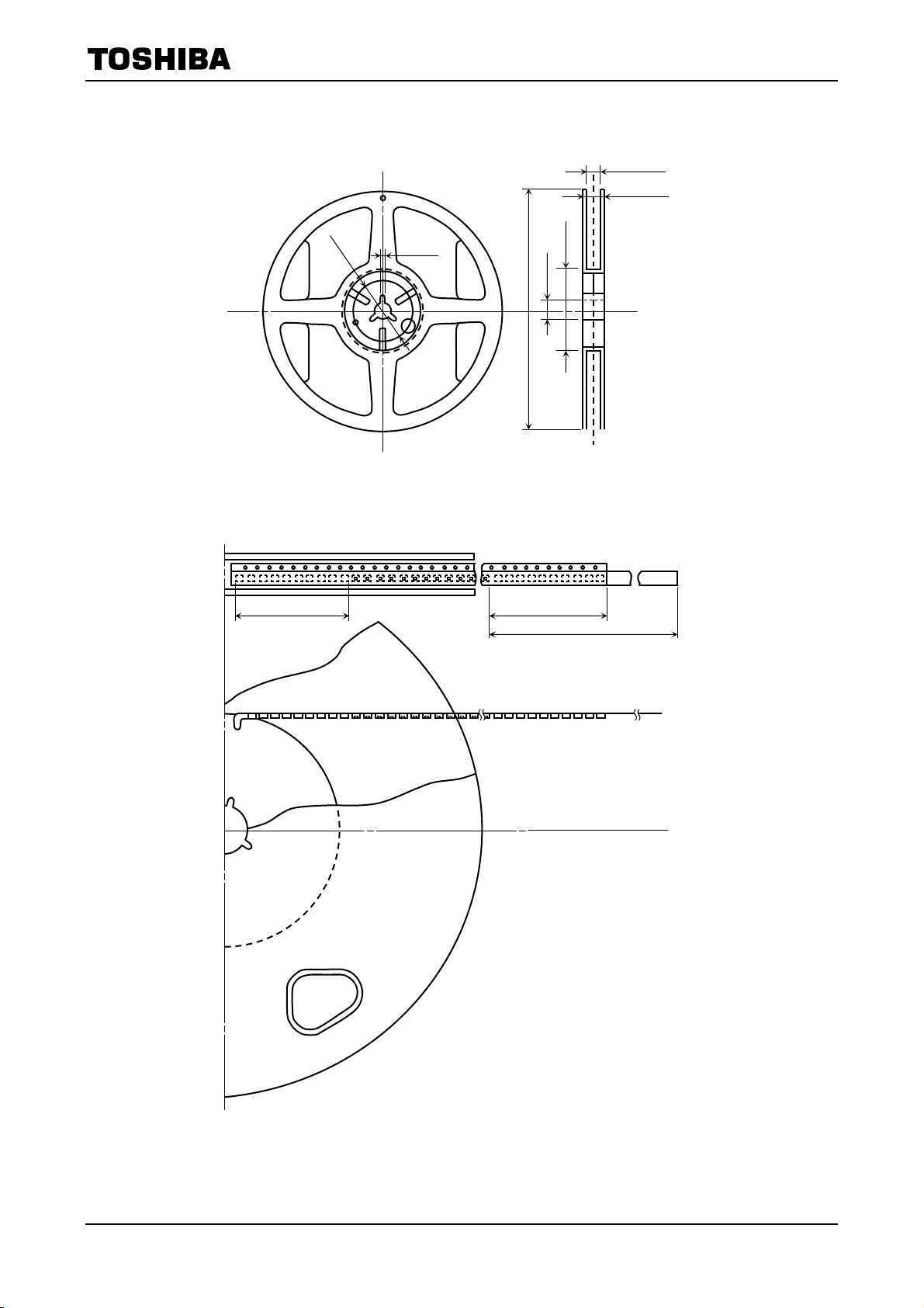
3. Reel dimensions
φ44
4. Leader and trailer sections of tape
2 ± 0.5
TL(RK,RMK,SK,OK,YK)1100C(T11)
Unit: mm
9 +1/ −0
11.4 ± 1.0
+0
−4
φ60
180
φ13
40 mm or more
(Note 1)
40 mm or more
(Note 2)
Leading part: 190 mm (min)
Note 1: Empty trailer section
Note 2: Empty leader section
11
2008-04-14

5. Packing form
•
(1) Packing quantity
(2) Packing form: Each reel is sealed in an aluminum pack with silica gel.
6. Label format
(1) Example: TLYK1100C (T11)
TL(RK,RMK,SK,OK,YK)1100C(T11)
Reel 2,000 pcs
Carton 10,000 pcs
P/N: TOSHIBA
TYPE TLYK1100C
ADDC (T11) Q’TY 2,000 pcs
Lot Number Key code for TSB 32C 2000
(RANK SYMBOL)
Use under 5-30degC/60%RH within 168h
SEALED
[[G]]/RoHS COMPATIBLE DIFFUSED IN *****
*Y380xxxxxxxxxxxxxxxxxx* ASSEMBLED IN *****
(2) Label location
• Reel
Tape feel direction
Label position
• The aluminum package in which the reel is supplied also has the label attached to
center of one side.
Carton
Label position
12
2008-04-14

TL(RK,RMK,SK,OK,YK)1100C(T11)
RESTRICTIONS ON PRODUCT USE
• The information contained herein is subject to change without notice.
• TOSHIBA is continually working to improve the quality and reliability of its products. Nevertheless, semiconductor
devices in general can malfunction or fail due to their inherent electrical sensitivity and vulnerability to physical
stress. It is the responsibility of the buyer, when utilizing TOSHIBA products, to comply with the standards of
safety in making a safe design for the entire system, and to avoid situations in which a malfunction or failure of
such TOSHIBA products could cause loss of human life, bodily injury or damage to property.
In developing your designs, please ensure that TOSHIBA products are used within specified operating ranges as
set forth in the most recent TOSHIBA products specifications. Also, please keep in mind the precautions and
conditions set forth in the “Handling Guide for Semiconductor Devices,” or “TOSHIBA Semiconductor Reliability
Handbook” etc.
• The TOSHIBA products listed in this document are intended for usage in general electronics applications
(computer, personal equipment, office equipment, measuring equipment, industrial robotics, domestic appliances,
etc.).These TOSHIBA products are neither intended nor warranted for usage in equipment that requires
extraordinarily high quality and/or reliability or a malfunction or failure of which may cause loss of human life or
bodily injury (“Unintended Usage”). Unintended Usage include atomic energy control instruments, airplane or
spaceship instruments, transportation instruments, traffic signal instruments, combustion control instruments,
medical instruments, all types of safety devices, etc.. Unintended Usage of TOSHIBA products listed in his
document shall be made at the customer’s own risk.
• The products described in this document shall not be used or embedded to any downstream products of which
manufacture, use and/or sale are prohibited under any applicable laws and regulations.
• GaAs(Gallium Arsenide) is used in this product. The dust or vapor is harmful to the human body. Do not break,
cut, crush or dissolve chemically.
20070701-EN GENERAL
• Please contact your sales representative for product-by-product details in this document regarding RoHS
compatibility. Please use these products in this document in compliance with all applicable laws and regulations
that regulate the inclusion or use of controlled substances. Toshiba assumes no liability for damage or losses
occurring as a result of noncompliance with applicable laws and regulations.
13
2008-04-14
 Loading...