


查询TLGE19TPF供应商
TLPGE19TP(F),TLFGE19TP(F),TLGE19TP(F),TLPYE19TP(F)
TOSHIBA InGaAℓP LED
TLPGE19TP(F),TLFGE19TP(F),TLGE19TP(F),TLPYE19TP(F)
Panel Circuit Indicator
• Lead(Pb)-free products (lead: Sn-Ag-Cu)
• 5mm package
• InGaAℓP technology
• All plastic mold type
• Transparent lens
• Lineup: 3colors (pure green, green, pure yellow)
• High intensity light emission
• Excellent low current light output
• Applications: Traffic signals, Safety equipment, Backlight
• Stopper lead type is also available
TLPGE19T(F), TLFGE19T(F), TLGE19T(F), TLPYE19T(F)
Lineup
Product Name Color Material
TLPGE19TP(F) Pure Green
TLFGE19TP(F) Green
TLGE19TP(F) Green
TLPYE19TP(F) Pure Yellow
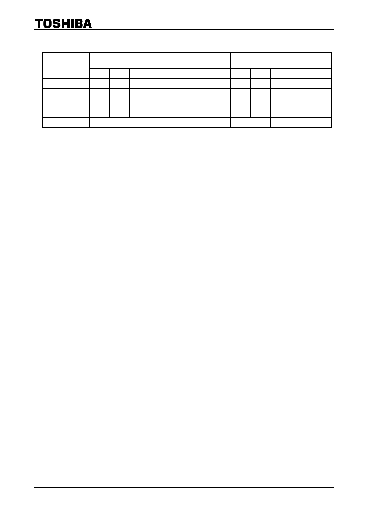
Absolute Maximum Ratings
(Ta = 25°C)
PInGaAl
Unit: mm
JEDEC ―
JEITA ―
TOSHIBA 4-5AM2
Weight: 0.31 g(Typ.)
Product Name
TLPGE19TP(F) 50 4 120
TLFGE19TP(F) 50 4 120
TLGE19TP(F) 50 4 120
TLPYE19TP(F) 50 4 120
Note: Using continuously under heavy loads (e.g. the application of high temperature/current/voltage and the
significant change in temperature, etc.) may cause this product to decrease in the reliability significantly even
if the operating conditions (i.e. operating temperature/current/voltage, etc.) are within the absolute maximum
ratings.
Please design the appropriate reliability upon reviewing the Toshiba Semiconductor Reliability Handbook
(“Handling Precautions”/“Derating Concept and Methods”) and individual reliability data (i.e. reliability test
report and estimated failure rate, etc).
Forward Current
I
(mA)
F
Reverse Voltage
VR (V)
Power Dissipation
PD (mW)
Operating
Temperature
T
(°C)
opr
−40~100 −40~120
Temperature
Storage
T
(°C)
stg
1
2007-10-01
TLPGE19TP(F),TLFGE19TP(F),TLGE19TP(F),TLPYE19TP(F)
Electrical and Optical Characteristics
(Ta = 25°C)
Product Name
TLPGE19TP(F) 558 (562) 14 20 153 500 20 2.1 2.4 20 50 4
TLFGE19TP(F) 565 (568) 15 20 272 800 20 2.0 2.4 20 50 4
TLGE19TP(F) 571 (574) 17 20 476 1300 20 2.0 2.4 20 50 4
TLPYE19TP(F) 580 (583) 14 20 476 2000 20 2.0 2.4 20 50 4
Unit nm mA mcd mA V mA μA V
Typ. Emission Wavelength
λ
λP Δλ IF Min Typ. IF Typ. Max IF Max VR
d
Luminous Intensity
I
V
Forward Voltage
VF
Reverse Current
IR
Precautions
Please be careful of the following:
• Soldering temperature: 260°C max, soldering time: 3 s max
(soldering portion of lead: up to 1.6 mm from the body of the device)
• If the lead is formed, the lead should be formed up to 1.6 mm from the body of the device without forming stress
to the resin. Soldering should be performed after lead forming.
• This visible LED lamp also emits some IR light.
If a photodetector is located near the LED lamp, please ensure that it will not be affected by this IR light.
2
2007-10-01

TLPGE19TP(F)
TLPGE19TP(F),TLFGE19TP(F),TLGE19TP(F),TLPYE19TP(F)
100
(mA)
F
Ta = 25°C
50
30
10
I
F
– VF
I
– IF
5000
Ta = 25°C
1000
(mcd)
V
V
5
3
Forward current I
1
1.7 2.1
1.8 1.9 2.2
2.0 1.6
Forward voltage VF (V)
2.3
100
Luminous intensity I
10
3 5 30 50
101
Forward current IF (mA)
100
I
– Tc
10
V
5
3
V
Relative luminous intensity – Wavelength
1.0
0.8
IF = 20 mA
Ta = 25°C
0.6
1
0.5
0.3
Relative luminous intensity I
0.1
20 −20
0 40 60
80
Case temperature Tc (°C)
0.4
0.2
Relative luminous intensity
0
560520
540 580 600 620
Wavelength λ (nm)
640
Radiation pattern
Ta
= 25°C
0°
10°
20°
60°
70°
80°
90°
30°
40°
50°
10°
20°
30°
40°
50°
60°
70°
1.00.80.6 0.4 0.2 0
80°
90°
I
– Ta
80
(mA)
F
60
40
20
F
Allowable forward current I
0
400
20 60 80 100
120
Ambient temperature Ta (°C)
3
2007-10-01

TLFGE19TP(F)
TLPGE19TP(F),TLFGE19TP(F),TLGE19TP(F),TLPYE19TP(F)
100
Ta = 25°C
50
30
(mA)
F
10
5
3
I
F
– VF
Forward current I
1
1.7 2.1
1.8 1.9 2.2
Forward voltage VF (V)
2.0 1.6
2.3
5000
1000
(mcd)
V
100
Luminous intensity I
10
I
– IF
V
Ta = 25°C
3 5 30 50
101
Forward current IF (mA)
100
10
V
5
3
I
– Tc
V
1
0.5
0.3
Relative luminous intensity I
0.1
20 −20
0 40 60
80
Case temperature Tc (°C)
1.0
0.8
0.6
0.4
0.2
Relative luminous intensity
0
Relative luminous intensity – Wavelength
IF = 20 mA
Ta = 25°C
560520
540 580 600 620
Wavelength λ (nm)
640
Radiation pattern
Ta
= 25°C
0°
10°
20°
60°
70°
80°
90°
30°
40°
50°
10°
20°
30°
40°
50°
60°
70°
1.00.80.6 0.4 0.2 0
80°
90°
4
I
– Ta
80
(mA)
F
60
40
20
F
Allowable forward current I
0
400
20 60 80 100
120
Ambient temperature Ta (°C)
2007-10-01

TLGE19TP(F)
TLPGE19TP(F),TLFGE19TP(F),TLGE19TP(F),TLPYE19TP(F)
100
Ta = 25°C
50
30
(mA)
F
10
5
3
I
F
– VF
Forward current I
1
1.7 2.1
1.8 1.9 2.2
Forward voltage VF (V)
2.0 1.6
2.3
5000
1000
(mcd)
V
100
Luminous intensity I
10
I
– IF
V
Ta = 25°C
3 5 30 50
101
Forward current IF (mA)
100
10
V
5
3
I
– Tc
V
Relative luminous intensity – Wavelength
1.0
0.8
IF = 20 mA
Ta = 25°C
0.6
1
0.5
0.3
Relative luminous intensity I
0.1
Case temperature Tc (°C)
20 −20
0 40 60
80
0.4
0.2
Relative luminous intensity
0
560520
540 580 600 620
Wavelength λ (nm)
640
Radiation pattern
20°
30°
40°
50°
60°
70°
80°
90°
10°
Ta = 25°C
0°
10°
20°
30°
40°
50°
60°
1.00.80.6 0.4 0.2 0
70°
80°
90°
I
– Ta
F
80
(mA)
F
60
40
20
Allowable forward current I
0
400
20 60 80 100
120
Ambient temperature Ta (°C)
5
2007-10-01

TLPYE19TP(F)
TLPGE19TP(F),TLFGE19TP(F),TLGE19TP(F),TLPYE19TP(F)
100
(mA)
F
Ta = 25°C
50
30
10
I
F
– VF
(mcd)
V
10000
3000
1000
Ta = 25°C
I
V
– IF
5
3
Forward current I
1
1.7 2.1
1.8 1.9 2.2
2.0 1.6
2.3
Forward voltage VF (V)
300
Luminous intensity I
100
50
330
101
100
Forward current IF (mA)
I
– Tc
10
V
5
3
V
Relative luminous intensity – Wavelength
1.0
0.8
IF = 20 mA
Ta = 25°C
0.6
1
0.5
0.3
Relative luminous intensity I
0.1
20 −20
0 40 60
80
Case temperature Tc (°C)
0.4
0.2
Relative luminous intensity
0
580540
560 600 620 640
Wavelength λ (nm)
660
80°
90°
70°
60°
50°
40°
30°
Radiation pattern
0°
20°
10°
10°
20°
Ta
= 25°C
30°
40°
50°
60°
1.00.80.6 0.4 0.2 0
70°
80°
90°
I
– Ta
80
(mA)
F
60
40
20
F
Allowable forward current I
0
400
20 60 80 100
120
Ambient temperature Ta (°C)
6
2007-10-01

TLPGE19TP(F),TLFGE19TP(F),TLGE19TP(F),TLPYE19TP(F)
RESTRICTIONS ON PRODUCT USE
• The information contained herein is subject to change without notice.
• TOSHIBA is continually working to improve the quality and reliability of its products. Nevertheless, semiconductor
devices in general can malfunction or fail due to their inherent electrical sensitivity and vulnerability to physical
stress. It is the responsibility of the buyer, when utilizing TOSHIBA products, to comply with the standards of
safety in making a safe design for the entire system, and to avoid situations in which a malfunction or failure of
such TOSHIBA products could cause loss of human life, bodily injury or damage to property.
In developing your designs, please ensure that TOSHIBA products are used within specified operating ranges as
set forth in the most recent TOSHIBA products specifications. Also, please keep in mind the precautions and
conditions set forth in the “Handling Guide for Semiconductor Devices,” or “TOSHIBA Semiconductor Reliability
Handbook” etc.
• The TOSHIBA products listed in this document are intended for usage in general electronics applications
(computer, personal equipment, office equipment, measuring equipment, industrial robotics, domestic appliances,
etc.).These TOSHIBA products are neither intended nor warranted for usage in equipment that requires
extraordinarily high quality and/or reliability or a malfunction or failure of which may cause loss of human life or
bodily injury (“Unintended Usage”). Unintended Usage include atomic energy control instruments, airplane or
spaceship instruments, transportation instruments, traffic signal instruments, combustion control instruments,
medical instruments, all types of safety devices, etc.. Unintended Usage of TOSHIBA products listed in his
document shall be made at the customer’s own risk.
• The products described in this document shall not be used or embedded to any downstream products of which
manufacture, use and/or sale are prohibited under any applicable laws and regulations.
• The information contained herein is presented only as a guide for the applications of our products. No
responsibility is assumed by TOSHIBA for any infringements of patents or other rights of the third parties which
may result from its use. No license is granted by implication or otherwise under any patents or other rights of
TOSHIBA or the third parties.
20070701-EN
• GaAs(Gallium Arsenide) is used in this product. The dust or vapor is harmful to the human body. Do not break,
cut, crush or dissolve chemically.
• Please contact your sales representative for product-by-product details in this document regarding RoHS
compatibility. Please use these products in this document in compliance with all applicable laws and regulations
that regulate the inclusion or use of controlled substances. Toshiba assumes no liability for damage or losses
occurring as a result of noncompliance with applicable laws and regulations.
7
2007-10-01
 Loading...